AMAZON multi-meters discounts AMAZON oscilloscope discounts
1. History
In the past, electrostatic discharge (ESD) testing was performed on semiconductor components. As stated in the last section, today, there is more interest in the testing of components in powered states and in electrical systems. System manufacturers have begun requiring system level testing to be done on semiconductor components, prior to final assembly and product acceptance. These system level tests are performed with an ESD gun, and without direct contact; these air discharge events produce an ESD event as well as generate EMI. In a true system, the system itself provides shielding from EMI emissions. Hence, an ESD test is of interest that has the following characteristics [1-3]:
• An IEC 61000-4-2 current waveform [4].
• No air discharge (contact discharge).
• Semiconductor component is powered during ESD testing.
• Only addresses pins and ports exposed to the external system.
The human metal model (HMM) addresses these characteristics [1-3]. This standard was released in the time frame of 2008 and 2009 [1-3]. Research in the HMM(and IEC 61000-4-2) began in the 1980s continued to recent times [1-24]. The HMM event is a recent ESD model that has increasing interest as a result of cell phone and small components with exposed ports, where field failures were evident. The HMM uses an "IEC-like" pulse waveform. The discharge from the source and the device under test (DUT) is a direct contact to avoid EMI spurious signals. The test is performed when the system is powered, and only the external ports that are exposed to the outside world are of interest.
FIG. 1 shows the cases for the HMM event. The HMM event is a direct contact event, which can be applied by an ESD gun source or a pulse source.
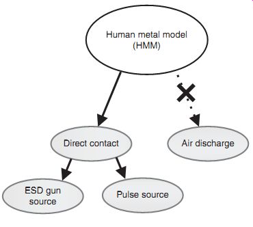
FIG. 1 Human metal model (HMM) testing overview
2. Scope
The scope of the HMMESD test is for the testing, evaluation, and classification of components to system-like ESD events. The test is to quantify the sensitivity or susceptibility of these components to damage or degradation to the defined IEC 61000-4-2 test [1-4].
3. Purpose
The purpose of the HMM ESD test is for establishment of a test methodology to evaluate the repeatability and reproducibility of systems to a defined pulse event in order to classify or compare ESD sensitivity levels of components [1-3].
4. Pulse Waveform
FIG. 2 shows an example of the HMM waveform. Note that this waveform is identical to the IEC 61000-4-2 waveform. A key difference is the HMM test only addresses direct contact discharge. The event consists of a fast high current event followed by a second slower event.
The fast event has a rise time of 0.7 to 1 ns. The slower event has a lower current with a peak at 30 ns and a decay time of 60 ns. The energy accumulation capacity is associated with a 150 pF capacitor. The discharge resistance is a 330 O resistor. This provides an 8 kV event for direct contact resistance and 15 kV event for air discharge. The polarity of the pulse event addresses positive and negative events [1-3].
4.1 Pulse Waveform Equation
For the IEC 61000-4-2 pulse waveform, an analytical formulation was established by Heidler [25, 26]. The Heidler formulation can be expressed as two exponential terms as follows:
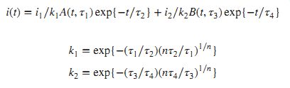
where
k1 = exp{-(?1/?2)(n?2/?1) 1/n
k2 = exp{-(?3/?4)(n?4/?3) 1/n
and additionally, A(t,?1)=(t/?1)/{1 +(t/?1) n
and B(t,?3)=(t/?3)/{1 +(t/?3) n
In this formulation, the variables i1, and i2 are currents in amperes, ?1, ?2, ?3, and ?4 are time constants in nanoseconds, and n is a constant [25, 26]. An example of parameters, for a 2 kV positive pulse, i1 =3.6A, and i2 =3.74A, ?1 =0.29, ?2 =18.44, ?3 =34.34, and ?4 =31.02 (in nanoseconds), and n=3.26 [25, 26].
5. Equivalent Circuit
FIG. 3 shows the equivalent circuit schematic for an ESD gun. The circuit schematic shows a 150 pF capacitor and a 330O resistor. The charging resistance is a 50-100 MO source. This provides an 8 kV event for direct contact resistance and 15 kV event for air discharge. The polarity of the pulse event addresses both positive and negative events.
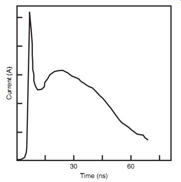
FIG. 2 Human metal model (HMM) pulse waveform
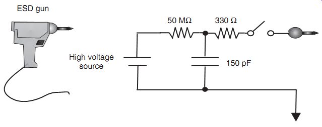
FIG. 3 Human metal model (HMM) ESD gun equivalent circuit
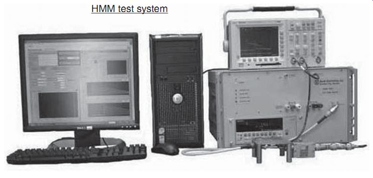
FIG. 4
Commercial HMM test system--Barth 4702 HMM+ (Barth Electronics Inc.)
6. Test Equipment
Commercial test systems now exist for device level testing to produce a waveform as specified in the IEC 61000-4-2 standard. FIG. 4 shows a photograph of the Barth Model 4702 HMM+™ test system [27]. The system was designed to eliminate the common testing issues with IEC gun testing. ESD gun testing has reproducibility and repeatability issues due to the ground cable and electromagnetic noise issues.
The Barth Model 4702 HMM tester is connected to the DUT with a single 50 Ohm coaxial cable; this cable delivers the IEC-HMM pulse and provides connection for leakage measurements between IEC stress pulse events.
The specifications for the waveform are a pulse rise time of 0.7-1.0 ns. The peak current is 3.75A/kV, a 30 ns current at 2.0A/kV, and a 60 ns current at 1.0A/kV [27]. The voltage range is from 500V to 27 kV, with a maximum current of 100A.
7. Test Configuration
The HMM testing requirements are for two different configurations. The primary reason for the specified orientation is associated with the electromagnetic field and capacitance. These will be shown in the following sections.
7.1 Horizontal Configuration
FIG. 5(a) shows the test system for a horizontal configuration. The method applies an IEC pulse to the DUT without any air discharge. Shown in the figure is an ESD gun. Measurements of 0.5m× 0.5m are required for the horizontal surface. Ground clamps are specified as well as the discharge points for application of the HMM pulse. Using a current source, variations in the ESD gun waveform and pulse variation can be removed [1-3].
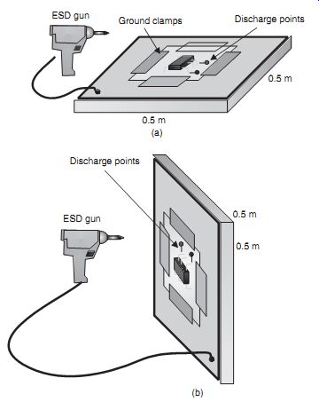
FIG. 5 (a) Human metal model (HMM)--horizontal test configuration. (b)
Human metal model (HMM) test equipment--vertical table test configuration
7.2 Vertical Configuration
FIG. 5(b) shows the test system for a vertical configuration. The method applies an IEC pulse to the DUT without any air discharge. Shown in the figure is an ESD gun. Measurements of 0.5m× 0.5mboard are required for the vertical surface. Ground clamps are specified as well as the discharge points for application of the HMM pulse. Using a current source, variations in the ESD gun waveform and pulse variation can be removed [1-3].
7.3 HMM Fixture Board
For the HMM test, test fixture boards can be integrated into the test method. FIG. 6 is an example of a schematic layout of a 50O coaxial source test fixture board. The system consists of a 50O IEC pulse source whose output is connected to the component under test.
The component under test has a bypass capacitor, an isolation inductor, and a DC power supply connected to a 54 dB attenuator. A 50O coaxial cable is also connected from the pulse source to the 54 dB attenuator. The output of the attenuator is connected to a 50 Ohm oscilloscope [1-3].
For the HMM test, the layout of the circuit board is shown in FIG. 7 [1-3]. In the test, the ground locations are specified as well as the discharge points. The definitions include the following [1-3]:
• Board ground plane
• Ground trace on the board
• Ground trace in the component
• Ground pin on socket
• Discharge point--direct to ground plane
• Discharge point--through the device
• Discharge point--to the pin to be stressed.
For the HMM test, the test can be performed with a powered board. FIG. 8 is an example of an HMM test configuration with a powered board. FIG. 8 illustrates a pulse source, a component under test, and a power source. A bypass capacitor is also placed in parallel with the component under test.
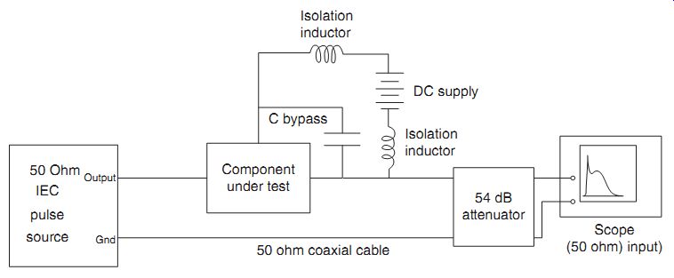
FIG. 6 Schematic layout of IEC 50O coaxial source test fixture board
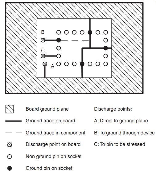
FIG. 7 Layout of IEC 50O coaxial source test fixture board showing ground
connections
FIG. 8(b) shows an example of a test fixture board for the HMM test from the Grund Technical Solutions Tarvos HMM Device Test System [40]. In the case of an ESD HMM source event, the test fixture board is used. The GTS Tarvos HMM test system applies the IEC 61000-4-2 testing pulse to packaged devices, boards, and subassemblies with the use of a 50O cable. This allows for a reproducible and repeatable pulse waveform.
8. Test Sequence and Procedure
FIG. 9 shows the HMM test sequence and procedure. The procedure is as follows [1-3]:
• Choose a test configuration.
• Wire only external ports in the test fixture.
• Mount the DUT.
• Choose the reference and the pin under test (PUT).
• Charge the HMM source to a specified test level.
• Discharge HMM source to the PUT.
• Evaluate the leakage.
• Evaluate the leakage failure criteria.
• If no failure occurs, retest to a higher current level; if failure occurs, discontinue testing of the PUT.
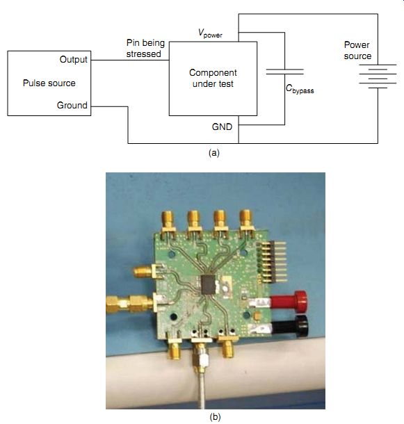
FIG. 8
(a) HMM with powered board. (b) Human metal model (HMM) source test fixture
board (Grund Technical Solutions)
8.1 Current Waveform Verification
For the testing procedure, it is important to verify the current waveform. For this to be per formed correctly, the physical arrangement for testing is critical. FIG. 10 shows an example of the physical arrangement for HMM current waveform verification [1-3].
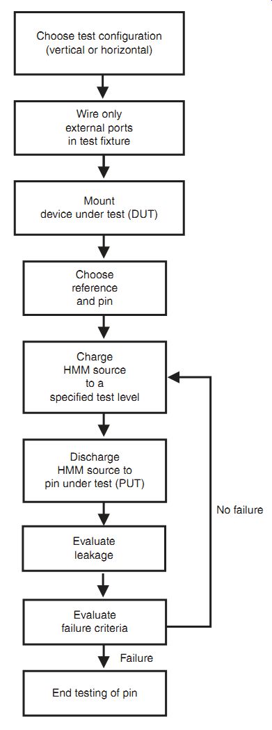
FIG. 9 Human metal model (HMM) test sequence
2. Current Probe Verification Methodology
For the current probe verification methodology, current probes must be evaluated for proper testing of the HMM event. FIG. 11 shows a procedure of simultaneous measurement of the IEC probe, and the Fischer Custom Communication current probe F65-A [28]. The two probes are actually utilized in a simultaneous fashion [1-3].
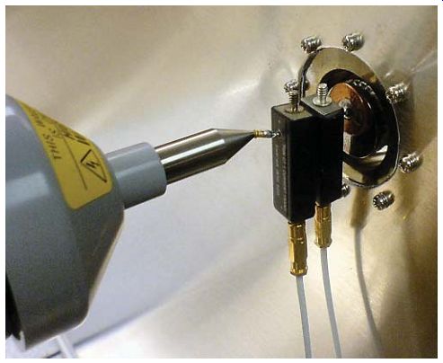
FIG. 10 Human metal model (HMM) current waveform verification--physical
arrangements.
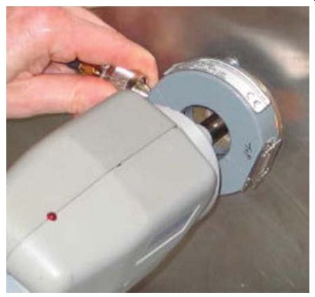
FIG. 11 Simultaneous measurement of current probe IEC and the Fischer
Custom Communication current probe F-65A.
3. Current Probe Waveform Comparison
For the current probe waveform comparison, three tests were performed:
• IEC current probe only
• IEC with F-65A current probes [28]
• F-65A with IEC current probes [28].
FIG. 12 shows a procedure of simultaneous measurement of the IEC probe and the Fischer Custom Communication current probe F65-A. The two probes are actually utilized in a simultaneous fashion.
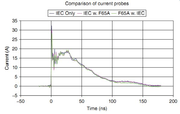
FIG. 12 Human metal model (HMM) current probe waveform comparison
9. Failure Mechanisms
The failure mechanisms for the HMM event are equivalent to the failures that occur in the IEC 61000-4-2, with a few distinctions:
• The HMM pulse is applied only to specific pins that are connected to external ports.
• The HMM pulse failures can occur on pins that are not connected to external ports.
In the case of pins connected to external ports, HMM failures can occur in the following:
• Bond pad
• Interconnects between bond pad and ESD network
• ESD network
• I/O networks
• VDD power rail
• VSS power rail.
In the case of pins not connected to external ports, HMM failures can occur through the common power rails.
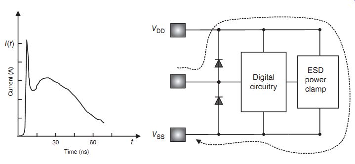
FIG. 13 HMM ESD event current paths--VSS positive polarity
10. ESD Current Paths
In the case of pins not connected to external ports, HMM failures can occur through the common power rails. FIG. 13 shows an HMM event lowing into the designated signal pin (which is an external port). The distinction in this event from a typical HBM event is that the current can be significant due to the fast high current pulse event at the onset of the event.
Second, this is only the testing of an external port signal pin. Another distinction is that the current into the VSS ground rail can impact the other internal circuitry not shown in the picture [31, 36, 38].
11. ESD Protection Circuit Solutions
FIG. 14 shows a solution to provide ESD protection to the semiconductor component [29-40]. The key issue is that a low resistance path between the external port pin and its local power connection is desired to discharge the current. The width of the interconnects must be able to survive the current magnitude of the HMM pulse event. In addition, it is desired that the current does not low into the power grid adjacent to the other non-external port pins. This is achievable by providing the following design layout features:
• A dedicated HMM VDD power pad adjacent to the external port signal pin
• A dedicated power HMM VDD interconnect power bus
• A dedicated HMM VSS power pad adjacent to the external port signal pin
• A dedicated HMM VSS interconnect power bus
• Electrical connection between the HMM VDD power bus and the VDD power bus (e.g., a resistive connection)
• Electrical connection between the HMM VSS power bus and the VSS power bus (e.g., a resistive connection).
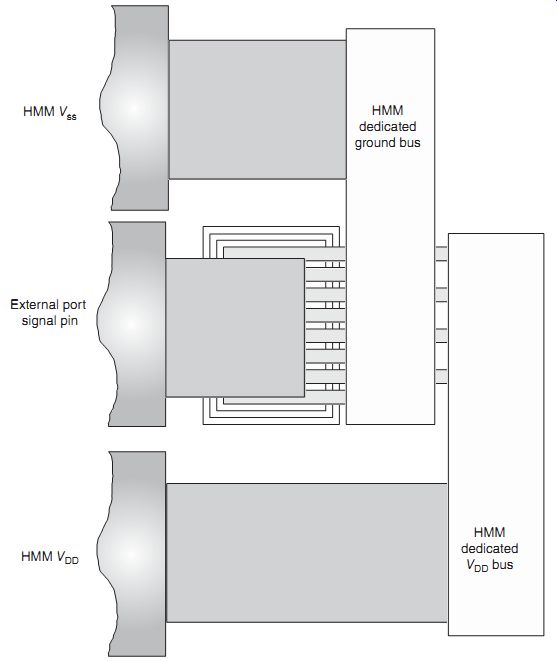
FIG. 14 Human metal model (HMM) ESD protection solution--dedicated VDD
and VSS power bus
The electrical connections are highlighted in FIG. 15. The HMM bus resistance terms are designed significantly lower to allow current to low to the respective power rails. In addition, the bus resistance to the power clamp and the resistance internal to the core are critical on how the HMM current distributes through the semiconductor component. The resistance to the power clamp local to the external port should have a low enough resistance to allow operability, but not to allow the high current peak to lead to electrical overstress (EOS) of the MOSFET gate structure.
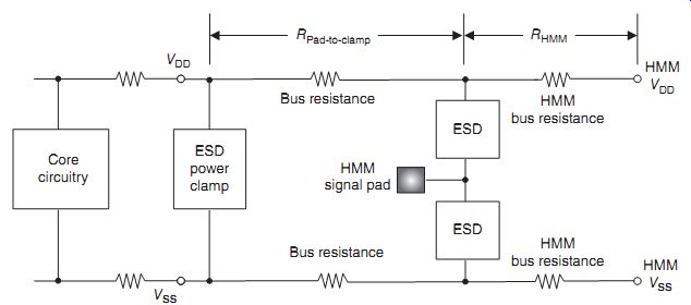
FIG. 15 Human metal model (HMM) ESD event--power grid definition
12. Summary and Closing Comments
This section addressed a new semiconductor chip level test to address IEC 61000-4-2 pulse events into external ports of a semiconductor chip. This test, the HMM, introduces a fast transient followed by a slower HBM-like waveform that is only applied to specific ports exposed on a system level. With the growing interest in system level EOS, the interest in this test has emerged recently due to the request of system level developer for the semiconductor chip suppliers.
Section 9 addresses system level transient surge concerns in semiconductor development known as IEC 61000-4-5. This test introduces a transient oscillation. With the growing interest in system level EOS, the interest in this test has emerged recently in semiconductor chip sup pliers to test equipment. The section addresses the purpose, the scope, and the pulse waveform. ESD protection concepts for the IEC 61000-4-5 are also discussed.
Problems
1. The IEC 61000-4-2 can be an air discharge event. What parameter variables influence the pulse waveform when it is an air discharge event? The HMM pulse event is a direct contact methodology. What parameter variables influence the pulse waveform of the HMM event?
2. The IEC 61000-4-2 discharge for an air discharge initiated an E- and H-field outside of the electronic system. Estimate the energy in the E-field and the H-field assuming a current pulse of current I. The HMM event is a direct contact event. Calculate the ratio of energy in the E and H field over the total energy of the system.
3. The IEC 61000-4-2 discharge for an air discharge initiated an E- and H-field outside of the electronic system. Estimate the energy in the E-field and the H-field assuming a current pulse of current I. The HMM event is a direct contact event. Calculate the ratio of energy of the HMM event over the total energy.
4. Why should we exclude the energy of the E-field and H-field for evaluation of the ESD robustness of semiconductor chips that are contained within systems?
5. An ESD gun can be used to initiate a direct HMM discharge to a cell phone that contains external port for charging of the cell phone. What factors influence the discharge event?
6. An ESD gun can be used to initiate a direct HMM discharge to a laptop. What are potential sources of system failures? Assume the discharge is to the laptop USB ports. What factors influence the discharge event?
7. An ESD gun is used to zap an antennae of a cell phone. The cell phone is electrically connected to a gallium arsenide (GaAs) bipolar transistor power amplifier. Show the ESD event. What ESD protection circuitry can be used to avoid failure of the GaAs cell phone power amplifier?
References
[not listed]