AMAZON multi-meters discounts AMAZON oscilloscope discounts
Crosstalk, which is the coupling of energy from one line to another, will occur whenever the electromagnetic fields from different structures interact. In digital designs the occurrence of crosstalk is very widespread. Crosstalk will occur on the chip, on the PCB board, on the connectors, on the chip package, and on the connector cables. Furthermore, as technology and consumer demands push for physically smaller and faster products, the amount of crosstalk in digital systems is increasing dramatically. Subsequently, crosstalk will introduce significant hurdles into system design, and it’s vital that the engineer learn the mechanisms that cause crosstalk and the design methodologies to compensate for it.
In multiconductor systems, excessive line-to-line coupling, or crosstalk, can cause two detrimental effects. First, crosstalk will change the performance of the transmission lines in a bus by modifying the effective characteristic impedance and propagation velocity, which will adversely affect system-level timings and the integrity of the signal. Additionally, crosstalk will induce noise onto other lines, which may further degrade the signal integrity and reduce noise margins. These aspects of crosstalk make system performance heavily dependent on data patterns, line-to-line spacing, and switching rates. In this section we introduce the mechanisms that cause crosstalk, present modeling methodology, and elaborate on the effects that crosstalk has on system-level performance.
1. MUTUAL INDUCTANCE AND MUTUAL CAPACITANCE
Mutual inductance is one of the two mechanisms that cause crosstalk. Mutual inductance Lm induces current from a driven line onto a quiet line by means of the magnetic field.
Essentially, if the "victim" or quiet trace is in close enough proximity to the driven line such that its magnetic field encompasses the victim trace, a current will be induced on that line.
The coupling of current via the magnetic field is represented in the circuit model by a mutual inductance.
The mutual inductance Lm will inject a voltage noise onto the victim proportional to the rate of change of the current on the driver line. The magnitude of this noise is calculated as (1)
Since the induced noise is proportional to the rate of change, mutual inductance becomes very significant in high-speed digital applications.
Mutual capacitance is the other mechanism that causes crosstalk. Mutual capacitance is simply the coupling of two conductors via the electric field. The coupling due to the electric field is represented in the circuit model by a mutual capacitor. Mutual capacitance Cm will inject a current onto the victim line proportional to the rate in change of voltage on the driven line: (2)
Again, since the induced noise is proportional to the rate of change, mutual capacitance also becomes very significant in high-speed digital applications.
It should be noted that equations (1) and (2) are only simple approximations used to explain the mechanisms of the coupled noise. Complete crosstalk formulas are presented later in the Section.
2. INDUCTANCE AND CAPACITANCE MATRIX
In systems where significant coupling occurs between transmission lines, it’s no longer adequate to represent the electrical characteristics of the line with just an inductance and a capacitance, as could be done with the single-transmission-line case presented in Section 2.
It becomes necessary to consider the mutual capacitance and mutual inductance to fully evaluate the electrical performance of a transmission line in a multiconductor system.
Equations (3) and (4) depict the typical method of representing the parasitics that govern the electrical performance of a coupled transmission line system. The inductance and capacitance matrices are known collectively as the transmission line matrices. The example shown is for an N-conductor system and is representative of what is usually reported by a field simulator (see Sect. 3), which is a tool used to calculate the inductance and capacitance matrices of a transmission line system.
(3)
...where LNN is the self-inductance of line N and LMN is the mutual inductance between lines M and N. (4)
…where CNN is the total capacitance seen by line N, which consists of conductor N's capacitance to ground plus all the mutual capacitance to other lines and CNM = mutual capacitance between conductors N and M.
Example 1: Two-Conductor Transmission Line Matrices.
The capacitance matrix for FIG. 1 is (5) ... where the self-capacitance of line 1, C11, is the sum of the capacitance of line 1 to ground ( ) plus the mutual capacitance from line 1 to line 2 (C12): (6)
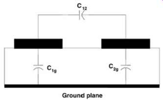
FIG. 1: Simple two-conductor system used to explain the parasitic matrices.
Additionally, the inductance matrix for the system depicted in FIG. 1
is (7) where L11 is the self-inductance for line 1 and L12 is the mutual inductance
between lines 1 and 2. L11 is not the sum of the self-inductance and the
mutual inductance as in the case of C11.
3. FIELD SIMULATORS
Field simulators are used to model the electromagnetic interaction between transmission lines in a multiconductor system and to calculate trace impedances, propagation velocity, and all self and mutual parasitics. The outputs are typically matrices that represent the effective inductance and capacitance values of the conductors. These matrices are the basis of all equivalent circuit models and are used to calculate characteristic impedance, propagation velocity, and crosstalk. Field simulators fall into two general categories: two dimensional, or electrostatic, and three-dimensional, or full-wave. Most two-dimensional simulators will give the inductance and capacitance matrices as a function of conductor length, which is usually most suitable for interconnect analysis and modeling. The advantage of the two-dimensional or electrostatic simulators is that they are very easy to use and typically take a very short amount of time to complete the calculations. The disadvantages of two-dimensional simulators are that they will simulate only relatively simple geometries, they are based on static calculations of the electric field, and they usually don’t calculate frequency-dependent effects such as internal inductance or skin effect resistance. This is usually not a significant obstacle, however, since interconnects are usually simple structures and there are alternative methods of calculating effects such as frequency-dependent resistance and inductance.
Additionally, there are several three-dimensional, or full-wave simulators on the market. The advantage of a full-wave simulator is that they will simulate complex three-dimensional geometries, and they will predict frequency-dependent losses, internal inductance, dispersion, and most other electromagnetic phenomena, including radiation. The simulators essentially solve Max-well's equations directly for an arbitrary geometry. The disadvantage is that they are very difficult to use, and simulations typically take hours or days rather than seconds. Additionally, the output from a full-wave simulator is often in the form of S parameters, which are not very useful for interconnect simulations for digital applications.
For the purposes of this guide, emphasis is placed on electrostatic two-dimensional simulators.
4. CROSSTALK-INDUCED NOISE
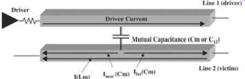
FIG. 2: Crosstalk-induced current trends caused by mutual inductance and
mutual capacitance.
As explained in Sect. 1, crosstalk is the result of mutual capacitance Cm in conjunction with mutual inductance Lm between adjacent conductors. The magnitude of the noise induced onto the adjacent transmission lines will depend on the magnitude of both the mutual inductance and the mutual capacitance. For example, if a signal is injected into line 1 of FIG. 2, current will be generated on the adjacent line by means of Lm and Cm. For simplicity, let us define a few terms. Near-end crosstalk is defined as the crosstalk seen on the victim line at the end closest to the driver (this is sometimes called backward crosstalk). Far-end crosstalk refers to the crosstalk observed on the victim line farthest away from the driver (sometimes known as forward crosstalk). The current generated on the victim line due to mutual capacitance will split and flow toward both ends of the adjacent line. The current induced onto the victim line as a result of the mutual inductance will flow from the far end toward the near end of the victim line since mutual inductance creates current flow in the opposite direction. As a result, the crosstalk currents flowing toward the near and far ends can be broken down into several components (see FIG. 2):
(8)
(9)
The shape of the crosstalk noise seen at the near and far ends of the victim line can be deduced by looking at FIG. 3. As a digital pulse travels down a transmission line, the rising and falling edges will induce noise continuously on the adjacent line. For this discussion, assume that the rise and fall times are much smaller than the delay of the line.
As described previously, a portion of the crosstalk noise will travel toward the near end of the line and a portion will travel toward the far end. The portions traveling toward the near and far ends will be referred to as the near- and far-end crosstalk pulses, respectively. As depicted by FIG. 3, the far-end crosstalk pulse will travel concurrently with the edge of the signal on the driving line. The near-end crosstalk pulse will originate at the edge and propagate back toward the near end. Subsequently, when the signal edge reaches the far end of the driving line at time t = TD (where TD is the electrical delay of the transmission line), the driving signal and the far-end crosstalk will be terminated by the resistor. The last portion of the near-end crosstalk induced on the victim line just prior to the signal being terminated, however, won’t arrive at the near end until time t = 2TD because it must propagate the entire length of the line to return. Therefore, for a pair of terminated transmission lines, the near-end crosstalk will begin at time t = 0 and have a duration of 2TD, or twice the electrical length of the line. Furthermore, the far-end crosstalk will occur at time t = TD and have a duration approximately equal to the signal rise or fall time.
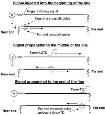
FIG. 3: Graphical representation of crosstalk noise.
The magnitude and shape of the crosstalk noise depend heavily on the amount of coupling and the termination. The equations and illustrations in FIG. 4 describe the maximum voltage levels induced on a quiet victim line as a result of crosstalk, assuming a variety of victim line termination strategies [DeFalco, 1970]. The driving line is terminated to eliminate complications due to multiple reflections. These equations should be used primarily to estimate the magnitude of crosstalk noise and to understand the impact of a particular termination strategy. For topologies more complicated then the ones shown in FIG. 4, a simulator such as SPICE is required.
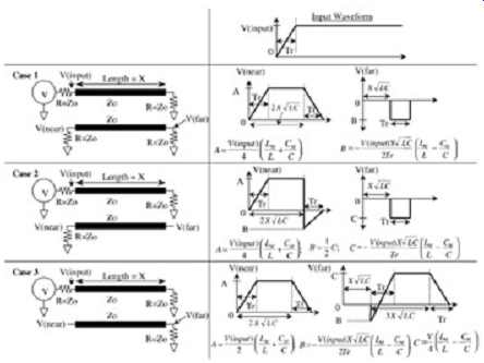
FIG. 4: Digital crosstalk noise as a function of victim termination.
The equations in FIG. 4 assume that the line delay TD is at least twice the rise time: (10) where X is the line length and L and C are the self-inductance and capacitance of the transmission line per unit length. Note that if Tr > 2X (i.e., the edge rate is greater than twice the line delay), the near-end crosstalk will fail to achieve its maximum amplitude. To calculate the correct crosstalk voltages when Tr > 2X , simply multiply the near-end crosstalk by 2X /Tr. The far-end crosstalk equations don’t need to be adjusted.
Note that the near-end crosstalk is independent of the input rise time when the rise time is short compared to the line delay (long-line case) and is dependent on the rise time when the rise time is long compared to the line length (short-line case). For this subject matter, the definition of a long line is when the electrical delay of the line is at least one-half the signal rise time (or fall time). Moreover, the near-end magnitude is independent of length for the long-line case, while the far end always depends on rise time and length.
It should be noted that the formulas in FIG. 4 assume that the termination resistors on the victim line are matched to the transmission line, which eliminates any effects of imperfect terminations. To compensate for this, simply use the transmission line reflection concepts introduced in Section 2. For example, assume that the termination R in case 1 of FIG. 4 is not equal to the characteristic impedance of the victim transmission line (for simplicity, it will still be assumed that the termination on the driver line remains perfectly matched to its characteristic impedance). In this case the near- and far-end reflections must be added to the respective crosstalk voltages. The resultant crosstalk signal, accounting for nonideal terminations, is calculated as (11) … where Vx is the crosstalk at the near or far end of the victim line adjusted for a nonperfect termination, R the impedance of the termination, Zo the characteristic impedance of the transmission line, and Vcrosstalk the value calculated from FIG. 4.
POINTS TO REMEMBER
-- If the rise or fall time is short compared to the delay of the line, the near-end crosstalk noise is independent of the rise time.
-- If the rise or fall time is long compared to the delay of the line, the near-end crosstalk noise is dependent on the rise time.
-- The-far end crosstalk is always dependent on the rise or fall time.
Example 2: Calculating Crosstalk-Induced Noise for a Matched Terminated System.
Assume the two-conductor system shown in FIG. 5, where Zo ˜ 70 ?, the termination resistors = 70 ?, V(input) = 1.0 V, Tr = 100 ps, and X = 2 in. Determine the near- and far-end crosstalk magnitudes assuming the following capacitance and inductance matrices:
FIG. 5: Near- and far-end crosstalk pulses.
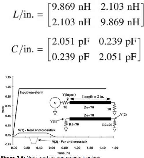
FIG. 5 also shows a simulation of the system in this example. It can readily
be seen that the near- and far-end crosstalk-induced noise matches the equations
of FIG. 4.
SOLUTION:
Example 3: Calculating Crosstalk-Induced Noise for a Non-matched Terminated System.
Consider the same two-conductor system of Example 2. If R1 = 45 and R2 = 100 ?, what are the respective near- and far-end crosstalk voltages?
SOLUTION:
5. SIMULATING CROSSTALK USING EQUIVALENT CIRCUIT MODELS
Equivalent circuit models are the most general method of simulating crosstalk. FIG. 6 depicts an N-segment equivalent circuit model of two coupled lines as modeled in SPICE, where N is the number of sections required such that the model will behave as a continuous transmission line and not as a series of lumped inductors, capacitors, and resistors. As mentioned in Section 2, the number of segments, N, in a transmission line model depends on the fastest edge rate used in the simulation. A good rule of thumb is that the propagation delay of a single segment should be less than or equal to one-tenth of the rise time (see Section 2 for a full explanation).
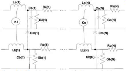
FIG. 6: Equivalent circuit model of two coupled lines. The mutual inductance
is typically modeled in SPICE-type simulators with a coupling factor K:
(12) … where L12 is the mutual inductance between lines 1 and 2, and L11
and L22 are the self inductances of lines 1 and 2, respectively.
Example 4: Creating a Coupled Transmission Line Model.
Assume that a pair of coupled transmission lines is 5 in. long and a digital signal with a rise time of 100 ps is to be simulated. Given the following inductance and capacitance matrices, calculate the characteristic impedance, the total propagation delay, the inductive coupling factor, the number of required segments, the maximum delay per segment, and the maximum L, R, C, G, Cm, and K values for one segment.
SOLUTION: Characteristic impedance:
Total propagation delay:
Inductive coupling factor:
Minimum number of segments (see Section 2):
The transmission line is 5 in. long and there need to be a minimum of 67 total segments for the model to behave like a transmission line. Subsequently, since the capacitance and inductance matrices are reported per unit inch, the L, C, and Cm values must be multiplied by (in./segment). Subsequently, L(N) = 0.67 nH, Cg(N) = C11 - C12 = 0.1425 pF, and Cm(N) = 0.0075 pF. Since the inductive coupling factor K has no units [as calculated with equation (12) all the units cancel], it’s not necessary to scale it for each segment. Therefore, K(N) = 0.078.
6. CROSSTALK-INDUCED FLIGHT TIME AND SIGNAL INTEGRITY VARIATIONS
The effective characteristic impedance and propagation delay of a transmission line will change with different switching patterns in systems where significant coupling between traces exists. Electric and magnetic fields interact in specific ways that depend on the data patterns on the coupled traces. These specific patterns can effectively reduce or increase the effective parasitic inductance and capacitance seen by a single line. Since the transmission line parameters vary with data patterns and are essential for accurate timing and signal integrity analysis, it’s important to consider these variations in high-trace-density and high-speed systems. In this section we explain the effect that crosstalk-induced impedance and velocity changes will have on signal integrity and timings. Additionally, simplified signal integrity analysis methodologies, which correctly model multiple conductors in a computer bus, will be introduced.
6.1. Effect of Switching Patterns on Transmission Line
Performance When multiple traces are in close proximity, the electric and magnetic fields will react with each other in specific ways that depend on the signal patterns present on the lines. The significance of this is that these interactions will alter the effective characteristic impedance and the velocity of the transmission lines. This phenomenon is magnified when many transmission lines are switching in close proximity to one another, and it effectively causes a bus to exhibit pattern-dependent impedance and velocity behavior. This can significantly affect the performance of a bus, so it’s imperative to consider it in system design.
Odd Mode.
Odd-mode propagation mode occurs when two coupled transmission lines are driven with equal magnitude and 180° out of phase with one another. The effective mutual capacitance of the transmission line will increase by twice the mutual capacitance, and the equivalent inductance will decrease by the mutual inductance. To examine the effect that odd-mode propagation on two adjacent traces will have on the characteristic impedance and on the velocity, consider FIG. 7.
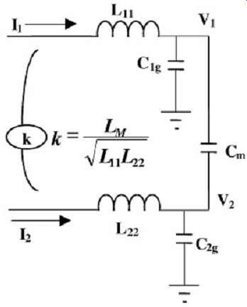
FIG. 7: Equivalent circuit model used to derive the impedance and velocity
variations for odd- and even-mode switching patterns.
In odd-mode propagation, the currents on the lines, I1 and I2, will always be driven with equal magnitude but in opposite directions. First, let's consider the effect of mutual inductance.
Refer to FIG. 8. Assume that L11 = L22 = L0. Remember that the voltage produced by the inductive coupling is calculated by equation (1). Subsequently, applying Kirchhoff's voltage law produces
(13)
(14)
FIG. 8: Simplified circuit for determining the equivalent odd-mode inductance. Since the signals for odd-mode switching are always opposite, it’s necessary to substitute I1 = -I2 and V1 = -V2 into (13) and (14). This yields
(15)
(16)
Therefore, the equivalent inductance seen by line 1 in a pair of coupled transmission lines propagating in odd mode is (17)
FIG. 9: Simplified circuit for determining the equivalent odd mode capacitance.
Similarly, the effect of the mutual capacitance can be derived. Refer to
FIG. 9. Applying Kirchhoff's current law at nodes V1 and V2 yields (assume
that )
(18)
(19)
Again, substitution of I1 = -I2 and V1 = -V2 for odd-mode propagation yields (20) (21)
Therefore, the equivalent capacitance seen by trace 1 in a pair of coupled transmission line propagating in odd mode is
(22)
Subsequently, the equivalent impedance and delay for a coupled pair of transmission lines propagating in an odd-mode pattern are
(23)
(24)
Even Mode.
Even-mode propagation mode occurs when two coupled transmission lines are driven with equal magnitude and are in phase with one another. The effective capacitance of the transmission line will decrease by the mutual capacitance and the equivalent inductance will increase by the mutual inductance. To examine the effect that even-mode propagation on two adjacent traces will have on the characteristic impedance and on the velocity, consider FIG. 7.
In even-mode propagation, the currents on the lines, I1 and I2, will always be driven with equal magnitude and in the same direction. First, let's consider the effect of mutual inductance. Again, refer to FIG. 8. The analysis that was done for odd-mode switching can be done to determine the effective even-mode capacitance and inductance. For even mode propagation, I1 = I2 and V1 = V2; therefore, equations (13) and (14) yield (25)
(26)
Therefore, the equivalent inductance seen by line 1 in a pair of coupled transmission line propagating in even mode is
(27)
Similarly, the effect of the mutual capacitance can be derived. Again, refer to FIG. 9.
Substituting I1 = I2 and V1 = V2 for even-mode propagation, therefore, equations (18) and (19) yield (28)
(29)
Therefore, the equivalent capacitance seen by trace 1 in a pair of coupled transmission line propagating in even mode is (30) Subsequently, the even-mode transmission characteristics for a coupled two-line system are (31)
(32)
FIG. 10 depicts the odd- and even-mode electric and magnetic field patterns for a simple two-conductor system. As explained in Section 2, the magnetic field lines will always be perpendicular to the electric field lines (assuming TEM mode). Notice that both conductors are at the same potential for even-mode propagation. Since there is no voltage differential, there can be no effect of capacitance between the lines. This is an easy way to remember that the mutual capacitance is subtracted from the total capacitance for the even mode.
Since the conductors are always at different potentials in odd-mode propagation, an effect of the capacitance between the two lines must exist. This is an easy way to remember that you add the mutual capacitance for odd mode.
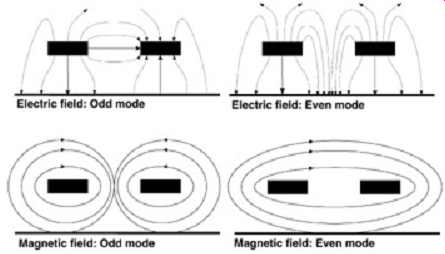
FIG. 10: Odd- and even-mode electric and magnetic field patterns for a
simple two conductor system.
FIG. 11 demonstrates how odd- and even-mode impedance and velocity changes will affect the signals propagating on a transmission line. Although there are only three conductors in this example, the simulation shows the effect that crosstalk will have on a given net, which is routed between other nets in a computer bus. The figure shows that signal integrity and velocity (assuming a microstrip) can be affected dramatically by the crosstalk and is a function of switching patterns. Since signal integrity depends directly on the source (buffer) and transmission line impedance, the degree of coupling and the switching pattern will significantly affect system performance, due to the fact that the effective characteristic impedance of the traces will change. Moreover, if the transmission line is a microstrip, the velocity will change, which will affect timings, especially for long lines.
This type of analysis using three conductors is usually adequate for design purposes and is a good first-order approximation of the true system performance because the nearest neighbor lines have the most significant effect.
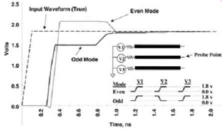
FIG. 11: Effect of switching patterns on a three-conductor system.
It’s interesting to note that the mutual inductance is always added or subtracted in the opposite manner as the mutual capacitance for odd- and even-mode propagation. This can be visualized by looking at the fields in FIG. 10. For example, in odd-mode propagation, the effect of the mutual capacitance must be added because the conductors are at different potentials. Additionally, since the currents in the two conductors are always flowing in opposite directions, the currents induced on each line due to the coupling of the magnetic fields always oppose each other and cancel out any effect due to the mutual inductance.
Subsequently, the mutual inductance must be subtracted and the mutual capacitance must be added to calculate the odd-mode characteristics.
These characteristics of even- and odd-mode propagation are due to the assumption that the signals are propagating only in TEM (transverse electro-magnetic) mode, which means that the electric and magnetic fields are always orthogonal to each other. As a result of the TEM assumption, the product of L and C remain constant for homogeneous systems (where the fields are contained within a single dielectric). Thus, in a multiconductor homogeneous system, such as a stripline array, if L is increased by the mutual inductance, C must be decreased by the mutual capacitance such that LC remains constant. Subsequently, a stripline or buried microstrip which is embedded in a homogeneous dielectric should not exhibit velocity variations due to different switching modes. It will, however, exhibit pattern dependent impedance differences.
In a non-homogeneous system (where the electric fields will fringe through more than one dielectric material) such as an array of microstrip lines, LC is not held constant for different propagation modes because the electromagnetic fields are traveling partially in air and partially in the dielectric material of the board. In a microstrip system the effective dielectric constant is a weighted average between air and the dielectric material of the board. Because the field patterns change with different propagation modes, the effective dielectric constant will change depending on the field densities contained within the board dielectric material and the air. Thus the LC product will be mode dependent in a non-homogeneous system.
The LC product will, however, remain constant for a given mode. Subsequently, a microstrip will exhibit both a velocity and impedance change, due to different switching patterns.
POINTS TO REMEMBER
-- Odd-mode impedance will always be lower than the single-line case.
-- Even-mode impedance will always be higher than the single-line case.
-- There are no velocity variations due to crosstalk in a stripline.
-- Crosstalk will induce velocity variations in a microstrip.
6.2. Simulating Traces in a Multiconductor System Using a Single-Line Equivalent Model
Two coupled conductors can be modeled as one conductor by determining the effective odd- or even-mode impedance and propagation delay of the transmission line pair and substituting these parameters into a single-line model. This technique can be expanded to determine the effective crosstalk-induced impedance and delay variations for a multiconductor system. This will allow the designer to estimate the worst-case effects of crosstalk during a bus design prior to an actual layout. This greatly increases the efficiency of the pre-layout design because it’s significantly less computationally intense than simulating with equivalent circuit models, and it allows crosstalk-induced impedance and velocity changes to be accounted for early in the design process.
It’s interesting to note that the mutual inductance is always added or subtracted in the opposite manner as the mutual capacitance for odd- and even-mode propagation. This can be visualized by looking at the fields in FIG. 10. For example, in odd-mode propagation, the effect of the mutual capacitance must be added because the conductors are at different potentials. Additionally, since the currents in the two conductors are always flowing in opposite directions, the currents induced on each line due to the coupling of the magnetic fields always oppose each other and cancel out any effect due to the mutual inductance.
Subsequently, the mutual inductance must be subtracted and the mutual capacitance must be added to calculate the odd-mode characteristics.
These characteristics of even- and odd-mode propagation are due to the assumption that the signals are propagating only in TEM (transverse electro-magnetic) mode, which means that the electric and magnetic fields are always orthogonal to each other. As a result of the TEM assumption, the product of L and C remain constant for homogeneous systems (where the fields are contained within a single dielectric). Thus, in a multiconductor homogeneous system, such as a stripline array, if L is increased by the mutual inductance, C must be decreased by the mutual capacitance such that LC remains constant. Subsequently, a stripline or buried microstrip which is embedded in a homogeneous dielectric should not exhibit velocity variations due to different switching modes. It will, however, exhibit pattern dependent impedance differences.
In a nonhomogeneous system (where the electric fields will fringe through more than one dielectric material) such as an array of microstrip lines, LC is not held constant for different propagation modes because the electromagnetic fields are traveling partially in air and partially in the dielectric material of the board. In a microstrip system the effective dielectric constant is a weighted average between air and the dielectric material of the board. Because the field patterns change with different propagation modes, the effective dielectric constant will change depending on the field densities contained within the board dielectric material and the air. Thus the LC product will be mode dependent in a nonhomogeneous system.
The LC product will, however, remain constant for a given mode. Subsequently, a microstrip will exhibit both a velocity and impedance change, due to different switching patterns.
POINTS TO REMEMBER
-- Odd-mode impedance will always be lower than the single-line case.
-- Even-mode impedance will always be higher than the single-line case.
-- There are no velocity variations due to crosstalk in a stripline.
-- Crosstalk will induce velocity variations in a microstrip.
6.2. Simulating Traces in a Multiconductor System Using a Single-Line Equivalent Model
Two coupled conductors can be modeled as one conductor by determining the effective odd- or even-mode impedance and propagation delay of the transmission line pair and substituting these parameters into a single-line model. This technique can be expanded to determine the effective crosstalk-induced impedance and delay variations for a multiconductor system. This will allow the designer to estimate the worst-case effects of crosstalk during a bus design prior to an actual layout. This greatly increases the efficiency of the prelayout design because it’s significantly less computationally intense than simulating with equivalent circuit models, and it allows crosstalk-induced impedance and velocity changes to be accounted for early in the design process.
To utilize this technique in multiconductor simulations, it’s necessary to introduce a methodology to simulate one conductor in place of several conductors. This method is useful for quickly approximating the variations in impedance and delay that a line will experience due to crosstalk from several lines. Initially, the equivalent capacitance and inductance seen by the target line must be determined for a specific switching pattern. This can be accomplished by observing pairs of lines in a multiconductor system and determining the equivalent odd- or even-mode capacitance and inductance values. The values from the pairs can then be combined to produce the final value. To do so, the mutual components are either added or subtracted from the total capacitance or self-inductance of the target line.
When the signal line is switching in phase with the target line, the mutual capacitance between the two lines is subtracted from the total capacitance of the target line, and the mutual inductance is added. Conversely, when the signal line is switching out of phase with the target line, the mutual capacitance between those two lines is added to the total capacitance of the target line and the mutual inductance is subtracted. The effective capacitance and inductance are used to calculate the equivalent characteristic impedance and propagation velocity for the single-line equivalent model (SLEM). Assume, for example, that the switching pattern of the three-conductor system shown in FIG. 12a is such that all bits on the net are switching in phase.
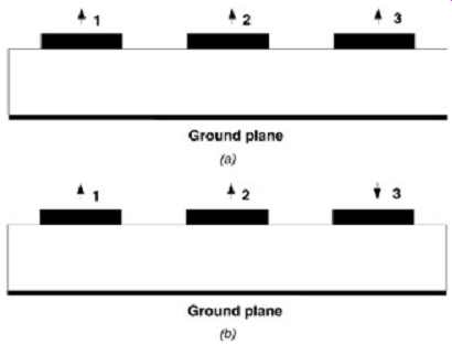
FIG. 12: Example switching pattern: (a) all bits switching in phase; (b)
bits 1 and 2 switching in phase, bit 3 switching 180° out of phase.
If the primary goal is to evaluate this multiconductor system ( FIG. 12a) quickly with a single line, and the target is line 2, the equivalent impedance and time delay per unit length seen by line 2 can be calculated as
(33)
(34)
Example 5: Pattern-Dependent Impedance and Delay.
Assume that the switching pattern of a three-conductor system is such that bits 1 and 2 are switching in phase and bit 3 is switching 180° out of phase, as shown in FIG. 12b (line 2 is still the victim).
-- Even-mode capacitance of conductor 2 with 1 = C22 - C12
-- Odd-mode capacitance of conductor 2 with 3 = C22 + C23
-- Equivalent capacitance of conductor 2 = C22 - C12 + C23
-- Even-mode inductance of conductor 2 with 1 = L22 + L12
-- Odd-mode inductance of conductor 2 with 3 = L22 - L23
-- Equivalent inductance of conductor 2 = L22 + L12 - L23
The equivalent single-conductor model of this multiconductor system would have the following transmission line parameters:
It should be noted that this simplified technique is best used during the design phase of a bus when buffer impedances and line-to-line spacing are being chosen. The reader should also be reminded that this technique is useful only for signals traveling in the same direction.
For crosstalk effects of signals traveling in opposite directions, equivalent circuit models and a circuit simulator must be utilized.
It should also be noted that the SLEM method is only an approximation that is useful for quickly narrowing down the solution space on a design prior to layout. Final simulations should always be done with fully coupled models. Comparison to fully coupled simulations and measurements have shown that the accuracy of the SLEM model (for three lines) is adequate for the cross sections with a spacing/height ratio greater than 1. When this ratio is less than 1, the SLEM approximation should not be used. The method is always accurate, however, for two lines.
POINTS TO REMEMBER
-- When estimating the effect of crosstalk in a system, the nearest neighbors have the greatest effect. The effects of the other lines fall off exponentially.
-- The SLEM method should be used early in the design stage to quickly get a handle on the effect of crosstalk. SLEM is useful because it’s computationally quick. Fully coupled simulations should always be performed on the final design.
-- Common mode (all bits in phase) and differential mode (target bit out of phase) will produce the worst-case impedance and velocity variations.
-- The accuracy of a three-line SLEM model falls off when the edge-to-edge spacing/height (above the ground plane) ratio is less than 1.
7. CROSSTALK TRENDS
As described in Sect. 6, the impedance variations due to crosstalk depend on the magnitude of the mutual capacitance and inductance. In turn, since the mutual parasitics will depend heavily on the cross-sectional geometry of the trace, the impedance variation will also. Lower-impedance traces will tend to exhibit less crosstalk-induced impedance variation than will high-impedance traces for a given dielectric constant. This is because lower impedance traces exhibit heavier coupling to the reference planes (in the form of a higher capacitance, see Section 2). A transmission line that is strongly coupled to the reference planes will simply exhibit less coupling to adjacent traces. Lower-impedance lines are usually achieved either by widening the trace width or using a thinner dielectric. However, there are negative aspects to each of these choices. Wide traces will consume more routing area, and thin dielectrics can be very costly (thin dielectrics tend to have shorts between signal and reference plane layers, so the production yield is low).
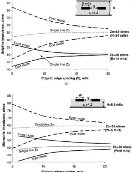
FIG. 13: Variations in impedance as a function of spacing: (a) typical
stripline two conductor system; (b) typical microstrip two-conductor system.
FIG. 13a and b show how even- and odd-mode impedance varies with trace-to-trace spacing. Notice that both the odd- and even-mode impedance values asymptotcally approach the nominal impedance. The target line impedance was calculated with no consideration of the effect of adjacent traces (65 and 50 --). This is usually how impedance calculations are made and it’s how board vendors test (they usually measure an isolated trace on a test coupon). Notice that at small spacing, the single-line impedance is lower than the target. This is because the adjacent traces increase the self-capacitance of the trace and effectively lower its impedance even when they are not active. When they are switching, the full odd- or even-mode impedance is realized. When designing high-trace-density boards, it’s important to account for this effect.
The trace dimensions used to calculate the curves in FIG. 14a and 14b were chosen to approximate real-world values for both 50- and 65-? trace values (both are common in the industry). Notice that the high-impedance traces exhibit significantly more impedance variation than do the lower-impedance traces because the reference planes are much farther in relation to the signal spacing. The mutual parasitics for these cross sections are plotted in FIG. 14. Note that the mutual parasitics drop off exponentially with spacing. Also note that the values of the mutual terms are smaller for the lower impedance trace. The reader should note that these plots are for a simple two-conductor system. Significantly more variation can be expected when the target line is coupled to multiple aggressor nets.
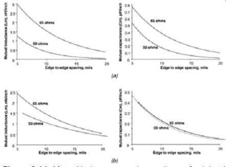
FIG. 14: Mutual inductance and capacitance for (a) stripline in FIG. 13a
and (b) microstrip in FIG. 13b.
POINTS TO REMEMBER
-- Low-impedance line will produce less impedance variation from cross-talk for a given dielectric constant.
-- The impedance of a single line on a board is influenced by the proximity of other traces even when they are not being actively driven.
-- Mutual parasitics fall off exponentially with trace-to-trace spacing.
8. TERMINATION OF ODD- AND EVEN-MODE TRANSMISSION LINE PAIRS
The remaining issue that has not yet been covered is how to terminate a coupled transmission line pair. In most aspects of a design, it’s usually prudent to minimize coupling between all traces. In some designs, however, this is either not possible or it’s beneficial to have a high degree of coupling between two traces. One example where it’s beneficial to have a high amount of coupling between traces is when the system clock on a computer is routed differentially. A differential transmission line consists of two tightly coupled traces that are always propagating in odd mode. The receiving circuitry is either a differential or a single-ended buffer. The input stage of a differential receiver usually consists of a differential pair that triggers at the crossing point of the two signals when the difference between the two signals is zero. Differential transmission lines are beneficial because they tend to exhibit better signal integrity than that of a single trace because they are more immune to noise and EMI is greatly reduced.
8.1. Pi Termination Network
One way to properly terminate a two-line coupled pair and prevent reflection in both the odd and even modes is to use a pi network. This particular termination scheme is useful when differential receivers are used. Refer to FIG. 15. The resistances R1, R2, and R3 must be chosen so that both the even and odd propagation modes will be terminated. First, let's consider even mode, where V1 = V2 = Ve. Since the voltage differences at nodes 1 and 2 will always be equal, no current will flow between these points. Subsequently, R1 and R2 must equal the even-mode impedance. To determine the value of R3, it’s necessary to evaluate the odd-mode propagation. Since V1 and V2 will always be equal but opposite values in the odd mode (V1 = -V2 = V0), R3 can be broken down into two series resistances, each with a value equal to, R3. For odd-mode propagation, the center connection of the two series resistors is a virtual ac ground. Refer to FIG. 16 for a visual representation of the equivalent termination for the odd-mode case. To understand why the middle of the resistor, R3, must be ground for odd-mode propagation, consider a resistor that is constructed from a long piece of resistive material. If a voltage of -1.0 V is applied at one end and a voltage of 1.0 V is applied at the other end, the center of the resistor would have a voltage of 0.0 V. This means that each signal, in odd-mode propagation, is terminated with a value of R1 (or R2), in parallel with R3. The required values of R1 and R3 that may be used to terminate a pair of tightly coupled transmission lines in both even and odd propagation modes are (35), (36).
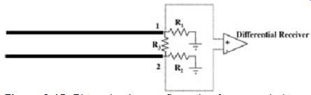
FIG. 15: Pi termination configuration for a coupled transmission line pair.
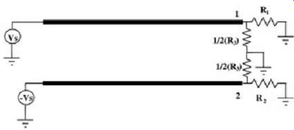
FIG. 16: Equivalent of termination seen in the odd mode with the pi termination
configuration.
It should be noted, however, that if the transmission line pair will always be propagating in one mode (such as in the case of a differential clock line), the middle resistor, R3, is not necessary.
8.2. T Termination Network
Another method of terminating both odd and even modes is a T-network of resistors. Refer to FIG. 17. This particular termination scheme is useful.
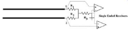
FIG. 17: T termination configuration for a coupled transmission line pair.
FIG. 18: Equivalent of termination seen in the even mode with the T termination
configuration.
...when a differential transmission line pair is used in conjunction with a single-ended receiver.
First, let's consider the termination necessary for the odd mode. Because the voltage at node 1 will always be equal but opposite the voltage at node 2, we can place a virtual ac ground at the center, where R3 is connected. This means that for odd-mode propagation, the lines are effectively terminated in the values of R1 and R2. Therefore, R1 and R2 must be set to a value equal to the odd-mode impedance. Now let's consider the even mode. FIG. 18 shows how two resistors in parallel with a value of 2R3 are used to represent R3. Since no current will flow between points 1 and 2, the resistor R1 or R2 in series with 2R3 must equal the even-mode impedance. The subsequent values for R1, R2, and R3 in a T termination network are (37), (38) of the resistor, R3, must be ground for odd-mode propagation, consider a resistor that is constructed from a long piece of resistive material. If a voltage of -1.0 V is applied at one end and a voltage of 1.0 V is applied at the other end, the center of the resistor would have a voltage of 0.0 V. This means that each signal, in odd-mode propagation, is terminated with a value of R1 (or R2), in parallel with R3. The required values of R1 and R3 that may be used to terminate a pair of tightly coupled transmission lines in both even and odd propagation modes are (35), (36).
It should be noted, however, that if the transmission line pair will always be propagating in one mode (such as in the case of a differential clock line), the middle resistor, R3, is not necessary.
8.2. T Termination Network
Another method of terminating both odd and even modes is a T-network of resistors. Refer to FIG. 17. This particular termination scheme is useful ...
FIG. 17: T termination configuration for a coupled transmission line pair.
FIG. 18: Equivalent of termination seen in the even mode with the T termination
configuration.
... when a differential transmission line pair is used in conjunction with a single-ended receiver.
First, let's consider the termination necessary for the odd mode. Because the voltage at node 1 will always be equal but opposite the voltage at node 2, we can place a virtual ac ground at the center, where R3 is connected. This means that for odd-mode propagation, the lines are effectively terminated in the values of R1 and R2. Therefore, R1 and R2 must be set to a value equal to the odd-mode impedance. Now let's consider the even mode. FIG. 18 shows how two resistors in parallel with a value of 2R3 are used to represent R3. Since no current will flow between points 1 and 2, the resistor R1 or R2 in series with 2R3 must equal the even-mode impedance. The subsequent values for R1, R2, and R3 in a T termination network are (37), (38).
9. MINIMIZATION OF CROSSTALK
Since crosstalk is prevalent in virtually every aspect of a design, and its effects can be quite detrimental to system performance, it’s useful to present some general guidelines to help reduce crosstalk. It should be noted, however, that all these guidelines will have adverse effects on the routability of the printed circuit board.
FIG. 19: Dimensions that influence crosstalk.
Since most circuit board designs are required to fit some predefined aspect ratio (i.e., a motherboard may be required to fit in a standard ATX chassis), a certain degree of crosstalk impact is inevitable. The following guidelines, however, will help the designer limit the negative impact of crosstalk. Refer to FIG. 19 when reading the following list.
1. Widen the spacing S between the lines as much as routing restrictions will allow.
2. Design the transmission line so that the conductor is as close to the ground plane as possible (i.e., minimize H) while achieving the target impedance of the design. This will couple the transmission line tightly to the ground plane and less to adjacent signals.
3. Use differential routing techniques for critical nets, such as the system clock if system design allows.
4. If there is significant coupling between signals on different layers (such as layers M3 and M4), route them orthogonal to each other.
5. If possible, route the signals on a stripline layer or as an embedded microstrip to eliminate velocity variations.
6. Minimize parallel run lengths between signals. Route with short parallel sections and minimize long coupled sections between nets.
7. Place the components on the board to minimize congestion of traces.
8. Use slower edge rates. This, however, should be done with extreme caution. There are several negative consequences associated with using slow edge rates.
10. ADDITIONAL EXAMPLES
This example will build on the additional example in Section 2 and incorporate the effects of crosstalk into the high-speed bus example. Crosstalk often places severe limits on system performance, so it’s important to understand the concepts presented in this Section.
10.1. Problem
Assume that two components, U1 and U2, need to communicate with each other via an 8-bit wide high-speed digital bus. The components are mounted on a standard four-layer motherboard with the stackup shown in FIG. 20. The driving buffers on component U1 have an impedance of 30 ? and a swing of 0 to 2 V. The traces on the printed circuit board (PCB) are required to be 5 in. long with center-to-center spacing of 15 mils and impedance 50 ? (ignoring crosstalk). The relative dielectric constant of the board (er) is 4.0, the transmission line is assumed to be a perfect conductor, and the receiver capacitance is small enough to be ignored. FIG. 21 depicts the circuit topology.
FIG. 20: Cross section of PCB board used in the example.
FIG. 21: Circuit topology.
The transmission line parasitics are:
-- mutual inductance = 0.54 nH/in.
-- mutual capacitance = 0.079 pF/in.
-- self-inductance = 7.13 nH/in.
-- self-capacitance = 2.85 pF/in.
10.2. Goals
- __ Determine the maximum impedance variation on the transmission lines due to crosstalk.
- __ Determine the maximum velocity difference due to crosstalk.
- __ Assuming that the input buffers at component U2 will switch at 1.0 V, determine if the buffer will false trigger due to crosstalk effects.
10.3. Determining the Maximum Crosstalk-Induced Impedance and Velocity Swing
As discussed in Sect. 6.2, the equivalent impedance of a transmission line in a coupled system is dependent on the switching pattern on the adjacent traces. To determine the worst-case impedance swing due to crosstalk, it’s necessary to pick the line in the bus that will experience the most crosstalk. A line in the center of the bus is usually the best choice.
As mentioned earlier in the Section, only the nearest-neighboring lines will contribute the majority of the crosstalk effects. Therefore, the procedures illustrated in previous examples can be used to calculate the impedance variation due to crosstalk. The patterns that produce the worst-case crosstalk effects will always be either common mode or differential mode. In common mode the nets are all switching in phase, and in differential mode the target line is always switching 180° out of phase with the other nets on the bus.
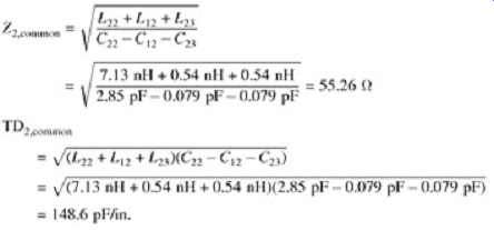
First, let's evaluate the effects of common-mode propagation (all bits switching in phase). Assume that line 2 in FIG. 22 represents a conductor in the middle of the 8-bit bus.
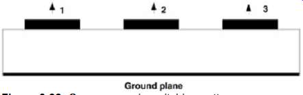
FIG. 22: Common-mode switching pattern.
-- Even-mode capacitance of conductors 2 and 1 = C22 - C12
-- Even-mode capacitance of conductors 2 and 3 = C22 - C23
-- Equivalent capacitance of conductor 2 = C22 - C12 - C23
-- Even-mode inductance of conductors 2 and 1 = L22 + L12
-- Even-mode inductance of conductors 2 and 3 = L22 + L23
-- Equivalent inductance of conductor 2 = L22 + L12 + L23 Therefore,
Now, let's evaluate the effects of differential-mode propagation. Assume that line 2 in FIG. 23 represents a conductor in the middle of the 8-bit bus.
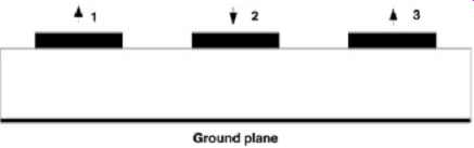
FIG. 23: Differential switching pattern.
-- Odd-mode capacitance of conductors 2 and 1 = C22 + C12
-- Odd-mode capacitance of conductors 2 and 3 = C22 + C23
-- Equivalent capacitance of conductor 2 = C22 + C12 + C23
-- Even-mode inductance of conductors 2 and 1 = L22 - L12
-- Even-mode inductance of conductors 2 and 3 = L22 - L23
-- Equivalent inductance of conductor 2 = L22 - L12 - L23 Therefore,
The velocity and impedance variations due to crosstalk are as follows:
44.8 ? < Z0 < 55.26 ?
135 ps/in. < TD < 148.6 ps/in.
10.4. Determining if Crosstalk Will Induce False Triggers
A false trigger will occur if the signal has severe signal integrity problems. A receiver will trigger at its threshold. Typical CMOS buffers have a threshold voltage at Vcc. If the signal rings back below the threshold level at the receiver, the signal integrity may cause a false trigger. If this happens in a digital system, it could cause a wide variety of problems, ranging from glitches in the data to catastrophic system failure (especially if the false trigger is on a strobe or clock signal).
To determine if the crosstalk will cause a false signal, it’s necessary to evaluate the signal integrity. There are several methods of doing this. The simplest method is to use a simple bounce (i.e., lattice) diagram, such as was used to determine the wave shape of the signal in the Section 2 example. The full bounce diagram, however, is not required. Since the second reflection seen at the receiver will produce the highest magnitude of ringing, all that is required is the voltage level cause by the second reflection as seen at the receiver.
Furthermore, the most ringing will occur when the driver impedance is low and the transmission line impedance is high (see Section 2). Therefore, the worst-case ringing will be achieved when the coupled lines in the bus are propagating in phase with each other (i.e., common mode). The common-mode impedance was calculated above to be 55.2 ?. The signal integrity is calculated using a bounce diagram as shown in FIG. 24.
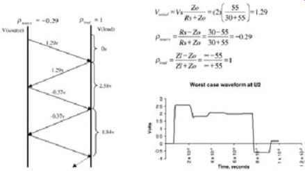
FIG. 24: Calculation of the final waveform.
The signal will ring down to a minimum voltage of 1.84 V. Since the threshold voltage of this buffer was defined to be 1.0 V, and the signal does not ring back down below this value, the signal integrity won’t cause a false triggering of the receiver.