AMAZON multi-meters discounts AMAZON oscilloscope discounts
Modern technology has shown a relentless trend toward higher speeds and smaller form factors. Subsequently, effects previously considered to be negligible and ignored during digital design often become primary design issues. Nonideal effects such as frequency dependent losses, impedance discontinuities, and serpentine effects are just a few of the new variables that must be accounted for in modern designs. Some of these high-frequency effects are very difficult to model and are continuously being researched by universities.
Subsequently, as system designs progress in speed, the engineer not only has to deal with technically difficult issues but must also contend with a significantly greater number of variables. In this Section we address several of the dominant nonideal interconnect issues that must be addressed in modern designs. The focus of this Section is on the high-speed transmission characteristics that have been largely ignored in designs of the past but are critical in modern times. Many of the models presented here have known shortcomings that will, much like the simpler models of previous days, need to be revised sometime in the future. As with any set of models, the user should continually be aware of the approximations and assumptions being made.
1. TRANSMISSION LINE LOSSES
As digital systems evolve and technology pushes for smaller and faster systems, the geometric dimensions of the transmission lines and package components are shrinking.
Smaller dimensions and high-frequency content cause the resistive losses in the transmission line to be exacerbated. Modeling the resistive losses in transmission lines is becoming increasingly important. Resistive losses will affect the performance of a digital system by decreasing the signal amplitude, thus affecting noise margins and slowing edge rates, which in turn affects timing margins. Previously it has been possible to ignore losses on the PCB and in the package because systems operated at slower frequencies. Modern systems, however, require rigorous analysis of losses because they are often a first-order effect that significantly degrades the performance of digital interconnects.
1.1. Conductor DC Losses
As mentioned in Section 2, there is a resistive component in the transmission line model.
This resistive component exists because the conductors used to manufacture the transmission lines on a PCB are not perfect conductors. The loss in microstrip and stripline conductors can be broken down into two components: dc and ac losses. Dc losses are of particular concern in small-geometry conductors, very long lines, and multiload (also known as multidrop) buses. Long copper telecommunication lines, for example, must have repeaters every few miles to receive and retransmit data because of signal degradation.
Additionally, designs of multiprocessor computer systems experience resistive drops that can encroach on logic threshold levels and reduce noise margins.
The DC loss depends primarily on two factors: the resistivity of the conductor and the total area in which the current is flowing. FIG. 1 shows the current distribution on a microstrip line at dc (0 Hz). The current flows through the entire cross section of the conductor, and the resistive loss can be found using the equation (1) ...
...where R is the total resistance of the line, ? the resistivity of the conductor material in ohm meters (the inverse of conductivity), L the length of the line, W the conductor width, t the conductor thickness, and A the cross-sectional area of the signal conductor. The losses in the ground return path in a conventional design are usually negligible at dc because the cross-sectional area is very large compared to the signal line.
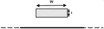
FIG. 1: Microstrip line current density at dc. At dc, current flows through
entire area of the cross section where area = A = Wt.
1.2. Dielectric DC Losses
Since the dielectric materials used in PCBs are not perfect insulators, there is a dc loss associated with the resistive drop across the dielectric material between the signal conductor and the reference plane. The dielectric losses at dc for conventional substrates, however, are usually very negligible and can be ignored. Frequency-dependent dielectric losses are discussed in Sect. 1.4.
1.3. Skin Effect
At low frequencies it’s adequate to use only dc losses in system simulation, however, as the frequency increases, other phenomena that vary with the spectral content of the digital signals begin to dominate. The most prominent of these frequency-dependent variables is the skin effect, so named because at high frequencies, the current flowing in a conductor will migrate toward the periphery or "skin" of the conductor.
Frequency-Dependent Resistance and Inductance.
Skin effect manifests itself primarily as resistance and inductance variations. At low frequencies, the resistance and inductance assume dc values, but as frequency increases, the cross-sectional current distribution in the transmission line becomes nonuniform and moves to the exterior of the conductor. The changing current distribution causes the resistance to increase with the square root of frequency and the total inductance to fall asymptotically toward a static value called the external inductance.
To understand how this happens, imagine a signal traveling on a microstrip transmission line.
The cross section in FIG. 3 shows that a high-frequency signal travels between the signal trace and the reference plane in the form of time-varying electric and magnetic fields and is not contained wholly inside the conductor. When these fields intersect the signal trace or the ground plane conductor, they will penetrate the metal and their amplitudes will be attenuated. The amount of attenuation will depend on the resitivity (or conductivity) of the metal and the frequency content of the signal. The amount of penetration into the metal, known as the skin depth, is usually represented by the symbol d. If the metal is a perfect conductor, there will be no penetration into the metal and the skin depth will be zero. If the metal has a finite conductivity, the portion of the electromagnetic wave that penetrates the metal will be attenuated so that at the skin depth, its amplitude will be decayed by a factor of e-1 of its initial value at the surface. (If the reader is interested in the derivation of the skin depth, any standard electromagnetic text guide should suffice.) This will confine the signal so that approximately 63% of the total current will flow in one skin depth and the current density will decay exponentially into the thickness of the conductor. The physical dimensions of the conductor, of course, modify this current distribution. The skin depth d is calculated with the equation (2) ...
… where ? is the resistivity (the inverse of the conductivity) of the metal, w the angular frequency (2pF), and µ the permeability of free space (in henries per meter) [Johnk, 1988]. (In the rare circumstance that a magnetic metal such as iron or nickel is used, the appropriate permeability should be substituted. This won’t occur except in very unusual situations.) It can be seen that as the frequency increases, the current will be confined to a smaller area, which will increase the resistance, as seen in the dc resistance calculation (1).
This phenomenon also causes variations of the inductance with the frequency. The total inductance of a conductor is caused by magnetic flux produced from the current. Some of the flux is produced from the current in the wire itself. Since at high frequencies the current will be confined primarily to the skin depth, the current will cease to propagate in the center of the conductor. Subsequently, the internal inductance (so named for that portion of current flowing in the internal portion of the conductor) will become negligible and the total inductance will decrease. External inductance is the value calculated when it’s assumed that all the current is flowing on the exterior of the conductor. The total inductance is obtained by summing the external and internal inductances. In most high-speed digital systems, the frequency components of the signals are high enough so that it’s a valid approximation to ignore the frequency dependence of inductance. Therefore, for the remainder of this guide, only the external inductance is considered.
Frequency-Dependent Conductor Losses in a Microstrip.
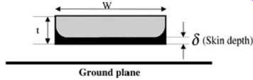
FIG. 2: Current distribution on a microstrip transmission line. 63% of
the current is concentrated in the darkly shaded area due to the skin effect.
By extending the dc resistance equation (1), the frequency dependence of the resistance in a transmission line conductor can be approximated. Frequency-dependent resistance will sometimes be referred to ac resistance in this guide. At low frequencies, the ac resistance will be identical to the dc resistance because the skin depth will be much greater than the thickness of the conductor. The ac resistance will remain approximately equal to the dc resistance until the frequency increases to a point where the skin depth is smaller than the conductor thickness. FIG. 2 depicts the current distribution on a microstrip line at high frequencies. Notice that the current distribution is concentrated on the bottom edge of the transmission line. This is because the fields between the signal line and the ground plane pull the charge to the bottom edge. Also notice that the current distribution curves up the side of the conductor. This is because there is still significant field concentration along the thickness (the t dimension in FIG. 2) of the conductor. The amount of cross-sectional area ...
... in which the current is flowing will become smaller as the frequency increases [see equation (2)].
The losses in the conductor can be approximated using the dc resistance and the skin effect formulas by substituting the skin depth for the conductor thickness: (3a)
Note that the approximation is valid only when the skin depth is smaller than the conductor thickness. Furthermore, equation (3a) is only an approximation because it assumes that all the current is flowing in the skin depth and is presented in this form for instructional purposes only. As this section progresses, more accurate methods of calculating the ac losses will be presented. Notice that when the skin depth equation (2) is inserted into the dc resistance equation, the ac resistance becomes directly proportional to the square root of the frequency F and the resistivity ?. Note that in equation (3a) the length term has been excluded to give the ac resistance units of resistance per unit length.
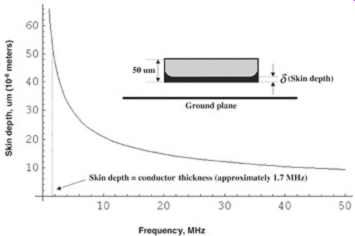
FIG. 3: Skin depth as a function of frequency.
FIG. 3 is a plot of the skin depth versus frequency for a copper conductor. Note that the skin depth is greater than the conductor thickness at frequencies below approximately 1.7 MHz. FIG. 4 is a plot of resistance as a function of frequency for the example copper cross section. Note that the initial portion of the curve is constant at the dc resistance. This section corresponds to frequencies where the skin depth is greater than the conductor thickness.
The curve begins to change with the square root of frequency when the skin depth becomes smaller than the conductor thickness. Although the curve shown in FIG. 4 is not based on an exact model, it’s well suited to help the reader understand the fundamental behavior of skin effect resistance. A good way to match measurements when simulating both the ac and dc resistance of a transmission line in a simulator such as SPICE is to combine Rac and Rdc:
(3b)
The skin effect resistance of the conductor, however, is only one part of the total ac resistance. The portion that is not included in equation (3a) is the resistance of the return current on the reference plane. The return current will flow underneath the signal line in the reference plane and will be concentrated largely in one skin depth and will spread out perpendicular to the trace direction, with the highest amount of current concentrated directly beneath the signal conductor. An approximate current density distribution in the ground plane for a microstrip transmission line is [Johnson and Graham, 1993] (4)
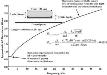
FIG. 4: Ac resistance as a function of frequency.
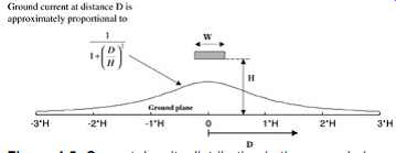
FIG. 5: Current density distribution in the ground plane.
...where Io is the total signal current, D the distance from the trace (see FIG. 5), and H the height above the ground plane. FIG. 5 is a graphical representation of this current density distribution.
An approximation of the effective resistance of the ground plane can be derived using a technique similar to that used to find the ac resistance of the signal conductor. First, since 63% of the current will be confined to one skin depth (d), then for the resistance calculation, the approximation may be made that the ground current flows entirely in one skin depth, as was approximated for the signal conductor ac resistance. Second, the equation (5) ....shows that 79.5% of the current is contained within a distance of ±3H (6H total width) away from the center of the conductor. Thus, the ground return path resistance can be approximated by a conductor of cross section Aground = d × 6H. Substituting this result into equation (1) yields (6) ...
The total ac resistance is the sum of the conductor and ground plane resistance:
(7)
(8)
Equation (8) should be considered a first-order approximation. However, since surface roughness can increase resistance by 10 to 50% (see "Effect of Conductor Surface Roughness" below), equation (8) will probably provide an adequate level of accuracy for most situations.
A more exact formula for the ac resistance of a microstrip can be derived through conformal mapping techniques.
(9)
Equation set (9) was derived using conformal mapping techniques and appears to have excellent agreement with experimental results [Collins, 1992]. These formulas are significantly more cumbersome than (8) but should yield the most accurate results.
Equation (8) will tend to yield resistance values that are larger then those in (9). Often, the slightly larger values given by (8) are used to roughly approximate the additional resistance gained from surface roughness.
Frequency-Dependent Conductor Losses in a Stripline.
In a stripline transmission line, the currents of a high-frequency signal are concentrated in the upper and lower edges of the conductor. The current density will depend on the proximity of the local ground planes. If the stripline is referenced to two ground planes equidistant from the conductor, for example, the current will be divided equally in the upper and lower portions of the conductor, as depicted in FIG. 6. In an offset transmission line, the current densities on the upper and lower edges of the transmission line will depend on the relative distances between the ground planes and the conductor (H1 and H2 in FIG. 6). The current density distributions in each of the return planes in a stripline will be governed by an equation similar to equation (4) and will differ only in the magnitude of the term Io, which will obviously be a function of the respective distances of the reference planes. Thus, the resistance of a stripline can be approximated by the parallel combination of the resistance in the top and bottom portions of the conductor. The resistance equations for the upper and lower sections of the stripline may be obtained by applying equation (8)
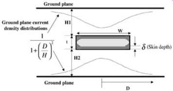
FIG. 6: Current density distribution in a stripline.
... or (9) for the appropriate value of H. These two resistance values must then be taken in parallel to obtain the total resistance for a stripline [see equation (10)]. A good approximation of the ac resistance of a stripline is (10)
where the microstrip resistance values are from equation (8) or (9) evaluated at heights H1 or H2. Refer to FIG. 6 for the relevant dimensions.
Effect of Conductor Surface Roughness.
As discussed earlier, high-frequency signals will experience increased series resistance at high frequency due to migration of the current toward the conductor surface. The formulas for these losses, however, are derived on the assumption of perfectly smooth metal surfaces.
In reality, the metal surfaces will be rough, which will effectively increase the resistance of the material when the mean surface roughness is a significant percentage of the skin depth.
In experimental studies it has been found that high-frequency signals traveling on lines with significant surface roughness exhibit losses that are higher than those calculated with the ideal formulas by as much as 10 to 50%. Because the roughness pattern is random, it’s impossible to predict the skin effect losses exactly. However, by observing the magnitude of the roughness compared to the skin depth, it’s easy to determine if the surface roughness will be of a dominant consequence. FIG. 7 is a drawing of what a stripline in a typical PCB would look like if it were cross-sectioned and examined with a microscope. Note that in this particular case, the surface roughness on the top of the conductor is approximately 0.2 mil (5 µm).
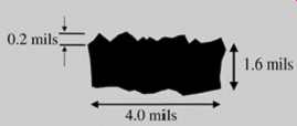
FIG. 7: Cross section of a stripline in a typical PCB, showing surface
roughness.
The roughness of the conductor is usually described as the tooth structure and the magnitude of the surface variations is described as tooth size. For example, the measured tooth size in FIG. 7 is 5 µm. A poll of PCB vendors indicate that typical FR4 boards will have an average tooth size of 4 to 7 µm. Conductor surfaces that are exposed to the etching process will usually have a significantly smaller magnitude of tooth size. Subsequently, the tooth structure with the largest tooth size is usually located on the side of the conductor that is facing the reference plane. Notice that the lower side of the conductor depicted in FIG. 7 has a significantly smaller tooth size, which corresponds to the etched side of the conductor. There are processes that will significantly decrease the amount of surface roughness facing the reference plane; however, they tend to be expensive for high-volume manufacturing purposes at the time of this writing.
The surface roughness will begin to affect the accuracy of the ideal ac resistance equations when the magnitude of the tooth size becomes significant compared to the skin depth. For example, when the frequency reaches 200 MHz, the skin depth in copper will be approximately equal to the surface roughness of a typical PCB. Spectral components above this frequency will experience increasing deviation from the ideal formulas. To gauge the magnitude of the surface roughness, it’s necessary either to perform a cross-sectional measurement such as the one presented in FIG. 7, or to ask the PCB manufacturer for the roughness specification. If the surface roughness is a concern, the ac resistance must be measured.
Frequency-Dependent Properties of Various Metals.
The surface resistance (Rs) is often the parameter used to describe the ac resistance of a given material. The surface resistance is simply the ac resistance as calculated with equations (3) through (9) with the square root of the frequency divided out. Subsequently, the ac resistance will take the form (11)
For the purpose of material property classification, the surface resistance is often calculated for a semi-infinite plane with the length equal to the width (L/W = 1). It’s also assumed that the resistance is calculated in the same manner as in equation (3), where all the current is confined to one skin depth. This approximation is shown in equation (12b). (12)
For a finite area of conductor, the ac resistance is obtained by multiplying Rs (in ohms per square) by the length and the square root of the frequency and dividing by the width. The units of Rac are often reported in ohms per square. Note that the "per square" terminology refers simply to a square of any size (i.e., length = width), since the resistance of one geometric square of board trace at a given thickness is independent of the size of the square.
Thus, the surface resistance can be estimated simply by counting how many squares can be fit geometrically into the area under examination and multiplying that number by Rs times the square root of frequency. The concept of dc resistance per square is illustrated in FIG. 8.
Remember, in interconnect simulation it’s very important to account for both the conductor and the ground return path resistance. Table 4.1 shows the skin effect properties of typical materials.
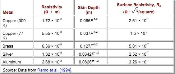
Table 1: Frequency-Dependent Properties of Typical Metals
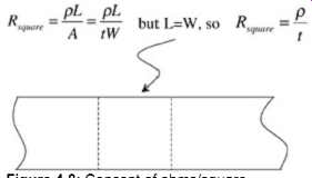
FIG. 8: Concept of ohms/square.
Effect of AC Losses on Signals.
There are two classic implementations of ac losses: those for digital designers and those for microwave designers. The microwave designer is usually interested only in the ac resistance in a frequency-domain simulation. This is easy to implement because most general simulators, such as HSPICE, have a frequency-dependent resistor, which can be made to vary with the root of the frequency [see equation (11)] and used in an equivalent circuit constructed of cascaded LRC segments as in FIG. 4.
The digital engineer, however, has a more difficult problem. Digital signals approximate square waves and are subsequently wide band, which means that they contain many frequency components. This is an important concept to understand. We demonstrate this with the equation [Selby, 1973]
(13)
… which is the Fourier expansion of a periodic square wave at a 50% duty cycle, where F is the frequency and x is the time. A 100-MHz periodic square wave, for example, will be a superposition of an infinite number of sine waves of frequencies that are an odd multiple of the fundamental (i.e., 100 MHz, 300 MHz, 500 MHz, etc.). These components are referred to as harmonics, where n = 1 corresponds to the first harmonic, n = 3 corresponds to the third harmonic, and so on. The skin effect will cause each one of these harmonics to be attenuated with increasing frequency. A real-life signal will, of course, have additional frequency content due to the fact that it’s not a perfect square wave with 50% duty cycle and infinitely fast rise times, as was assumed in equation (13). Notably, as the reader can verify with Fourier techniques, the even harmonics become present in the spectrum if the waveform is not 50% duty cycle. This will be come significant in Section 10.
Since the ac resistance is defined in terms of the frequency domain and digital signals are defined in terms of the time domain, it’s difficult to account correctly for frequency dependent losses in time-domain simulations. Fortunately, many simulators do a good job at this approximation assuming that the user inserts the correct value of Rs. The ac resistance is usually measured with a vector network analyzer (VNA). In the frequency domain, the ac resistance is often characterized by the attenuation factor, a, which is a measure of signal amplitude loss as a function of frequency across a
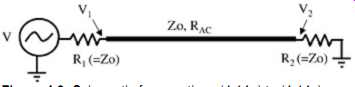
FIG. 9: Schematic for equations (14a) to (14c).
transmission line. In a matched system, such as that depicted in FIG. 9, the attenuation factor can easily be calculated at a single frequency as shown in equations (14a-c), which is based on the voltage divider at the receiver with the ac resistance included in the denominator. If the termination and driver impedance don’t match the characteristic impedance of the transmission line, the voltage-divider method of equation (14c) is not valid because the reflections interfere with the measurement. Since the characteristic impedance of the transmission line does not usually exactly match the internal resistance of the VNA, techniques to eliminate the effect of the reflections must be used. Techniques for measurement of ac losses are described in Section 11.
Equations above: (14a) , (14b) , (14c)
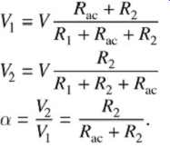
To demonstrate the effect of frequency-dependent losses on a time-domain signal, refer to FIG. 10. FIG. 10a is an ideal trapezoidal wave that represents a digital signal. FIG. 10b is the Fourier transform of the digital signal, showing the frequency spectrum contained in the signal. FIG. 10c is a plot of attenuation versus frequency for a 10-in. long microstrip transmission line. FIG. 10d shows the waveform obtained when the attenuation curve is multiplied by the FFT (fast Fourier transform) curve and inverse FFT is performed. Notice that the wave shape is rounded, the edge rate has decayed, and the amplitude has been attenuated. These effects occur because the high-frequency components of the signal have been attenuated significantly, which eliminates the sharp edges and degrades the edge.
FIG. 10: Effect of frequency-dependent losses on a time-domain signal:
(a) ideal digital pulse (400 MHz periodic, pulse width = 1.25 ns, period
= 2.5 ns); (b) Fourier transform showing frequency components; (c) attenuation
factor versus frequency; (d) effect that frequency-dependent losses have
a time-domain signal. Each simulator will have its own way to implement the
ac resistance. All will require the user to input the surface resistance (Rs)
and either a cross section of the transmission line or the inductance and capacitance
matrix (see Section 2).
1.4. Frequency-Dependent Dielectric Losses
In most designs the dielectric losses can be ignored because the conductor losses are dominant. As frequencies increase, however, this assumption will cease to be true.
Subsequently, it’s important to understand the fundamental mechanisms that cause the dielectric losses to vary with frequency.
When a time-varying electric field is impressed onto a material, any molecules in the material that are polar in nature will tend to align in the direction opposite that of the applied field.
This is called electric polarization. The classical model for dielectric losses, which was inspired by experimental measurement, involves an oscillating system of molecular particles, in which the response to the applied electric fields involves damping mechanisms that change with frequency [Johnk, 1988]. Any frequency variations in the dielectric loss are caused by these mechanisms.
When dielectric losses are accounted for, the dielectric constant of the material becomes complex: (15) where the imaginary portion represents the losses and the real portion is the typical value of the dielectric constant. Since the imaginary portion of equation (15) represents the losses, it’s convenient to think of it as the effective conductivity (i.e., the inverse of the resistivity) of the lossy dielectric.
Subsequently, as shown in any electromagnetics textbook, 1/? = 2pFe" becomes the equivalent loss mechanism, where ? is the effective resistivity of the dielectric material and F is the frequency. Like metals, however, the losses of a dielectric are usually not characterized by its resistivity. The typical method of loss characterization in dielectrics is by the loss tangent [Johnk, 1988]: (16)
where ? is the resistivity of the dielectric. For most practical applications, simulators allow the input of a loss tangent as in equation (16). However, if the designer desires to create an equivalent circuit of a transmission line with LRC segments as in Sect. 3.3, a relationship between tan |dd| and the shunt resistance G in the transmission line model must be established. This relationship is shown as [Collins, 1992] (17) where C11 is the self-capacitance per unit length and F is the frequency. The loss tangent will change with frequency and material properties. FIG. 11 shows the loss tangent for a typical sample of FR4 as a function of frequency.
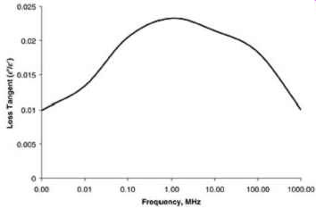
FIG. 11: Frequency variance of the loss tangent in typical FR4 dielectric.
(Adapted from Mumby [1988].)
Example 1: Calculating Losses.
Refer to the stripline cross section depicted in FIG. 6.
Calculate the surface resistivity (Rs) assuming that W = 5 mils, H1 = H2 = 10 mils, t = 0.63 mil, and er = 4.0.
Determine how the resistance will change as a function of the frequency.
Calculate the shunt resistance due to the dielectric losses at 400 MHz.
Calculate the series resistance due to the conductor losses at 400 MHz.
SOLUTION: Equations (9), (10), and (11) are used to calculate the surface resistivity for the transmission line. Initially, the resistance for both the bottom and top portions of the transmission line is calculated assuming the microstrip equations. Then equation (10) is used to determine the stripline resistance. To determine the resistivity, the square root of the frequency is divided out.
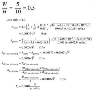
To determine how the resistance will vary with frequency, it’s necessary to determine the frequency at which the skin depth becomes smaller than the conductor thickness. To do so, we examine equation (2), substitute the conductor thickness in place of the skin depth, and solve for the frequency.
Below 17 MHz, the resistance of this conductor is approximately equal to the dc resistance [equation (1)]:
Above 17 MHz, the resistance will vary with the square root of frequency:
Therefore, the resistance at 400 MHz is ...
To calculate G (the shunt resistance between the signal conductor and the ground plane), the self-capacitance of the line is found using the equations from Sect. 3.
The equivalent resistance due to the finite conductivity of the dielectric is calculated using equation (17). The loss tangent at 400 MHz is found from FIG. 11.
Note that the total shunt resistance due to the dielectric losses is almost 15 times larger than the series resistance of the conductor.
2. VARIATIONS IN THE DIELECTRIC CONSTANT
The dielectric constant of the PCB substrate, er, directly affects the signal transmission characteristics of high-speed interconnects. Some of the characteristics that are dependent on er include propagation velocity, characteristic impedance, and crosstalk. The value of er is not always constant for a given material but varies as a function of frequency, temperature, and moisture absorption. Additionally, for a composite material, the material dielectric properties will change as a function of the relative proportions of its components [Mumby, 1988].
The substrate of choice for most PCBs in commercial applications is a composite called FR4, which consists of an epoxy matrix reinforced by a woven glass cloth. This composite features a wide range of thickness and relative compositions of glass and resin.
Consequently, the dielectric properties observed for FR4 laminates can differ substantially from sample to sample. Most vendors will provide a value of er for only one frequency. To ensure a robust digital design that will yield adequate performance over all manufacturing and environmental tolerances, it’s important to consider the variations in the dielectric constant.
A first-order approximation of the dielectric constant of FR4 composite may be calculated as (18)
where ersn and egls is the dielectric constants of the epoxy resin and the woven glass cloth and Vrsn and Vgls are the volume fractions of the resin and glass cloth. The relative volume fractions of glass to resin can change from sample to sample. Subsequently, it’s possible that different layers of a PCB board can be manufactured with samples from different lots of FR4. Subsequently, relatively large variations in the dielectric constant are possible between layers on the same PCB. Measurements have also shown that the dielectric constant of FR4 can vary with frequency and resin content. A typical plot of dielectric constant variations versus frequency for a volume resin fraction of 0.724 is shown in FIG. 12.
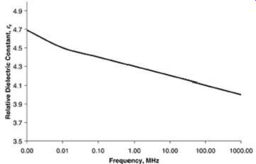
FIG. 12: Dielectric variation with frequency for a typical sample of
FR4. (Adapted from Mumby [1988].)
An approximate equation for the prediction of the relative dielectric constant of FR4 as a function of frequency and resin content is (19).
This relationship is supported by extensive data acquired for FR4 laminates and has been shown to be accurate within a few percent of experimental measurement over the range 1 kHz to 1 GHz. Since this equation was derived empirically, caution should be taken when extrapolating to frequencies above 1 GHz [Mumby, 1988]. It has been determined through experimental measurement that the glass cloth reinforcement experiences no dielectric constant variation in this frequency range; subsequently, the equation is only a function of the frequency and the resin content.
The PCB manufacturer should be able to provide the volume content of the resin. However, if this information is not attainable, it can be estimated as (20) … where Hgls is the total thickness of the glass cloth and H is the total thickness of the dielectric layer. When PCBs are manufactured, the dielectric layers are built up to the desired thickness by stacking several layers of glass cloth and gluing everything together with the epoxy resin. The manufacturer can provide the type and thickness of glass cloth used and the number of layers used, which will yield Hgls. The total layer thickness can either be measured via cross-sectioning techniques or obtained from the manufacturer.
3. SERPENTINE TRACES
When a layout engineer is routing the board, it’s usually impossible to route each net in a perfectly straight line. Board aspect ratios, timing requirements, and real estate limitations inevitably require that the traces be routed in serpentine patterns such as depicted in FIG. 13. Extensive serpentine patterns will probably be encountered when the design specification of a digital system requires all the traces on the PCB to be length equalized and there is limited real estate on the board to do so. Serpentine traces are also often used to fix timing "hold" problems by delaying the data with respect to the clock.
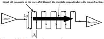
FIG. 13: Example of a serpentine trace.
The effect of a serpentine trace is seen in both the effective propagation delay and the signal integrity. These effects are caused primarily by self-coupling between the parallel sections of transmission line (Lp in FIG. 13). To understand this, imagine a signal propagating down a transmission line. If the trace is serpentined with enough space between parallel sections to eliminate crosstalk effects, the waveform seen at the receiver will behave as if it were propagating down a straight line. However, if significant crosstalk exists between the parallel sections, a portion of the signal will propagate in a path that is perpendicular to the serpentine via the mutual inductance and capacitance as depicted in FIG. 13.
Subsequently, a component of the signal will arrive early, which will affect the signal integrity and the delay. FIG. 14 shows the difference between a 5-in. straight line and a 5-in. serpentine line with 5- and 15-mil spacing. Notice that as the space between the parallel sections is increased (S in Figures 4.13 and 4.14), the waveform approaches the ideal straight-line case. These simulations were performed on buried microstrip lines with a relative dielectric constant of 4.2, which produced a propagation delay of approximately 174 ps/in. (see Section 2). Therefore, if no coupling were present between the parallel sections, the signal would arrive at the receiver in approximately 870 ps for a 5-in. trace. FIG. 14, however, shows components of the signal arriving much earlier than the ideal 870 ps for the serpentined traces. These early components are the portion of the signal that travels perpendicular to the coupled parallel section via the mutual parasitics. Notice that the magnitude of the ledges change significantly for differing degrees of coupling, but the time duration of the ledges remain constant. The duration of the ledges are proportional to the physical length of the coupled sections (Lp) and the voltage magnitude of the ledges depend on the space between parallel sections.
It should be noted that even if the signal integrity impact does not cause a timing problem directly (i.e., the ledges occur outside the threshold region), it can contribute to other problems, such as ISI (which is discussed in Sect. 4).
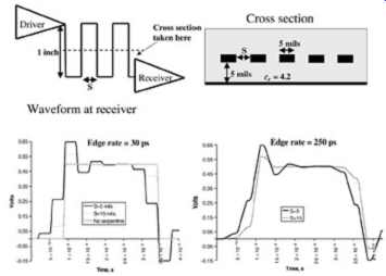
FIG. 14: Effect of a serpentine trace on signal integrity and timing.
RULE OF THUMB: Serpentine Traces
The following guidelines will help minimize the effect of serpentine traces on signal integrity and timing:
-- Make the minimum spacing between parallel sections (S) at least 3H to 4H, where H is the height of the signal conductor above the reference ground plane. This will minimize coupling between parallel sections.
-- Minimize the length of the serpentined sections (Lp) as much as possible. This will reduce the total magnitude of the coupling.
-- Embedded microstrips and striplines exhibit fewer serpentine effects than do microstrip lines.
-- Don’t serpentine clock traces.
4. INTERSYMBOL INTERFERENCE
When a signal is transmitted down a transmission line and the noise on the bus due to reflections, crosstalk, or any other source has not settled completely, the signal launched onto the line will be affected, degrading both the timing and the signal integrity margins. This is referred to as intersymbol interference (ISI) noise. ISI is a major concern in any high speed design, but especially so when the period is smaller than two times the delay of the transmission line. ISI must be analyzed rigorously in system design because it’s often a dominant effect on performance. FIG. 15 shows a graphical example of how ISI can affect timings. Note the timing difference between the ideal waveform and the noisy waveform that begins the transition with unsettled noise on the bus. Left unchecked, this timing difference can be several hundred picoseconds and can consume all available timing margins in a high-speed design.
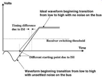
FIG. 15: Effect of ISI on timings.
To capture the full effects of ISI, it’s important to perform many simulations with long pseudorandom bit patterns, and the timings should be taken at each transition. The bit patterns should be chosen so that all system resonances are sufficiently excited and the noise is allowed to settle partially prior to the next transition. To capture most of the timing impacts, however, simulations can be performed with a single periodic bit pattern at the fastest bus period and then at 2× and 3× multiples of the fastest bus period. For example, if the fastest frequency the bus will operate at is 400 MHz, the pulse duration of a single bit will be 1.25 ns. The data pattern should be repeated with pulse durations of 2.5 and 3.75 ns.
This will represent the following data patterns transitioning at the highest bus rate:
-- 010101010101010
-- 001100110011001
-- 000111000111000
The maximum difference in flight time, or flight-time skew between these patterns, produces a first-order approximation of the ISI impact ( Section 9 defines flight time as used in digital system design). This analysis can be completed in a fraction of the time that it takes to perform a similar analysis using long pseudorandom patterns. It must be stressed, however, that the most accurate impact of ISI must be evaluated with long pseudorandom bit patterns.
ISI will also dramatically affect the signal integrity. FIG. 16 shows the effect that different bit patterns have on the wave shape in a system with significant reflections. It’s important to investigate different bit patterns to ensure a robust design. If a signal is switching at the same time that ringback is occurring, for example, the ringback will be masked at one switching rate but won’t be masked for other switching rates, as shown in FIG. 16. FIG. 16 is a very simple example that demonstrates how dramatically the bit pattern can affect the signal integrity. Realistic bus topologies, especially those with multiple loads, will have very complicated ISI dependencies that can devastate a design if not accounted for. In Section 9 we describe methodologies that can account properly for ISI in the design process.
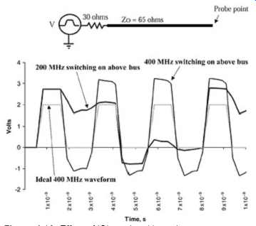
FIG. 16: Effect of ISI on signal integrity.
RULE OF THUMB: ISI
The following guidelines will help to minimize the effect of ISI.
-- Minimize reflections on the bus by avoiding impedance discontinuities and minimizing stub lengths and large parasitics (i.e., from packages, sockets, or connectors).
-- Keep interconnects as short as possible.
-- Avoid tightly coupled serpentine traces.
-- Avoid line lengths that cause signal integrity problems (i.e., ringback, ledges, overshoot) to occur at the same time that the bus can transition.
-- Minimize crosstalk effects.
5. EFFECTS OF 90° BENDS
Virtually every PCB design will exhibit bends in some or all the traces. Thus, how to account for a bend in a transmission line may be important to a simulation. When considering how to model a bend, several things may be considered that may add unnecessary complexity to a model. It has been demonstrated through correlation to empirical measurements that a simple lumped-capacitance model is adequate for most systems. However, the reader should be aware of the limitations of this model to realize when and if the model needs to be revised.
The empirically inspired model for a 90° bend is simply one square of excess capacitance in the transmission line model shown in FIG. 17. This means a capacitance with a value equal to a segment of transmission line equal to its width. This capacitance should be added to a simulated transmission line at the point where the bend occurs. The excess capacitance for a 90° bend for a typical 50- to 65-? line widths is approximated as (21) ...
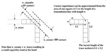
FIG. 17: Extra capacitance from a 90° bend.
...where C11 is the self-capacitance of the line and w is the line width. Although this excess capacitance is typically very small, it can cause problems with wide traces and with large numbers of bends. If this small amount of excess capacitance is a concern, simply rounding the corners to produce a constant width around the bend will virtually eliminate the effect.
Round corners, however, cause problems with many layout tools. Another approach is to chamfer the edge by 45°. The simplest method, however, is to completely avoid the use of 90° bends by using 45° bends instead. The excess capacitance of a 45° bend is significantly smaller than a 90° bend and can be ignored for most applications.
The reader may have noted in equation (21) that the extra capacitance of one full square is more then one might expect if one were to consider the extra capacitance from the extra area as shown in FIG. 18. The reason that empirical measurements may have favored one full square of capacitance rather than the smaller area capacitance shown in FIG. 18 is not clear.
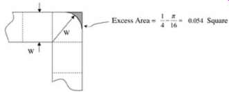
FIG. 18: Excess area of bend. The excess area is less than the 1 square
of empirically inspired excess capacitance for a 90° bend.
There is one more empirically conjectured effect that is worth noting in this section. Some components of the current flow in a transmission line will flow in such a manner that they will deviate from the expected delay based on the layout length. In FIG. 19, consider the dashed line, which might be a component of the current. Since the current cut both corners, that component of the current will arrive at the destination slightly earlier than expected.
Thus, in a system with many bends, the delay may be slightly different than expected. This effect has been seen in laboratory measurements and is mentioned only as a precaution to keep in mind, particularly when two or more separately routed lines with many bends must be of equal delay.
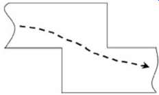
FIG. 19: Some component of the current may hug corners leading to signals
arriving early at destination.
6. EFFECT OF TOPOLOGY
So far in this guide we have covered many issues that deal with an interconnect connecting two components. However, this is not always the case. Often, it’s required that a single driver be connected to two or more receivers. In these cases the topology of the interconnects can affect the system performance dramatically. For example, consider FIG. 20, which is a case where one driver is connected to two receivers. In one case, the impedance of the base (Zo1) is equal to the impedance of the two legs (Zo2). When the signal propagates to the junction, it will see an effective impedance of Zo2/2, resulting in the waveform in the figure that steps up toward the final value. These reflections can be calculated using a lattice diagram similar to that of FIG. 17.
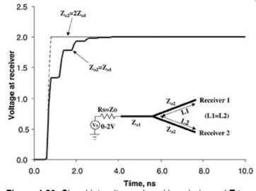
FIG. 20: Signal integrity produced by a balanced T topology.
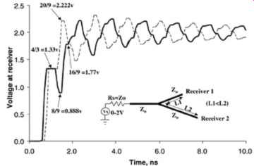
FIG. 21: Signal integrity produced by a unbalanced T topology.
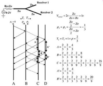
FIG. 22: Lattice diagram of an unbalanced T topology.
When the impedance of the legs are twice the impedance of the base, the effective impedance the signal will see at the junction will be equal to the base; subsequently, there will be no reflections generated. This case, when Zo2 = 2Zo1, is shown in FIG. 20. When the structure is unbalanced, as in the case where one leg is longer than the other, the signal integrity will deteriorate dramatically because the reflections will arrive at the junction at different times. This is shown in FIG. 21. The signal integrity can be calculated with the use of a lattice diagram, although only a masochist would attempt to do so instead of simulating it with a computer. FIG. 22 shows a lattice diagram that calculates the first few reflections in FIG. 21 (the author must be a masochist). Referring to the figure, vertical lines A and B represent the electrical pathway between the driver and the junction, lines B and C represent the path between the junction and receiver 1, and lines B and D represent the pathway between the junction and receiver 2. As more legs are added to the topology, it becomes ever more sensitive to differences in the electrical length of the legs. Furthermore, differences in the loading at each leg will cause similar instabilities.
So what can we learn from this? The answer is symmetry. Whenever a topology is considered, the primary area of concern is symmetry. Make certain that the topology looks symmetric from the point of view of any driving agent. This is usually accomplished by ensuring that the length and the loading are identical for each leg of the topology. The secondary concern in to try and ensure that the impedance discontinuities at the topology junctions are minimized, although this may be impossible in some designs.