AMAZON multi-meters discounts AMAZON oscilloscope discounts
OVERVIEW
A large fraction of this book has explained how to model and understand various elements of a digital system. In this section we explain how to model the driving circuits and incorporate the models into the system interconnect simulations. FIG. 1 shows one example of a buffer tied to a transmission line through a series resistor Rs. In this example, the series resistor Rs plus the impedance of the output buffer Zs should roughly equal the characteristic impedance of the transmission line Zo in order to have matched termination. Accounting for the behavior of various buffer types is the subject of this Section.
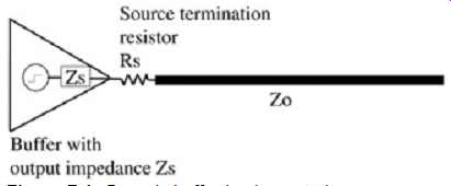
FIG. 1: Generic buffer implementation.
Conceptually, drivers and receivers have largely been treated as fixed-impedance devices up to this point. Although this is useful for deriving the many concepts contained elsewhere in the book, the approximation ignores the fact that the buffer impedance values are dynamic and depend on many variables. In this Section we pick a few buffer types and show how models are derived that can be incorporated into system-level simulations. These concepts can be extended to buffer types not presented here. We do not provide details on actual implementation of models. Instead, we explain some basic concepts, to allow the reader to understand the models and how the simulators may interpret them. This will allow the reader to merge his or her understanding with the function of the simulator.
1. TYPES OF MODELS
There are three general types of models for buffers used for simulation in digital systems: (1) linear model, (2) behavioral model, and (3) full transistor model. In this Section we focus on linear and behavioral models. Full transistor models generally include detailed descriptions of transistors, and are beyond the scope of this book. Several references on transistor details and transistor models are available. The linear model and behavioral model are similar in that they are constructed from curves describing the voltage, current, and time behavior. These models generally can be constructed without proprietary information and are often preferable for this reason. Vendors can distribute buffer models without giving away sensitive information. Also, linear and behavioral models tend to be compatible over a wide variety of simulators, which allows tool independence. The models also run much faster than do full transistor models.
Full transistor models are generally created for some sort of SPICE-like simulator and contain detailed information about the transistors. These models are generally the most accurate, but simulation times and complexity often prohibit their use. Also, the information in the models is not in a format that is readily extractable for understanding the buffer characteristics. Generally, if buffers are completely undefined at the beginning of a design cycle, linear models should be created and simulations performed to determine the desired buffer output impedance and edge rates. The linear buffer model is only valid, however, if a buffer with controlled and roughly linear impedance is desired for the final design. If control of impedance is not important, use of a linear model may not be merited. The information gained from simulations using linear buffer models can later be communicated to buffer designers and used to design actual circuits. More detailed information from either full transistor simulation or measurements can later be used to create more detailed behavioral models. If, however, the buffer to be used in a design already exists, initial simulations should be performed using a behavioral model or a full transistor model.
2. Basic CMOS Output Buffer
The CMOS output buffer is very common in digital designs. Subsequently, it is the buffer chosen to demonstrate the basic principles of buffer modeling.
2.1. Basic Operation
The basic CMOS output buffer is shown in FIG. 2. When the input is high, the output is driven low through the N-type device. When the input is low, the output is driven high through the P-type device. Conceptually, driving devices have been implicitly modeled elsewhere in this book, as shown in FIG. 3. The impedance of the CMOS buffer shown in FIG. 2 is dependent on the instantaneous operating conditions of the device. In other words, the impedance is dynamic. The instantaneous output impedance can be thought of as the slope (or the inverse slope) of the current-voltage (I-V) characteristic curve of the buffer. Some general curves for N and P devices are shown in FIG. 4. The reader will recall the equations governing operation of the CMOS FET transistors as shown in equations (1) through (4) [Sedra and Smith 1991]. The two regions of operation of a FET are the triode region and the saturation region. An N device is in the triode region if vds = vgs - Vt and in the saturation region if vds = vgs - Vt, where Vt is the threshold voltage of the device. A P device is in the triode region if vds = vgs - Vt and the saturation region if vds = vgs - Vt.
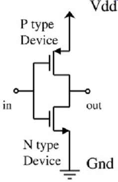
FIG. 2: Basic CMOS output buffer.
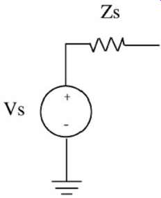
FIG. 3: General method of describing buffers elsewhere in this book.
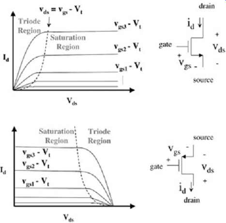
FIG. 4: NMOS and PMOS I-V curves.
For the triode region (see FIG. 4),
(1)
For CMOS devices, K is µCox(W/L), where µ is the mobility of charge carriers (i.e., electrons or holes) in the silicon, Cox the oxide capacitance, and W and L the width and length of the transistor being considered. For the saturation region (see FIG. 4), (2)
…where _ is a positive parameter that accounts for the nonzero slope (i.e., the output impedance) of the curve in the saturation region. The output impedance in the saturation region is defined as:
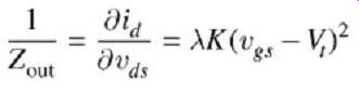 (3)
(3)
This is not the output impedance that should be considered in a model for the basic CMOS buffer, since the CMOS buffer is typically not operated in the saturation region. The output impedance in the saturation region is mentioned here only for completeness and later relevance. Zout in the saturation region is typically very high, and thus _ _ 0 is usually assumed resulting in (4) …for the saturation region.
In order to derive models, let us briefly describe the operation of the basic CMOS buffer.
Consider FIG. 5, which shows the input to the buffer transitioning from low to high with an initial condition of Vdd volts at the output of the buffer. Vdd will be present at the gate of both the P and N devices; thus the N device will have a gate-to-source voltage, Vgs, of Vdd.
The N device will thus be in an "on" condition and will begin to discharge the load to ground.
Subsequently, this transition is often called the pull-down. The initial point (t = 0) on the transistor curve can be found on the Vgs = Vdd curve at Vds = Vdd, as shown in FIG. 6a. At time t = 0, the device operating point will be as shown and the N device will conduct current to discharge the load. As the load is discharged, Vds will decrease and the operating point will shift downward on the curve until the load is discharged to very close to zero volts. The curve for the P device is also shown with Vgs = 0 V. The current conducted by the P device at Vgs = 0 will be equal or very close to zero. The intersection of the P and N curve will be the final, steady-state value of the output when the input to the gate is Vdd.
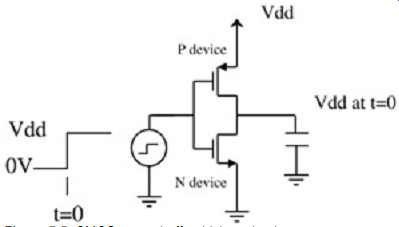
FIG. 5: CMOS output buffer driving a load.
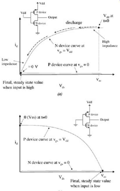
FIG. 6: Operation of the CMOS output buffer when the input voltage is
(a) high and (b) low.
Conversely, when the input to the buffer transitions to zero volts, the N device will turn off and the P device will turn on, which will charge the load to Vdd. This is known as the pull-up transition. The transistor curves shown in FIG. 6b shows the steady-state output value of the buffer when the input is low. The impedance at any point along the discharge is the inverse of the slope of the I-V curve. In FIG. 6a, the impedance varies widely, from a very high value at t = 0 to a lower value as the load discharges. This wide variation in impedance is, of course, not optimal if a controlled range of impedance is desired from the buffer for matching to a transmission line. Ideally, for precisely controlled impedance, the I-V curve will be that of a fixed resistor, which is a straight line, as shown in FIG. 7.
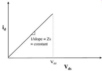
FIG. 7: Ideal I-V curve with a fixed impedance.
Recall that the impedance in the saturation region is very high; thus, operation in this region should be avoided when matched impedance is required. If the buffer is designed for operation primarily within the triode region, the impedance will vary much less, as shown in FIG. 8. Generally, highly linear behavior of the buffer is a desired feature. In early stages of design, when actual buffer curves have not yet been defined, a linear model of the buffer can be used. The information gained from this model can be simulated with a larger system and help in defining the characteristics of the buffer-to-be. In the next section we detail the linear approximation of a buffer.
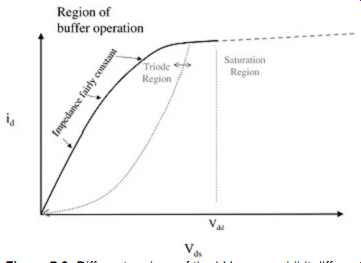
FIG. 8: Different regions of the I-V curve exhibit different impedance
values.
Let us consider the effect on total impedance of the series resistor (either integrated or discrete) as shown in FIG. 1. The variation (with process, temperature, etc.) of the I-V curve of the transistor will vary. This will, of course, affect the impedance. FIG. 9 shows three curves for a transistor at a given Vgs. This variation should be accounted for. Good estimates may be obtained from silicon designers as to the total variation of a given buffer type. Otherwise, assumptions can be made at this point and system simulations can be conducted to determine the allowable constraints. Constraints on the buffer curves for a given design may ultimately be derived from these simulations and communicated back to buffer designers as design rules.
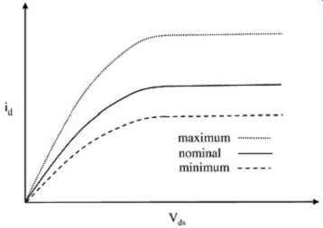
FIG. 9: Variations in the buffer impedance at a constant Vgs due to fabrication
variations and temperature.
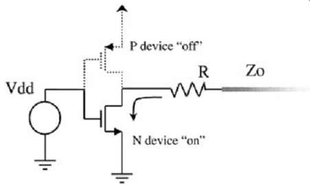
FIG. 10: Buffer in series with a resistor.
To see the effect of a series resistor on the buffer, consider FIG. 10, which shows an N device in series with the resistor. The conclusions derived here will obviously apply to a P device as well. For the total effect of the N device in series with the resistor, the constant impedance of the resistor must be added to the impedance of the transistor. Since impedance is the inverse of the slope of the transistor curve, the extra impedance of the resistor results in a reduction of the slope of the effective buffer curve, as shown in FIG. 11. The larger the resistor, the higher the impedance of the buffer and the more linear the curve. For resistors that are large compared to the low-impedance portion of the transistor, the impedance will be dominated by the value of the resistor and the slope of the I-V curve will be approximately 1/R. Note that with any resistor in series with a buffer, the I-V curve will asymptote at the saturation current of the transistor, since in this condition the transistor is a very high impedance and will dominate the slope of the curve.
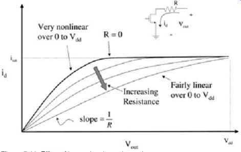
FIG. 11: Effect of increasing the series resistor.
2.2. Linear Modeling of the CMOS Buffer
During the initial phase of a system design, the characteristics of the driving buffers may not be defined. Since the properties of the buffers are one aspect of a design with many codependent variables, some assumptions must be made about the buffers in order to proceed with the design. Typically, a model with a linear I-V curve is chosen for early simulations rather then "guessing" at a more complex behavioral model such as a transistor curve. The linear I-V model is usually appropriate for this stage of design, for three reasons.
First, it is far easier to do multivariable "sweeps" with linear models, due to the simplicity of the model (see Section 9). Second, the linear model leaves nothing to wonder about strange effects from a particular choice of buffer model. This can simplify matters greatly. Third, the linear model has been shown to be fairly accurate when used correctly, so more complex models are not motivated early in the design. Requirements for edge rate and driver strength for the system being defined are easily examined during simulation with linear models, and results may easily be tested. If buffers from an already existing driver are to be used, full models from these buffers should be used instead of linear models. Also, if it is known that a buffer will be used that does not have an approximately linear I-V curve in the region of interest, a linear buffer model is obviously not merited.
The linear model has two features. It has a I-V curve for a pull-up and a pull-down. (Ideally, in a CMOS design, the pull-up and pull-down devices will be very similar.) The model also has a curve defining its switch behavior versus time. The I-V curves are a straight-line (resistor) approximation to a transistor curve. How to pick a good linear fit to a transistor curve will be shown later.
The most simplistic linear model for a CMOS buffer is constructed of a switch, a pull-up resistor, and a pull-down resistor. The values of the resistors are chosen to approximate the impedance of the NMOS and PMOS devices in the intended region of operation. Pull-up and pull-down transitions are made with the switch. The major drawback of this model is that there is usually no edge rate control, because the switch is either in one position or the other, which is a step function. In this case, the edge rates of the model are usually governed by the time constant formed by the output capacitance and the parallel combination of the buffer resistance and the characteristic impedance of the transmission line. FIG. 12a shows this simplistic model. This model is generally only used for "back of the envelope" calculations.
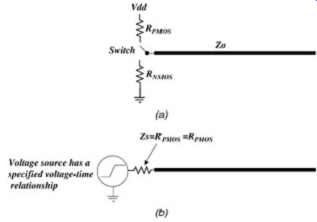
FIG. 12: (a) Most simplistic linear model of a CMOS buffer; (b) another
simplistic linear approach.
Another, rather simplistic linear model is shown in FIG. 12b. This model assumes that the impedance of the pull-up and the pull-down are both equal to the impedance Zs. This modeling approach has the advantage of voltage-time, edge-rate control. The voltage source, Vs, can be specified in SPICE-like simulators to transition from 0 to Vdd in a specified amount of time. Furthermore, most simulators allow the creation of a piecewise-linear voltage-time transition so that specific edge shapes can be mimicked.
A more complete linear model would assume separate linear I-V curves for the pull-up and pull-down devices and have separate curves that describe how the voltage sources will switch from low to high and from high to low. In this book, these curves are known as switch time curves. An even more complete model would include two switch-time curves for the pull-up device and two switch-time curves for the pull-down device. This is because each device must be turned on and turned off. An example model for a pull-up and a pull-down device of a basic CMOS buffer is shown in FIG. 13. The curves shown in FIG. 13 are input into the simulator. Some simulators assume an edge shape and require the user to input only the impedance and the turn-on and turn-off times of the pull-up and the pull-down.
Although various simulators may interpret these curves differently, they are often interpreted as explained below.
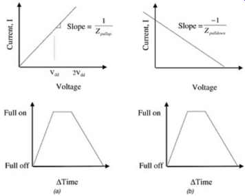
FIG. 13: Behavioral linear model: (a) pull-down; (b) pull-up.
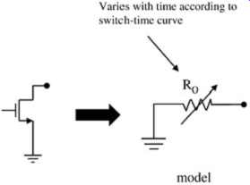
FIG. 14: Basic functionality of linear-behavioral model.
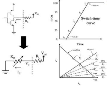
FIG. 15: Interpretation of a linear-behavioral model.
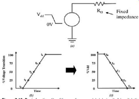
FIG. 16: Basic functionality of linear-linear model: (a) circuit; (b)
switch-time curve; (c) pull-down curve.
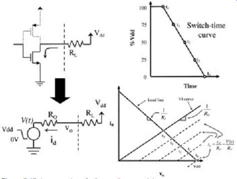
FIG. 17: Interpretation of a linear-linear model.
Generally, the switch-time curve defines how quickly the impedance, Rout, approaches the value in the I-V curve when the device is turning on, as shown in FIG. 14. Basically, the switch-time curve defines how quickly the switch turns on to its full value. When the model is interpreted in this fashion, it will be referred to here as a linear-behavioral model. As shown in FIG. 15, the varying impedance of the device causes the instantaneous operating point to "climb" up the load curve. This is similar to the behavior of a transistor as Vgs increases and the device is transitioning to successively larger, lower impedance Vgs curves as the gate voltage increases.
It should be mentioned that some simulators might interpret the I-V and switch-time curves as the model shown in FIG. 16. In the figure, the switch-time curve is interpreted as a voltage-time curve and is included in the model as a voltage source. The impedance of the model is fixed as the impedance of the I-V curve input into the model. When the model is interpreted in this fashion, it will be referred to here as the linear-linear model. The linear- linear model is likely to be the model used internal to the simulator if the simulation is run in the frequency domain rather than in time domain. To compare this with the variable impedance linear behavioral model, compare Figures 15 and 17. It can be seen that the location of the points labeled t0 through t4 will be slightly different depending on whether the model is interpreted as a linear-linear model or a linear-behavioral model. Also, the linear-linear model can give different results than the linear-behavioral model when considering termination issues. For instance, if Ro = Zo, a reflection terminating at the driver will be matched according to the linear-linear model even when the driver is transitioning.
For the linear-behavioral model, the impedance during the switching interval is dynamic, and thus a reflection arriving during a transition may not be perfectly terminated.
The straight line used to approximate a transistor curve for linear models should be constructed as shown in FIG. 18. The line is defined by two points, one point the zero current point and the other the point where the transistor curve is expected to cross Vdd/2, which is generally the threshold voltage at which receivers define the time location of the edge. Also, as shown, lines should be constructed for the nominal, minimum, and maximum expected curve characteristics to account for variation with temperature, silicon process, and so on. Often, prior to the design of the buffer, the system engineer will perform many simulations with linear buffers that will place limitations on the amount of variation, as we elaborate in Section 9.
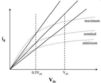
FIG. 18: Measuring the impedance of an I-V curve.
Limitations of the Linear Buffer Model.
Although the linear buffer is generally intended for use only in the initial stages of a design cycle, certain limitations should be kept in mind. First, as mentioned before, if a buffer with very nonlinear behavior will be implemented in the final design, the linear buffer will yield very inaccurate results, due to the inability to fit a line to the behavior of the buffer. Second, actual edge shapes and rise and fall times simulated with the linear buffer will not yield the exact results that will be expected in the final system. Finally, errors induced by the use of the linear model can go unnoticed until very late in the design cycle, when more complex models are used.
To determine the accuracy of the linear approximation, a Bergeron diagram may be used (see Section 2). FIG. 19a and b show a Bergeron diagram of a CMOS output driver in a high state (the PMOS is on). If the buffer is driving a transmission line with an impedance of Zo, the Bergeron diagram will predict the voltages at the source due to the reflections on the net. The validity of a linear model approximation can be judged by observing the intersections on the I-V curve. FIG. 19a shows an example where the voltages from the reflections always intersect the I-V curve in the linear portion. Subsequently, the linear I-V curve (shown as a dotted line) will be adequate when the buffer is driving a transmission line with an impedance of Zo. FIG. 19b shows an example where a linear approximation is not adequate because some voltages from the reflections will occur on the nonlinear portion of the I-V curve. Obviously, approximating the interconnect with only one impedance (Zo) may not be realistic because packages and sockets also introduce discontinuities; however, it is adequate for first-order approximations. This technique may also be useful when specifying buffer characteristics to a silicon designer.
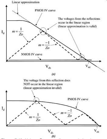
FIG. 19: Using a Bergeron diagram to judge the accuracy of a linear buffer
approximation: (a) valid case; (b) invalid case.
2.3. Behavioral Modeling of the Basic CMOS Buffer
The models shown here are similar to the linear-behavioral models in Section 2.2. The difference is that these models have I-V curves that mimic the transistor curves instead of approximating it with a straight line. Since these models are defined by a transistor curve and a curve for the time behavior, and are not defined by detailed transistor data such as used in a traditional SPICE model, these models are particularly useful when communicating between different companies. This is because a model can be created that does not contain detailed information about silicon processes and other proprietary information.
A behavioral model consists of an I-V curve and a time curve just as in the linear- behavioral models already discussed. This transistor curve should generally be based on known device characteristics. These characteristics may be supplied by the designer or provided by the vendor. Often, early simulations will be performed using one of the linear models in Section 2.2 to determine necessary requirements. The results of the linear simulations may be given to circuit designers or vendors as the initial design targets to create real buffers. Then simulated data based on actual transistor designs (or measured data on the devices) can be used to create a behavioral model.
The structure of a behavioral model is shown in FIG. 20. For each transistor in the model, an I-V curve and a V-T curve is given for both the turn-on and turn-off cycles. The V-T curves are the shape of the actual voltage waveforms driven into an assumed load. The assumed load used in constructing the model does not have to correspond to the physical load that is expected in a system. The simulator takes as input the load used to construct the model and adjusts the model to different load conditions. However, there may be increased accuracy if the load used to construct the model is similar to the load present in the system.
Typically, a load of 50 ohm is chosen; however, other loads can be used to construct the model.
Since a pull-up device, for instance, has no capacity to pull down the output, the turn-off V-T curve is constructed from assuming a pull-down load even if no such load exists in the system. FIG. 21 shows some assumed loads used to construct both the V-T curves for both the pull-up and pull-down devices in a CMOS buffer.
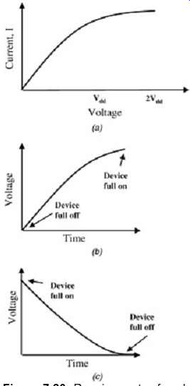
FIG. 20: Requirements of each device (PMOS and NMOS) in a behavioral
model: (a) V-I curve; (b) V-T curve (turn-on); (c) V-T curve (turn-off).
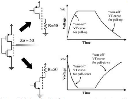
FIG. 21: Creating the V-T curves in a behavioral model.
Generally, the simulator will construct intermediate I-V curves other then the input I-V curve to be used during voltage transitions. The intermediate curves will be chosen such that the time behavior during the transition will mimic the V-T curve input to the model. This behavior is illustrated in FIG. 22. Note in the V-T curve shown in FIG. 22 that there is no data point near the threshold (generally, Vdd/2) at which timing is measured. This may induce a timing inaccuracy, depending on how the simulator (or the model maker) extrapolated points on the V-T curve near the threshold. Generally, models should be defined with at least one point at or near the timing threshold.
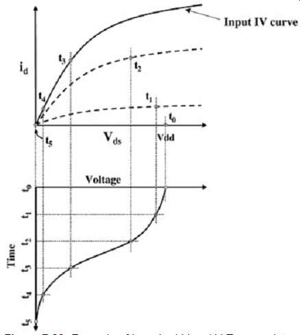
FIG. 22: Example of how the I-V and V-T curves interact.
The I-V and V-T curves used to construct the model can be created from actual silicon measurements or from simulations with full transistor models. In either case, the question arises as to what effects to include in the model. For instance, if a V-T curve is determined directly from measurement of a device that has capacitance present at the output node, the capacitance will obviously affect the shape of the V-T curve measured. This will result in the capacitance being virtually included in the model through its effect on the V-T behavior. If the capacitance under question will actually be present in a physical system, such as on-die capacitance and package capacitance, this has no effect on the driving characteristics of the buffer. However, if the capacitance is embedded in the V-T curve in such a manner, the capacitance will not be modeled properly when the driver node is receiving a voltage waveform such as a reflection. For this reason it is preferable to create the V-T curve with as little capacitance as possible at the output node and then add the capacitance back into the final model as a lumped element. Some capacitance cannot easily be subtracted from the model, particularly if the models are created from direct measurement.
As a final note, it should be mentioned that the behavioral model should be constructed with an I-V curve extending in voltage far beyond the expected operation of the device. This accounts for system effects such as a large overshoot. Typically, if the model is anticipated to be used from 0 to Vdd, the I-V curve of the model should be extended from -Vdd to 2Vdd to account for worst-case theoretical maximums.
3. OUTPUT BUFFERS THAT OPERATE IN THE SATURATION REGION
It was mentioned in 2 (above) that driver capacitance must be considered carefully when creating a behavioral model, particularly for conditions in which the buffer will receive reflections from the system at the output. Buffers that operate solely in the saturation region of the transistor and thus have very high impedance output are finding growing application in high-speed digital applications. Depending on implementation, these buffers are particularly sensitive to capacitance at the output. If capacitance is modeled incorrectly, simulations can yield drastically incorrect results. The impedance of the output is shown in FIG. 23.
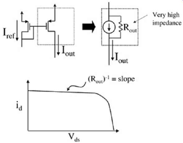 FIG. 23: Example of a buffer that operates in the saturation region.
To see the dependence on output capacitance, consider FIG. 24. If a high-impedance
buffer is terminated at the source end of the transmission line, the termination
will probably be a shunt resistor. Thus the capacitance at the output
of the buffer can be connected directly to the transmission line. Thus,
the capacitance at the output node affects two things.
FIG. 23: Example of a buffer that operates in the saturation region.
To see the dependence on output capacitance, consider FIG. 24. If a high-impedance
buffer is terminated at the source end of the transmission line, the termination
will probably be a shunt resistor. Thus the capacitance at the output
of the buffer can be connected directly to the transmission line. Thus,
the capacitance at the output node affects two things.
First, it affects how fast the voltage on the line changes if the current is shut off completely.
In other words, the minimum fall time possible at the output depends on the size of the capacitor. Additionally, the capacitance can have a strong effect on the termination because the capacitance will appear initially as a low-impedance device to a waveform arriving at the driver (until it is charged up), which could make the termination ineffective. There are several methods to contend with both of the items noted above. The point made here is simply that the capacitance must be modeled correctly to avoid misleading results when simulating with this type of buffer. As much capacitance as possible should be removed from the device when creating the V-T curve for a buffer of this type. This capacitance must then be placed back into the model as a lumped element.
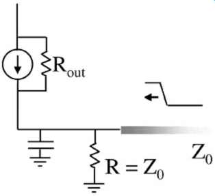
FIG. 24: The output capacitance must be modeled correctly.
4. CONCLUSIONS
A wide variety of buffer types are encountered in digital systems. No attempt has been made to catalog the various types here. However, the same basic concepts outlined in the example buffers of this Section can be used to form linear or behavioral models of any general buffer type. One continuing standard started in the 1990s for behavioral models is known as IBIS (I/O Buffer Information Specification). Information on this model format is widely available. Many simulation tool vendors support this format. Behavioral models can also be created for inputs; however, modeling inputs to buffers is generally not nearly as critical as the drive characteristics.