AMAZON multi-meters discounts AMAZON oscilloscope discounts
OVERVIEW
We have now covered everything that is needed to model a signal propagating from one component to another. We have covered the details of predicting signal integrity variations and estimating timing impacts caused by a plethora of nonideal high-speed phenomenon.
However, this is not sufficient to properly design a digital system. The next step is to coordinate the system so that the individual components can talk to each other. This involves timing the clocks or component strobes so that they can latch in the data at the correct time so that the setup- and hold-time requirements of the receiving components are not violated.
In this Section we describe the basic timing equations for common-clock and source synchronous bus architectures. The timing equations will allow the engineer to track each timing component that affects system performance, set design targets, calculate maximum bus speeds, and compute timing margins.
1. COMMON-CLOCK TIMING
In a common-clock timing scheme, a single clock is shared by driving and receiving agents on a bus. FIG. 1 depicts a common-clock front-side bus similar to some personal computer designs (a front-side bus is the interface between the processor and the chipset). This example depicts the case when the processor is sending a bit of data to the chipset.
The internal latches, which are located at each I/O cell, are shown. A complete data transfer requires two clock pulses, one to latch the data into the driving flip-flop and one to latch the data into the receiving flip-flop. A data transfer occurs in the following sequence:
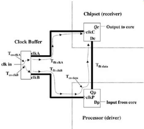
FIG. 1: Block diagram of a common-clock bus.
1. The processor core provides the necessary data at the input of the processor flip-flop (Dp).
2. System clock edge 1 (clk in) is transmitted through the clock buffer and propagates down a transmission line and latches that data from Dp to the output Qp at the processor.
3. The signal on Qp propagates down the line to Dc and is latched in by clock edge 2. The data is then available to the core of the chipset.
Based on the foregoing sequence, a few fundamental conclusions can be made. First, the delay of the circuitry and the transmission lines must be smaller than the cycle time. This is because each time a signal is transmitted from one component to another, it requires two clock edges: the first to latch the data at the processor to the output buffer (Qp), and the second to latch the data at the input of the chipset receiver flip-flop into the core. This places an absolute theoretical limit on the maximum frequency that a common-clock bus can operate. The limitation stems from the total delay of the circuitry and the PCB traces, which must remain less than the delay of one clock cycle. To design a common-clock bus, each of these delays must be accounted for and the setup and hold requirements of the receiver, which are the minimum times that data must be held before and after a clock to ensure correct latching, must be satisfied.
1.1. Common-Clock Timing Equations
To derive the timing equations for a common-clock bus, refer to the timing diagram in FIG. 2. Each of the arrows represents a delay in the system and is labeled in FIG. 1. The solid lines represent the timing loop used to derive the equation for the setup margin, and the dashed lines represent the loop used for the hold margin. How to use the timing loop to construct timing equations will become evident shortly.
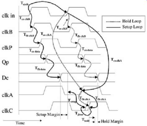
FIG. 2: Timing diagram of a common-clock bus.
The delays are separated into three groups: Tco's, flight times, and clock jitter. The Tco (time from clock to output) is simply the time it takes for a data bit to appear at the output of a latch or a buffer once it has been clocked in. The flight times, Tflt, are simply the delays of the transmission lines on the PCB. Clock jitter, Tjitter, generally refers to the cycle-to-cycle variations of the clock period. Period jitter, for instance, will cause the period of the clock to vary from cycle to cycle, which will affect the timing of the clock edge. For the purposes here, jitter will be considered as a variation that may cause the clock to exhibit a temporary change in clock period.
Setup Timings.
To latch a signal into a component, it is necessary that the data signal arrive prior to the clock. The receiver setup time dictates how long the data must be valid before it can be clocked in. In a common-clock scenario, the data are latched to the output of the driver with one clock edge and latched into the receiver with the next clock edge. This means that the sum of the circuit and transmission line delays in the data path must be small enough so that the data signal will arrive at the receiver (Dc) sufficiently prior to the clock signal (clkC). To ensure this, we must determine the delays of the clock and the data signals arriving at the receiver and ensure that the receiver's setup time has been satisfied. Any extra time in excess of the required setup time is the setup margin.
Refer to the solid arrows in the timing diagram of FIG. 2. The timing diagram depicts the relationship between the data signal and the clocks both at the driver and receiver. The arrows represent the various circuit and transmission line delays in the data and clock paths.
The solid arrows form a loop, which is known as the setup timing loop. The left-hand portion of the loop represents the total delay from the first clock edge to data arriving at the input of the receiver (Dc). The right-hand side of the loop represents the total delay of the receiver clock.
To derive the setup equation, each side of the setup loop must be examined. First, let's examine the total delay from the first clock edge to data arriving at the input of the receiver.
The delay is shown as (see FIG. 1)
(1)
… where Tco clkB is the clock-to-output delay of the clock buffer, Tflt clkB the propagation delay of the signal traveling on the PCB trace from the clock chip to the driving component, Tco data the clock-to-output circuit delay of the driver, and Tflt data the propagation delay of the PCB trace from the driver to the receiver.
Now let's examine the total delay of the clock path to the receiver referenced to the first clock edge. This delay is represented by the solid lines on the right-hand side of the setup loop in FIG. 2. The delay is shown as (2)
… where Tcycle is the cycle time or period of the clock, Tco clkA the clock-to-output delay of the clock buffer, Tflt clkA the propagation delay of the signal traveling on the PCB trace from the clock chip to the receiving component, and Tjitter the cycle-to-cycle period variation. The jitter term is chosen to be negative because it produces the worst-case setup margin, as will be evident in the final equation.
The timing margin is calculated by subtracting equation (1) from (2) and comparing the difference to the setup time required for the receiver. The difference is the setup time margin: (3)
To design a system, it is useful to break equation (3) into circuit and PCB delays, as in equations (4) through (8)
(4)
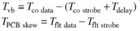
The output clock buffer skew is defined as (5)
This is usually specified in the component data sheet. The PCB flight-time skew for the clock traces is defined as
(6)
Subsequently, the most useful form of the setup margin equation is (7)
A common-clock design will function correctly only if the setup margin is greater than or equal to zero. The easiest way to compensate for a setup timing violation is to lengthen the clock trace for the receiver, shorten the clock trace to the driver, and/or shorten the data trace between the driver and receiver flip-flop.
Hold Timings.
To latch a signal into the receiver successfully, it is necessary that the data signal remain valid at the input pin long enough to ensure that the data can be clocked in without error.
This minimum time is called the hold time. In a common-clock bus design, all the circuit and transmission line delays must be accounted for to ensure proper timing relationships to satisfy the hold-time requirements at the receiver. However, even though the second edge in a common clock transaction latches in the data at the receiver flip-flop, it also initiates the next transfer of information by latching data to the output of the driver flip-flop. Subsequently, the hold timing equations must also ensure that the valid data are latched into the receiver before the next data bit arrives. This requires that the delay of the clock path plus the component hold time be less than the delay of the data path. It is basically a race to see which signal can arrive at the receiver first, the new data signal or the clock signal.
To derive the hold-time equation, refer to the dashed arrows in FIG. 2. The delay of the receiver clock and the delay of the next data transaction must be compared to ensure that the data are properly latched into the receiver before the next data signal arrives at the receiver pin. The clock and data delays are calculated as (8)
(9)
Notice that neither the cycle time nor the clock jitter are included in equation (9). This is because the hold time does not depend on the cycle time, and clock jitter is defined as cycle to-cycle period variations. Since the clock cycle time is not needed to calculate hold margin, jitter is not included.
The subsequent hold-time margin is calculated as (10)
If the substitutions of equations (5) and (6) are made, the useful equation for design is (11)
RULES OF THUMB: Common-Clock Bus Design
---Common-clock techniques are generally adequate for medium-speed buses with frequencies below 200 to 300 MHz. Above this frequency, other signaling techniques, such as source synchronous (introduced in the next section), should be used.
---The component delays and the delays of the PCB traces place a hard theoretical limit on the maximum speed a common-clock bus can operate. Subsequently, a maximum limit is placed on the lengths of the PCB traces.
---Trace propagation delays are governed by trace length. Trace lengths are often governed by the thermal solution. As speeds increase, heat sinks get larger and force components farther away from each other, which limit the speed of a common-clock bus design.
2. SOURCE SYNCHRONOUS TIMING
Source synchronous timing is a technique where the strobe or clock is sent from the driver chip instead of a separate clock source. The data bit is transmitted to the receiver, and a short time later, a strobe is sent to latch the data into the receiver. FIG. 3 depicts an example of a source synchronous bus.
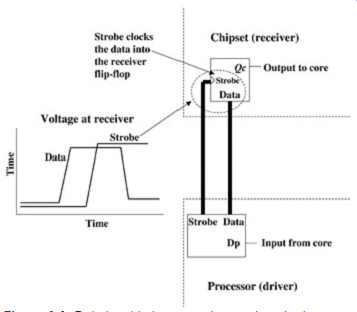
FIG. 3: Relationship between data and strobe in a source synchronous
clock bus. This has several advantages over a common clock. The major
benefit is a significant increase in maximum bus speed. Since the strobe
and data are sent from the same source, flight time is theoretically no
longer a consideration in the equation. Unlike a common clock, where the
maximum bus frequency is governed by the circuit and transmission line
delays, there is no theoretical frequency limit on a source synchronous
bus. There are, however, many practical frequency limitations, which are
a manifestation of all the nonideal effects discussed throughout this
book. To understand the limitations of a source synchronous bus, it is
important to keep in mind that the setup and hold requirements of the
receiver must still be met to ensure proper operation. For example, assume
that the data are transmitted onto the PCB trace 1 ns prior to the strobe
and that the receiver requires a 500 ps setup window.
As long as the delay of the data signal is not more than 500 ps longer than that of the strobe, the signal will be captured at the receiver. Thus, the source synchronous design depends on the delay difference between the data and strobe rather than on the absolute delay of the data signal as in common-clock signaling. The difference in the data and strobe delays depend on numerous factors, such as simultaneous switching noise, trace lengths, trace impedance, signal integrity, and buffer characteristics.
FIG. 4 shows a block diagram of the circuitry and the source synchronous timing path.
The timing path starts at the flip-flop of the transmitting agent and ends at the flip-flop of the receiving agent. Note that the strobe signal is used as the clock input of the receiver flip-flop.
The input to the driver flip-flops is generated by the core circuitry. The strobe pattern is usually produced from an internal state machine. The bus clock is generated from a phase locked loop (PLL) and is usually a multiple of the system clock such as the clock driver typically found on a computer motherboard. For a source synchronous bus to operate properly, the transmission of the strobe must be timed so that both setup and hold requirements of the receiver latch are satisfied. The delay cell in the block diagram achieves this. The delay can be implemented in several ways. Sometimes a state machine is used to clock the data flip-flop on one bus clock pulse and the strobe on the next. Other times the data is clocked off the rising edge of the bus clock and the strobe is clocked off the falling edge. The delay cell shown in the block diagram is simply the most generic way of depicting the required offset between data and strobe.
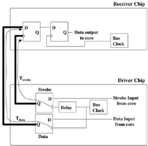
FIG. 4: Block diagram of a source synchronous bus.
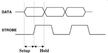
FIG. 5: Setup and hold times in a source synchronous bus.
The ideal delay between data and strobe signals depends on the specific circuitry. Typically, however, the ideal offset is 90 assuming a 50% duty cycle. FIG. 5 depicts a typical data and strobe relationship in a source synchronous bus design.
2.1. Source Synchronous Timing Equations
To derive the timing equation for a source synchronous bus, it is necessary to calculate the difference in delay for the data and the strobe path. FIG. 6 depicts a timing diagram for the simplest implementation of a source synchronous bus. In this particular example, each data transaction requires two clock pulses, the first to clock the data flip-flop at the driver and the second to clock the strobe. Again, both the setup and hold margins must be greater than or equal to zero to guarantee proper timings between components.
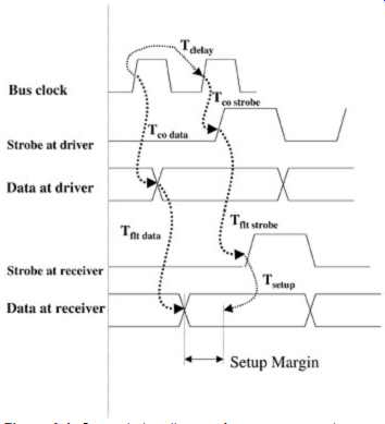
FIG. 6: Setup timing diagram for a source synchronous bus.
Setup Timings.
To derive the timing equations, the delay of the data and strobe paths must be calculated as (12)
(13)
…where Tdelay is the offset between data and strobe. The setup margin is calculated by subtracting (12) from (13) and comparing the difference to the receivers required setup time as in
(14)
…where Tco strobe is the clock-to-output delay of the strobe flip-flop, Tflt strobe the propagation delay of the strobe PCB trace from the driver to receiver, Tco data the clock-to-output delay of the driver flip-flop, Tflt data the propagation delay of the data PCB trace from the driver to the receiver, and Tdelay the delay between data and strobe clocking. In this example, the delay is one clock period. It is left as a delay so that the equations will be generic. The timing diagram is shown in FIG. 6.
To simplify the equation, a few terms need to be defined.
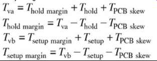
(15)
(16)
Tvb, the "valid before" time, refers to the time before the strobe occurs when the data will be valid. TPCB skew is the difference in flight times between data and strobe signals. Note that this term actually represents the total skew from silicon pad at the driver to silicon pad at the receiver, including all packages, sockets, and every other attribute that can change the delay of the signal. It is not only the delay skew due to PCB trace mismatches; do not be confused by the name.
The simplified equation for setup margin is… (17)
Note that the quantity Tvb is negative. This is because the standard way of calculating skews in a source synchronous design is data minus strobe, and to satisfy setup requirements, the data must arrive at the receiver prior to the strobe. Subsequently, in a working design, (15) will always be negative. The negative sign in (17) is required to calculate a positive margin.
Hold Timings.
The hold-time margin is calculated in the same manner as the setup time, except that we compare the delay between the first strobe cycle and the second data transition. Subtracting the delay of the strobe from the delay of the second data transition and comparing the difference to the receivers hold-time requirement derives (18)
The timing diagram is shown in FIG. 7. Again, to simplify the equation to a useful form, equations (19) and (16) are used. Tva is the "valid after" time and refers to the time after the strobe for which the data signal is still valid.
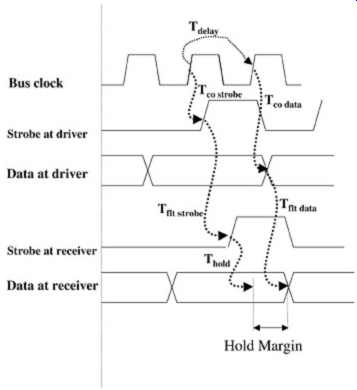
FIG. 7: Hold timing diagram for a source synchronous bus. (19)
The simplified equation for hold margin is (20).
Again, note that the components of the above equations represent the total skew from silicon pad at the driver to silicon pad at the receiver, including all packages, sockets, and all other attributes that can change the delay of the signal.
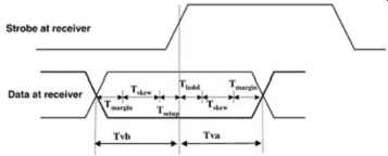
FIG. 8: Calculating the setup and hold margins using an eye diagram for
a source synchronous bus.
2.2. Deriving Source Synchronous Timing Equations from an Eye Diagram
A convenient graphical method to analyze timings is known as an eye diagram. FIG. 8 depicts an idealized eye diagram of the data and strobe at the receiver. It is easy to equate Tva and Tvb to the sum of the skew, hold/setup time, and the margins. The components can then be rearranged to yield the proper equations. This point of view gives more insight into source synchronous timings. The equations derived from the eye are identical to those derived from the timing diagrams. Equations (22) and (24) are the final equations for source synchronous setup and hold margin. Note that the sign convention of Tvb in equation (24) is reversed from the sign convention used in (17). This is done to better fit the graphical representation as applied in the eye diagram.
(21)
(22)
(23)
(24)
RULES OF THUMB: Source Synchronous Timings
---There is no theoretical limit on the maximum bus speed.
---Bus speed is a function of the difference in delay (skew) between data and strobe.
---Nonideal effects cause unwanted skew and thus place practical limits on the speed of a source synchronous bus.
---Flight time is not a factor in a source synchronous bus.
---It is beneficial to make the strobe signal identical to the data signal. This will minimize skew.
It should be noted that every single effect so far covered in this book could affect the delays or skews of the signals. Simultaneous switching noise, nonideal return paths, impedance discontinuities, ISI, connectors, packages, and any other nonideal effect must be included in the analysis.
2.3. Alternative Source Synchronous Schemes
There are several alternative source synchronous schemes. Many of them significantly increase the bus clock by multiplying the system clock. FIG. 9 is an example where the system clock is multiplied by a factor of 2× and a dual-strobe methodology is used to clock in the data. In this particular scheme, the data are generated from the rising edge of the bus clock and the strobe is generated from the falling edge. Alternating rising edges of STB (strobe) and STB_N (inverse strobe) clock in each block of data. That is, data block 1 is clocked in by the rising edge of STB, and data block 2 is clocked in by the rising edge of STB_N. The equations derived in Section 8.2.1 apply.
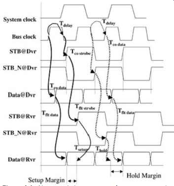
FIG. 9: Alternate timing sequence for a source synchronous bus.
3. ALTERNATIVE BUS SIGNALING TECHNIQUES
As speeds increase, source synchronous timing is getting ever more difficult to implement. It gets significantly more difficult to control skew as frequencies increase. Nonideal effects such as simultaneous switching noise, nonideal return paths, intersymbol interference, and crosstalk increase skew dramatically. Furthermore, any sockets or connectors also introduce additional variables that could increase skew. As mentioned earlier, it is optimal to make the data and the strobe paths identical to each other so that they look the same at the receiver.
If the nets are identical (or at least close to identical), the timing and signal integrity differences will be minimal, subsequently, the skew will be minimized. One problem with conventional source synchronous timing techniques is that the strobe is sent out a significant amount of time after the data (usually several hundred pico-seconds to a few nano-seconds). During this time, noise from the core, power delivery or other parts of the system can be coupled onto the strobe, varying its timing and signal quality characteristics so that they differ from the data. This increases the skew significantly.
New bus signaling techniques that minimize the effect of skew are being developed continuously. Here are a few alternative techniques.
3.1. Incident Clocking
In the technique of incident clocking, the data and strobe are sent out simultaneously instead of separated by a delay as in conventional source synchronous timings. This allows the data and the strobe to experience the same coupled noise and will subsequently be subjected to similar timing push-outs and signal integrity distortions. The result will be a decrease in the skew at the receiver and subsequently an increase in the maximum speed. But if the data and strobe are sent out simultaneously, how are the setup- and hold-time requirements of the receiver satisfied? The only obvious way is to delay the strobe on the silicon at the receiver; however, this partially defeats the original intent of incident strobing because noise can be coupled into the strobe in the receiving circuitry during the strobe delay. Theoretically, however, the coupled noise should be significantly smaller than in conventional source synchronous architecture.
3.2. Embedded Clock
Another promising alternative to source synchronous timing is to embed the clock into the data signal by borrowing techniques from the communication industry. This technique would eliminate the need for a separate strobe. In this technique, a PLL constructs a clock from the data patterns themselves. However, since the PLL requires some minimum data switching in order to construct a clock, there is some overhead in maintaining sufficient data signals. For example, if the data to be transmitted consist of a long string of 0's, the algorithm must send periodic 1's to keep the PLLs in the driver and receiver in phase. Although this technique sounds promising, it is estimated that the algorithm would require approximately a 20% overhead; that is, for every 8 bits of data transmitted, two clocks are transmitted.