AMAZON multi-meters discounts AMAZON oscilloscope discounts
The three subjects of this Section--nonideal return paths, simultaneous switching noise, and local power delivery--are very closely related. In fact, sometimes the effects are indistinguishable in a laboratory setting. In the past, these effects were often ignored during the design process, only to be discovered and patched after the initial systems were built. As speeds increase, however, the patches become ineffective, and these effects can dominate the performance. The reader should pay close attention to this Section because it’s probably one of the most difficult subjects to understand. Furthermore, careful attention to the issues presented in this Section is essential for any high-speed design. Often, designers hope that these issues won’t be of consequence and subsequently ignore them. However, hope is a precious commodity. It’s better to be prepared.
NONIDEAL CURRENT RETURN PATHS
So far, this guide has covered virtually everything necessary to model the signal path as it propagates from the driving circuitry to the receiver through packages, sockets, connectors, motherboard traces, vias, and bends. Now it’s time to focus on what is often considered the most difficult concept of high-speed design, nonideal return paths. Many of the effects detailed in this section are very difficult or impossible to model using conventional circuit simulators. Often, full-wave simulators are required to capture the full effects. Subsequently, in this section we focus less on specific modeling techniques and more on the general impact and physical mechanisms of the return current path that affect the system. As a general rule, great care should be taken to ensure that nonideal current return paths are minimized.
Path of Least Inductance
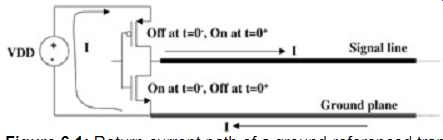
FIG. 1: Return current path of a ground-referenced transmission line
driven by a CMOS buffer.
As was discussed in Section 2, the signal propagates between the signal trace and the reference plane. It does not merely propagate on the signal line. Subsequently, the physical characteristics of the reference plane are just as important as that of the signal trace. A very common mistake, even for experienced designers, is to focus on providing a very clean and controlled signal trace with no thought whatsoever of how the current is going to return. Remember that any current injected into a system must return to the source. It will do so through the path of least impedance, which in most cases means the path of least inductance. FIG. 1 depicts a CMOS output buffer driving a microstrip line. The currents shown represent the instantaneous currents that occur when the driver switches from a low state to a high state. Just prior to the transaction (time = 0- ), the line is grounded via the NMOS. Immediately after the transaction (time = 0+ ), the buffer switches to a high state and current flows into the line until it’s charged up to Vdd. As the current propagates down the line, a mirror current is induced on the reference plane, which flows in the opposite direction. To complete the loop, the current must find the path of least inductance, which in this case is the voltage supply Vdd.
When a discontinuity exists in the return path, the area of the loop increases because the current must flow around the discontinuity. An increase in the current loop area leads to an increase in inductance, which degrades the signal integrity. Subsequently, the most fundamental effect of a discontinuity in the return path is an effective increase in series inductance. The magnitude of the inductance depends on the distance the current must diverge.
Signals Traversing a Ground Gap
To demonstrate the effect of a long-return current path, refer to FIG. 2, which depicts a microstrip line traversing a gap in its ground reference plane. This is a convenient ground return path discontinuity to begin with because it’s a simple structure, the return current path is well understood, and its trends can be applied to more general structures. As the signal current travels down the line, the return current is induced onto the ground plane. However, when the signal reaches the gap, a small portion of the ground current propagates across the gap via the gap capacitance, and the other portion is forced to travel around the gap. If there were no gap capacitance and the gap was infinitely long, the line crossing the gap would appear to behave as an open circuit, due to the impedance increase from the simultaneous increase in series inductance and decrease in capacitance to ground.
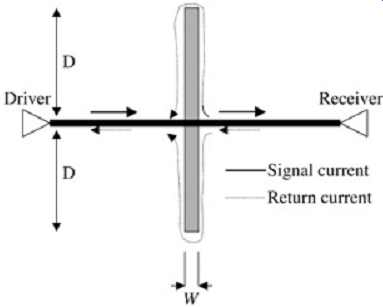
FIG. 2: Driving and return currents when a signal passes over a gap
in the ground plane.
FIG. 3 shows some general receiver wave-shape characteristics when a signal line crosses a gap, as in FIG. 2. If the distance of the current return path (2D in FIG. 2) is small compared to the edge rate, the gap will simply look like a series inductance in the middle of the transmission line. The extra inductance will filter out some of the high frequency components of the signal and degrade the edge rate and round the corners. This is shown in the first graph of FIG. 3a. When the electrical length of the return path, however, becomes longer than the rise or fall times, a ledge will appear in the waveform.
The length of the ledge (in time) will depend on the distance the return current must travel around the discontinuity, as shown in FIG. 3a. Since the width of the gap will govern the bridging capacitance, and thus the portion of current shunted across the gap [I = Cgap(dV / dt)], the height of the ledge will depend on the gap width, as shown in FIG. 3b. The larger the gap width, the less the capacitive coupling and the lower the height of the ledge.
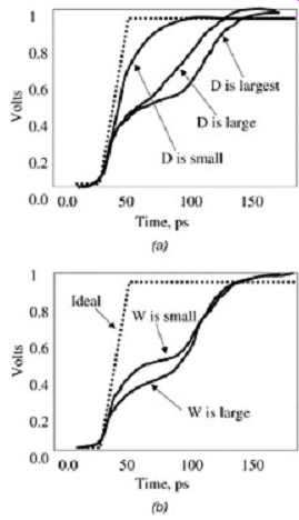
FIG. 3: Signal integrity as a function of ground gap dimensions: (a)
signal integrity as a function of return path divergence length; (b) signal
integrity as a function of gap width.
Another effect of this specific nonideal return path is a very high coupling coefficient between traces traversing the same gap. The coupling mechanism is the gap itself. Energy is coupled into the slot and it propagates down to the other line via the slotline mode. A slotline is a transmission line in which the fields establish themselves between the conductors on both sides of the slot. The top portion of FIG. 4 is an example of coupling through a gap in the reference plane. Measurements will show significant coupling to other lines traversing the same gap even when the line is well over an inch away! In this case, nearly 15% of the total energy driven into the driver line is coupled to the adjacent line, 1.4 in. away.
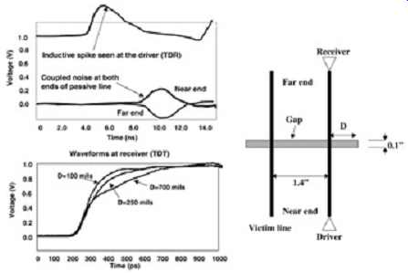
FIG. 4: TDR/TDT response and coupled noise of a pair of lines passing
over a slot in the reference plane.
FIG. 4 also shows the TDR response of a line traversing a gap. Notice that from the driver's point of view, the return path discontinuity looks like a series inductance. Finally, the bottom portion of FIG. 4 shows the response at the end of the line. Notice that when the return path distance (D) is small, the edge rate is decayed due to the inductive filtering effect.
When D become larger, a ledge begins to form.
Modeling a Signal Traversing a Gap.
For small current diversion paths (i.e., small gap lengths), the discontinuity can be modeled as a series inductor.
Equation (1) and FIG. 2 can be used to determine a first-order approximation of the inductance. To determine a more accurate model, a three dimensional simulator or measurements from the laboratory should be used.
(1)
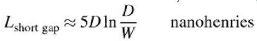
...where L is the inductance, D the current divergence length, and W the gap width. Assuming that the discontinuity appears in the middle of a long net, the degradation of an input step can be approximated using the equation:
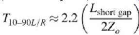
(2)
The following equation can be used to estimate the rise or fall time after it has passed over the gap, where Tinput is the rise or fall time (10 to 90%) of the signal before the gap and Tgap is the rise or fall time seen after the gap.
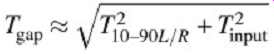
(3)
If the gap is electrically close to a receiver capacitance, three time constants should be used to estimate the 10 to 90% edge rate in place of equation (2).
It should be noted that routing more than one line over a gap in the reference plane should never be done on high-speed signals, and the reference plane under the signals should remain continuous whenever possible. The reason the short gap equations were presented is because it’s sometimes necessary to route over package degassing holes or via antipads in some designs. The formulas above can help the designer estimate the effects. If traversing a ground gap is unavoidable, the effect can be minimized by placing decoupling capacitors on both sides of the signal line to provide an ac short across the gap. This will effectively shorten the gap length (D) by providing an ac short across the gap. However, it’s usually impossible to place a capacitor between each line on a bus.
Examination of a signal line traversing a gap in the ground plane leads to some general conclusions about nonideal return paths.
RULES OF THUMB: Nonideal Return Paths
-- A nonideal return path will appear as an inductive discontinuity .
-- A nonideal return path will slow the edge rate by filtering out high-frequency components.
-- If the current divergence path is long enough, a nonideal return path will cause signal integrity problems at the receiver.
-- Nonideal return paths will increase current loop area and subsequently exacerbate EMI.
-- Nonideal return paths may significantly increase the coupling coefficient between signals.
Signals That Change Reference Planes

FIG. 5: Current paths when a signal changes a reference plane.
Another nonideal return path that is very often overlooked is a signal changing reference planes. For example, FIG. 5 shows a CMOS output driving a transmission line. The transmission line is initially referenced to the power plane (Vdd). The transient return current, Im, is induced on the power reference plane and flows directly beneath the signal line for a distance of X. The return current is shown as a negative value flowing in the same direction as the signal current. As the signal transitions to a ground plane reference, the return current cannot flow directly beneath the signal line. Subsequently, just as with the reference plane gap shown in FIG. 2, the return current will flow through the path of least inductance so that it can complete the loop. In this case, however, instead of flowing around a gap in the reference plane, it will find the easiest path between planes. In this particular case, the easiest path is the Vdd power supply. It’s easy to draw parallels between a signal switching reference planes and a signal traversing a gap. Obviously, since the current loop is increased, excess series inductance will be induced. This will degrade the edges and will cause a signal integrity problem in the signal waveform if the return path is long enough.
Additionally, this particular example assumes that the return path is through an ideal voltage supply. In reality, the return path will be inductive and will probably be through a decoupling capacitor, not the power supply. Changing reference planes should always be avoided for high-speed signals. If it’s absolutely necessary, however, the decoupling capacitance should be maximized in the area near the layer change. This will minimize the return current divergence path.
Signals Referenced to a Power or a Ground Plane
This type of return path discontinuity is almost never accounted for in design and can lead to severe problems. Initially, let's examine what happens to the return currents when a CMOS output is driving a ground-referenced microstrip transmission line as depicted in FIG. 6. If the system is at steady state low and switches high, the return current in the ground plane must flow through the capacitor to complete the loop. The capacitor represents the local decoupling capacitance, which will usually be at or near the die. If this capacitance is not large enough, or there is significant inductance in the path, or if the closest decoupling capacitor is far away, the signal integrity will be affected adversely.
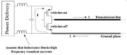
FIG. 6: Return current for a CMOS buffer driving a ground-referenced
microstrip line.
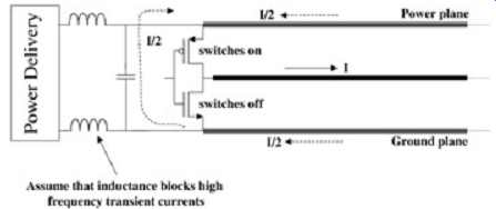
FIG. 7: Return current for a CMOS buffer driving a dual-referenced (ground
and power) stripline.
When designing a system, the engineer should examine the return currents very carefully and ideally should choose a stackup that will minimize transient return current through the decoupling capacitor. For example, since a typical CMOS output buffer pulls an equal amount of current from power and ground, the optimal solution is to route the signal in a symmetric stripline that is referenced to both power and ground. If such a circuit is referenced to only a power or a ground plane, the return current through the decoupling capacitance will be equal to the mirror current in the reference plane as shown in FIG. 6. If the line is symmetrically referenced to power and ground, as shown in FIG. 7, the maximum current flowing through the decoupling will be approximately 1. FIG. 8 shows a GTL buffer driving a microstrip line that is referenced to the ground plane.
The capacitance C represents the local decoupling capacitance at the I/O cell of the die. The network to the left of the driver represents a simplified power delivery network that is discussed in Sect. 2.
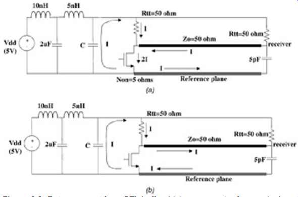
FIG. 8: Return current for a GTL buffer driving a ground-referenced
microstrip line: (a) pull-down (NMOS switched on); (b) pull-up (NMOS switched
off).
In this example it’s assumed that the inductance of the power supply blocks the high frequency ac signals, which forces the return current to flow through the capacitance. The figure of merit is the amount of current forced through the decoupling network. It’s optimal to choose the reference plane so that the minimum amount of current is forced through the decoupling capacitors.
Example 1: Calculation of Return Current for a GTL Bus High-to-Low Transition.
Refer to FIG. 8. Assume that impedance of the NMOS can be approximated by a 5-? resistor and the bus is just switching from steady state high to low. When the circuit pulls the net low, the voltage across the NMOS can easily be calculated.
Therefore, for the pull-down condition in FIG. 8, the current forced though the decoupling capacitance is 83 mA. This is deduced by summing currents at the NMOS-transmission line junction and at the NMOS-ground plane junction.
FIG. 9 shows the return currents for a power-plane-referenced microstrip line. Notice that no current is forced through the decoupling capacitance for the pull-up transition, but twice the current is forced through the decoupling capacitor for the pull-down transition.
Subsequently, it can easily be concluded that it’s preferable to route a GTL bus over ground planes unless it can be proven that the local decoupling is adequate to pass the return currents without distorting the signal .
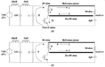
FIG. 9: Return current for a GTL buffer driving a power referenced microstrip
line: (a) pull-down; (b) pull-up.
FIG. 10 are some simulations showing the difference between ground-and power referenced buses for the circuits shown in Figures 8 and 9. Notice that the ground-plane referenced microstrip exhibits much cleaner signal integrity than the power-plane-referenced signal. Also note that the signal integrity for both cases improves significantly when the local decoupling capacitance C is increased so that the capacitor looks like a short to the transient return currents.
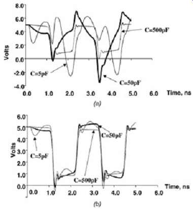
FIG. 10: Signal integrity as a function of local decoupling capacitance:
(a) power plane-referenced microstrip; (b) ground-plane-referenced microstrip.
(Circuits simulated are shown in Figures 8 and 9.)
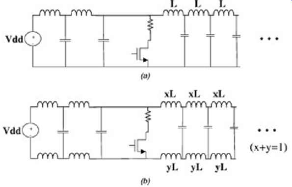
FIG. 11: (a) Unbalanced versus (b) balanced transmission line models.
Since it’s important to model all current return paths explicitly through the power delivery system, it’s necessary to use only one ground in the system simulation and explicitly force all current to flow as they would in the real system. There are two ways to do this. The easiest way is to construct a traditional LRC model as depicted in FIG. 11a and tie all the grounds to a common point so that the current is forced to flow through the power delivery system. If a specialized transmission line model included in a simulator is used, however, the ground-referenced points cannot necessarily be tied to anything other than perfect ground, because it might cause convergence problems, depending on the model. The alternative, which is technically more correct, is to use a balanced transmission line model instead of the traditional unbalanced model. A balanced model has inductance in the top and bottom portions so that an explicit ground return path can be modeled. Unfortunately, this typically takes a very long time to converge during simulation. Convergence can be expedited, however, if resistive elements are included in the simulation. FIG. 11 shows the difference between a balanced and an unbalanced return path model. In the balanced model, the inductance (L) is split up between the signal layer and the ground layer. The amount of inductance in each layer depends on the current distribution. Since this is difficult to calculate without a three dimensional simulator, it’s usually a valid approximation to include 80% of the inductance in the signal layer and 20% of the inductance in the plane layer. In most designs, simulations are performed with the unbalanced topology.
It should be noted that accurate modeling of this return path phenomena depends on the power delivery network. Subsequently, it’s prudent to read the subject of power delivery (Sect. 2) prior to creating any models .
Other Nonideal Return Path Scenarios
There are significantly more nonideal return path scenarios than can be covered in this guide.
However, the discussion so far should have provided a basic understanding of the effects.
Here is a brief list of some return path discontinuities not discussed .
-- Meshed power/ground planes
-- Signals passing over or near via antipads
-- Transitions from a dual-referenced (power and ground) stripline to a single-referenced (just power or ground) microstrip or offset stripline
-- Transitions from a package to a board
Differential Signals
When a return path discontinuity exists, the effect can be minimized through the use of differential signaling (odd-mode propagation). To explain why, refer to the odd-mode electric field shown in FIG. 10. Notice that the electric fields always intersect the ground planes at 90° angles. Also notice that it’s possible to draw a line through the electric field patterns between the conductors such that the electric field lines are always perpendicular to it (only in odd mode). This illustrates the fact that a virtual ground exists between the two conductors in an odd-mode pattern. When an odd-mode signal is propagating over a nonideal return path, the virtual ground provides an alternative reference to the signals so that a return path that is not perfect affects the signal quality to a lesser degree. Furthermore, the current through the decoupling capacitance will be minimized because when one driver is pulling current out of a supply, the complimentary driver is dumping current into the same plane.
Subsequently, the currents through the decoupling capacitors will cancel. Differential signaling will dramatically improve the signal quality when nonideal effects from return paths, connectors or packages are present. Unfortunately, practical limitations such as package pin count, board real estate and receiver circuit complexity often negate the advantages gained from differential signaling.
LOCAL POWER DELIVERY NETWORKS
Power delivery will initially be discussed only as it pertains to the performance of the I/O buffers and the interconnects on the bus. The reader should note that although the analysis of local power delivery networks share much in common with system-level power delivery, the focus is different. The focus is supplying the required high-frequency current to the I/O buffers.
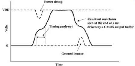
FIG. 12: Telltale sign of a power delivery problem.
Consider the LC ladder to the left of the GTL output buffer depicted in FIG. 8. This is a very simplified network intended to represent the power supply as seen through the eyes of the output buffer. The ideal voltage supply represents the voltage at the system voltage regulator module (VRM), which provides a stable dc voltage to the system. The first 10-nH inductor crudely represents the inductive path between the VRM and the first bulk decoupling capacitor, whose value is 2 µF. The 5-nH inductor represents the path inductance between the bulk decoupling capacitor and the I/O cell on the die. As mentioned above, the capacitor C represents the local decoupling on the die at the I/O cell. As mentioned earlier, this is only a very crude representation of a power delivery system; however, it’s adequate to achieve first-order approximations and is excellent for instructional purposes. A full model would require extraction from a three-dimensional simulator (or measurements) and would be implemented in a simulator with a mesh of inductors that resembles a bedspring. Alternatively, full-wave simulators that use the finite-difference time domain (FDTD)-based algorithms can be used to optimize the local power delivery system.
The FDTD simulator approach will yield more accurate responses of the board and package interactions; however, it’s usually very difficult or impossible to model the active circuitry correctly in such simulators. To approximate the first-order effects, however, it’s adequate to represent the power delivery system in the simplified manner discussed here and to ensure that the decoupling capacitance is adequate so that the local power delivery system won’t affect the signal integrity.
The problem is that when the output buffer switches, it quickly tries to draw current from the VRM. The series inductance to the VRM will limit the current that can be supplied during the switching time. If the inductance is large enough, it will essentially isolate the output buffer from the power supply when current is drawn at a fast rate. If the inductance is high enough, it essentially looks like an open circuit during fast transitions and will block the flow of current.
Subsequently, the power seen at the I/O cell will droop because the local power delivery system cannot supply the required current. This effect has many names, including power droop, ground bounce, and rail collapse. Whatever it may be called, it can devastate the signal integrity if not accounted for properly.
Ideally, the elimination, or the significant reduction of the series inductance, will solve the problem of rail collapse. However, reality eliminates the ideal solution because it’s impossible to place a VRM in close proximity to every I/O cell. The next best thing is to place decoupling capacitors as close as possible to the component. The decoupling capacitors will be charged up by the VRM and will act like local batteries or mini power supplies to the I/O cell. If the decoupling capacitance is large enough and the series inductance to the decoupling capacitors is small, they will supply the necessary current during the transition and preserve the signal integrity. FIG. 10 depicts the signal integrity as a function of local I/O capacitance. The capacitance C represents the local capacitance at the I/O cell as depicted in Figures 8 and 9. Notice that the signal integrity gets progressively better as the local capacitance is increased .
Another effect of power droop is a timing push-out in the form of a ledge, as shown in FIG. 12. This effect is quite common, especially in CMOS output drivers. As the CMOS gate pulls up, it will pull current out of the power supply at a fast rate. If the series inductance to the supply is large enough, it will limit the current and cause a decrease in the voltage seen at the drain of the PMOS. Subsequently, the voltage at the output will decrease, causing a ledge in the rising edge of the waveform. Similar effects occur when the NMOS is pulling the net to ground and attempting to sink current. A waveform of this shape ( FIG. 12) seen in the laboratory is a telltale sign that the decoupling of the power supply is inadequate. Be certain, however, that the waveform is on the receiving end of a net and not at the driver. A similar waveform is expected at the driver of a transmission line due to the initial voltage divider between the output impedance and the transmission line impedance (e.g., see FIG. 14). A ledge can also be caused by other effects such as a long stub (e.g., FIG. 15). Don’t get these phenomena confused.
Fundamentally, this leaves us with two critical components of the local power delivery system as it pertains to the output buffers and signal integrity: the value of the nearest decoupling capacitance and the inductive path to that capacitance. Often, the major decoupling mechanism, depicted in Figures 8 through 10, is the natural on-die capacitance. Other times, it’s the closest decoupling capacitors on the board. At any rate, it’s essential to place the capacitance as close as possible to the component. Sometimes this is achieved by designing a chip package with an area underneath that is devoid of pins for the placement of decoupling capacitors directly beneath the die. These are sometimes referred to as land-side capacitors and can dramatically improve the local power delivery system.
Another consideration when designing a system is power delivery resonance. This occurs when the decoupling capacitance and the series inductance resonates like a simple tank circuit. (More information on decoupling resonance is provided in Section 10) This will be as shown in FIG. 10 when the capacitance at the die is 5 pF. It’s much more evident in the power-plane-referenced example; however, it’s definitely noticeable in the ground plane-referenced circuit. The resonance occurs between the 5-pF capacitance at the die and the 5-nH series inductance to the first bulk decoupling capacitance. This resonance of a parallel L and C forms a high impedance pole at which it will be very difficult to draw power.
In this case the resonance is calculated as:
It should be noted that the resonance might be calculated differently in other systems. Only careful examination of the power delivery system will yield the proper resonance equation. It’s vital that the resonance of the power supply network be considered during design so that it won’t adversely affect signal integrity.
Determining the Local Decoupling Requirements for High Speed I/O
Ideally, it’s optimal to design enough on-die capacitance into the silicon to provide adequate power delivery to the output buffer. However, it’s not always possible to do so. When the on die capacitance is not sufficient, it’s necessary to compensate with external capacitors. The minimum on-die capacitance that is required to eliminate signal integrity problems can be approximated using the following process.
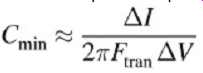
__ Determine the maximum amount of noise your logic can tolerate due to local power supply fluctuations. Remember, power droop is only one component of the total noise, so de-rate this number accordingly. We will call this number ?V.
__ Determine the maximum amount of return current that will be forced to flow through the decoupling capacitance. We will call this number ?I .
__ Subsequently, ?V/?I is the maximum impedance that the path through the local on die decoupling can tolerate.
__ Approximate the transient frequency the on-die capacitance must pass. There are many ways to do this. One method is to use the equation...
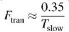
... which is derived in Section C, where Tslow is the slowest edge rate the driver will produce. It’s important to choose the slowest edge rate because a capacitor will pass high frequencies. If the fastest edge rate is used in this calculation, signal integrity problems may arise for components with slower edge rates because the capacitor won’t pass the lower-frequency components of the slower edge rate. Alternatively, the engineer may choose use the fundamental maximum bus frequency or Fourier analysis methods to determine the frequencies that must be decoupled by the capacitor.
__ The minimum on-die capacitance per I/O cell is calculated as...
If the on-die capacitance per I/O cell is smaller than Cmin, the board or land-side decoupling capacitance must compensate. The main problem, as discussed previously, is the series inductance to the decoupling capacitor. This inductance must be kept small enough so that it won't limit the current to the nearest capacitor. Unfortunately, since it will be almost impossible to provide a board-level decoupling capacitor for each I/O cell, each capacitor must provide the decoupling for several output buffers. Furthermore, the inductive path to that capacitor is also shared. To determine the requirements of the closest board-level decoupling capacitors, both the inductive path and the capacitance value must be investigated. The inductance must be small enough and the capacitance must be large enough. The following procedure approximates the requirements assuming the on-die capacitance is not adequate.
__ Again, determine the maximum amount of noise your logic can tolerate due to local power supply fluctuations. We will call this number ?V.
__ Determine the maximum amount of return current that will be forced to flow through the inductive path to the decoupling capacitance. One way to approximate this is to determine the total number of I/O cells per board-level decoupling capacitors. Since the return current of each I/O will be forced to flow through the capacitor, the sum will be ?Isum. For example, if the ratio of I/O cells to decoupling capacitors is 3 : 1, the return current of three output buffers will be forced the flow through each capacitor.
__ Determine the transient frequency of the edge as in step 4 of the earlier list in this section. It’s important to note, however, that the fastest rise/fall time should be used because an inductor will pass low frequencies.
__ Calculate the maximum tolerable series inductance to the cap as ...
__ Calculate the minimum value of the decoupling capacitance with equation (6) using the value ?Isum in place of ?I. Remember, for the minimum capacitance value, use the slowest rise or fall time. This will ensure the capacitance is large enough to pass all frequencies.
The value of Lmax will obviously depend on the distance between the I/O cells and the decoupling capacitors. It will also depend on the package, socket, via, and capacitor lead inductance. The package, via, and socket inductance can be approximated using the techniques discussed in Section 5. The series inductance of the capacitor itself can either be measured or provided by the manufacturer. The determination of the plane inductance will require a three-dimensional simulator or a measurement to determine accurately; however, it can be approximated to the first order by using either a two-dimensional simulator or plane inductance equations. It should be noted that the total inductance contributed by sockets, chip packages, bond wires, vias, and so on, is typically much higher than the plane inductance .
To crudely approximate the plane inductance between the package power pin and the nearest decoupling capacitor, the following steps can be followed .
__ Determine the ratio of local decoupling capacitors to output buffers. This will provide an estimate of the number of signals decoupled by each capacitor.
__ Approximate the area on the PCB power plane where the current will flow. This may prove to be very difficult without a three-dimensional simulator. The area is important because it will be used to calculate the plane inductance of the path between the power pin and the decoupling capacitor. If sound engineering judgment is used, the area may be approximated within an order of magnitude. Since the current will always travel through the path of least inductance, a straight line can usually be assumed.
The problem is estimating how much the current will spread out. One way of roughly estimating the spread is shown in FIG. 13. In FIG. 13, the ratio of power pins to capacitors is 2 : 1. Subsequently, the approximate area where the current will flow can be approximated by the triangle shown.
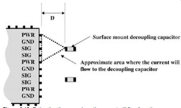
FIG. 13: Estimating the area where the current will flow from the component
to the decoupling capacitor.
__ Determine the plane inductance between the package power pin and the nearest decoupling capacitor. This can be approximated by constructing a rectangle with the same area as the triangle shown in FIG. 13 and simulating it in a two-dimensional solver as a wide transmission line with a length of D. Alternatively, the following equation can be used:
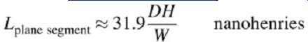
... where D is the length of the plane segment in inches, H the separation between the power and ground planes (in inches), and W the width in inches. This should provide an estimate that is accurate to at least one order of magnitude. If a more accurate number is required, a three-dimensional simulator or laboratory measurements are required.
FIG. 14 shows an equivalent circuit of a GTL bus where three output buffers are sharing one board level decoupling capacitor. A full model would include the crosstalk in the package and socket.
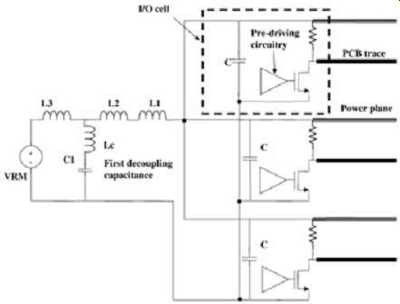
FIG. 14: Equivalent circuit of three GTL drivers and a component-level
power delivery system. C, on-die I/O cell capacitance; C1, first-level
decoupling capacitor; L1, package and socket equivalent inductance; L2,
PCB plane inductance from package power pin to decoupling capacitor; L3,
inductance to the VRM; Lc, lead inductance of the capacitor.
System-Level Power Delivery
The subject of system-level power delivery is discussed only briefly in this guide. The subject is also discussed in Section 10. Typically for interconnect design, the power delivery required for analysis of the bus performance is at the component level, as discussed in Sect. 2. This discussion is intended only to provide the designer with a fundamental understanding of system-level power delivery.
A system-level power delivery network is designed to provide stable and uniform voltages for all devices. It’s very important that the system power level be kept uniform across the board because fluctuations in reference and/or supply voltages will significantly affect the timing and signal integrity of individual components. Such variations can lead to component-to component skews that can consume precious timing budgets. These devices usually require a low-impedance voltage source that is able to supply the necessary current when the logic gates switch. If the components were connected directly to the power supply or the VRM, there would be no need to worry about system-wide power delivery. Unfortunately, the power supply of the system is distributed via a network of inductive planes and wires. Subsequently, when numerous gates switch simultaneously on several different components, the inductance and resistance of the planes and wires will exhibit high-impedance characteristics and may limit the amount of current that is available instantaneously. The purpose of system-level power delivery is to provide and adequate supply to satisfy all current demand of the system-level components.
There are essentially two levels of power delivery that must be accounted for in a digital system, the low frequency and the high frequency. The high frequency is required at the component level, which was described previously in this Section with a focus on the I/O circuitry. However, the core logic of a device also requires high-frequency power delivery.
Basically, the high-frequency component of the power delivery system must supply the instantaneous current demanded at the part. As described above, this is achieved by placing capacitors as close as possible to the component and maximizing the on-die capacitance.
Subsequently, the capacitors will act like local batteries to provide the necessary current.
These capacitors need to be large enough so that an adequate amount of charge can be stored in order to supply the required current. The problem is that once the capacitors are depleted of charge, they can no longer provide the current until they are charged up again. If there is a large inductive path between the high-frequency capacitors at the component and the voltage supply, they won’t be charged up in time to provide current when it’s required.
The solution is to add more decoupling capacitance between the voltage supply (VRM) and the component. If done correctly, this will supply a charge reservoir that will recharge the component-level capacitors. This second tier of decoupling capacitance will usually be much larger than the component or first-tier capacitors. The bandwidth requirements of the decoupling network will decrease as the capacitors move away from the component. They don't need to support the full di/dt value of the logic; they only have to support a bandwidth high enough to recharge the first-tier capacitors before they are required to supply current to the local component. Sometimes it’s required to have several tiers of decoupling capacitors between a system power supply and the components to guarantee a stable and uniform voltage reference across the board. As the capacitors move away from the component, the frequencies they must support become lower.
Choosing a Decoupling Capacitor
Capacitors are not perfect. Every discrete capacitor has a finite lead inductance associated with it that will cause the impedance of the decoupling capacitor to increase when the frequency gets high enough. They also have a finite resistive loss that will decrease the effectiveness of the capacitor [called effective series resistance (ESR)]. Furthermore, every capacitor is temperature sensitive, which may cause its dielectric properties to vary and cause wide swings in capacitance. The capacitance of a capacitor may also change slowly over time due to aging of the dielectric material. Finally, they will explode if subjected to excessive voltage. When choosing a bypass capacitor, it’s important to comprehend each of these imperfections. The effect of the inductance and ESR can be calculated. Only the manufacturer can provide detailed information on temperature sensitivity, aging, and maximum voltage.
The figure of merit for a decoupling capacitor is its equivalent ac impedance. This is estimated using a root-mean-square approach including the impedance of the resistance, inductance, and capacitance:
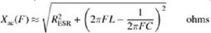
...where RESR is the series resistance of the capacitor, Xac the equivalent ac impedance of the capacitor, and L the sum of the lead, package, and connector inductance of the discrete capacitor.
FIG. 15 is a frequency response of a realistic capacitor. The impedance of the inductance, capacitance, and resistance is plotted versus frequency on a log-log scale so that it can be analyzed easily. The results of equation (9) are also plotted. Notice the bandpass characteristics. At low frequencies, the capacitor behaves like a capacitor. When the frequency gets high enough, the inductive portion takes over and the impedance increases with frequency.
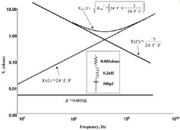
FIG. 15: Impedance versus frequency for a discrete bypass capacitor.
The impedance of the capacitor will depend largely on the frequency content of the digital signal. Therefore, it’s important to choose this frequency correctly. Unfortunately, it’s not very straightforward in a digital system because the signals contain multiple frequency components. There are several ways to choose the maximum frequency that the bypass capacitor must pass. Some engineers simply choose the maximum frequency to be the fifth harmonic of the fundamental. For example, if a bus is running at a speed of 500 MHz, its fifth harmonic is 2500 MHz (see Section C). Usually, the rising and falling edges of a digital signal produce the highest-frequency component. Subsequently, the following equation (also explained in Section C) can be used to approximate the highest frequency that the bypass capacitor must pass: (10)
If the lead inductance or the ESR of the capacitor is too high, either choose a different one or place several capacitors in parallel to lower the effective inductance and resistance.
Frequency Response of a Power Delivery System
Of course, the frequency response of the entire power delivery network is what is important.
The system power supply must look low impedance at all frequencies of interest. FIG. 16 shows how the ac impedance will vary as a function of frequency for a simple power delivery system. Bode plot techniques were used to estimate the impedance as a function of frequency for the power delivery system. Note that the power delivery inductance, Lpwr, plays a significant role in the frequency response. In this analysis, the effect of the series resistance (ESR) was ignored. Another effect that is ignored in this analysis is the possibility of resonant poles that can significantly increase the impedance of the power delivery system.
These resonant poles are covered briefly in Section 10.
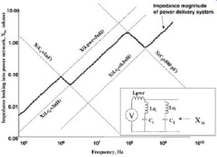
FIG. 16: Frequency response of a simple power delivery system.
SSO/SSN
Simultaneous switching output noise (SSO), which is sometimes referred to as simultaneous switching noise (SSN) or delta-I noise, is inductive noise caused by several outputs switching at the same time. For example, a signal switching by itself may have perfect signal integrity. However, when all the signals in a bus are switching simultaneously, noise generated from the other signals can corrupt the signal quality of the target net.
SSN is typically very difficult to quantify because it depends heavily on the physical geometry of the system. The basic mechanism, however, is the familiar equation:
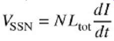
...where VSSN is the simultaneous switching noise, N the number of drivers switching, Ltot the equivalent inductance in which current must pass, and I the current per driver. When a large number of signals switch at the same time, the power supply must deliver enough current to satisfy the sudden demand. Since the current must pass through an inductance, Ltot, a noise of VSSN will be introduced onto the power supply, which in turn will manifest itself at the driver output.
SSN can occur at both the chip level and the board level. At the chip level, the power supply is not perfect. Any sudden demand for current must be supplied by the board-level power though the inductive chip package and lead frame (or whatever the connecting mechanism happens to be). On the board level, sudden current demands must be supplied through inductive connectors. As discussed in Section 5, any current flowing through a connector must be supplied and return through the power and ground pins, which will induce noise into the system. Furthermore, as discussed in Sect. 1, a nonideal return path will also cause an effective increase in the series inductance in the vicinity of the discontinuity. Furthermore, if the return path discontinuity forces the return current from several outputs to flow through a small area, SSN will be even more exacerbated.
Many of the mechanisms that contribute to SSN were discussed above and 5.
The area that needs further explanation is the chip/package-level SSN.
To explain how SSN will affect signals on the chip, refer to FIG. 17.
The inductors represent the equivalent inductance seen at the power connections
and the output of each I/O. As drivers 1, 3, and 4 switch simultaneously,
several inductive noises will be generated. First, as the transient current
flows through the power supply inductors, di/dt noise will be generated.
This noise will be coupled to the power connections of quiet nets. It’s
possible for the power supply to get so noisy that it causes core logic
to flip state. In another failing case, the input of a strobe or a clock
receives enough noise that exceeds its threshold voltage, causing a false
trigger. SSN will also distort the signal integrity, which can cause
gate delays, which will sometimes be manifested as shown in FIG. 12.
FIG. 17: Simultaneous switching noise mechanisms.
SSN can be a very elusive noise to characterize. There are not many methods for quick approximations to get an easy assessment of SSN. Only careful examination of your package and power delivery system and detailed simulations can lead to a reasonable assessment of the magnitude of SSN. Even when attempts are made to characterize the noise accurately, it’s almost impossible to determine an exact answer because the variables are so numerous and the geometries that must be assessed are three-dimensional in nature and depend heavily on the individual chip package (or connector) and the pin-out. Because of the difficulty of this problem, it’s recommended that SSN be evaluated using both simulation and measurements. Subsequently, only general rules can be used to control this noise source.
FIG. 18 is a generic model that can be used to evaluate SSN in a CMOS bus. The capacitors, CI/O, are the inherent on-die capacitance for each I/O cell. Lchip represents any inductance seen on the chip between the CMOS gate and the power bus. Lpwr bus represents the inductance of the power distribution on the die and package. Lgnd bus represents the inductance of the ground distribution on the die and on the package. and Lgnd pin represent the inductance of the power and ground pins on the package. LPCB plane represents the inductive path between the pin and the nearest decoupling capacitor. Lcap represents the series inductance of the decoupling capacitors, and represents the board-level decoupling capacitors. Finally, Lout represents the series inductance of the package seen at the I/O outputs. It should be noted that all mutual inductance values should be included in this model. Furthermore, the number of gates simulated should be equal to the number of gates that share the same power and ground pins.
FIG. 18: Model used to evaluate component level SSN/SSO for a CMOS-driven
bus. Connector SSN is simulated as described in Sect.
2.4. It’s important,
however, that the decoupling capacitors and the inductive path to the
capacitors be accounted for properly. If the general guidelines for connector
design described in Sect. 2.6 are adhered to, connector-related SSN will
be minimized. Nonideal return paths cause board-level SSN, which effectively
increases the series inductance of the net. Subsequently, the avoidance
of any nonideal return paths is critical. If a nonideal return path is
unavoidable, the board must be heavily decoupled in the area of the discontinuity
.
Minimizing SSN
The following steps may be taken to decrease the effects of SSN:
__ If possible, use differential output drivers and receivers for critical signals such as strobes and clocks. A differential output consists of a pair of signals that are always switching opposite in phase (odd mode). A differential receiver is simply a circuit that triggers at the crossing of two signals. This will eliminate common-mode noise and increase the signal quality dramatically. Differentially routed transmission lines will also be more immune to coupled noise and nonideal return paths because the odd mode sets up a virtual ground between the signals. It will also help even out the current drawn from the power supply.
__ Maximize the on-die capacitance. This will provide a charge reservoir that is not isolated by inductance. If the on-die capacitance is large enough, it will act like a local battery and compensate for a sudden demand in current.
__ Maximize the decoupling local to the component. Use land-side or die-side capacitors, if possible. Place the board capacitors as close as possible to the power and ground pins.
__ Assign I/O pins so there is minimum local bunching of output pins. Choose a pin-out that maximizes the coupling between signal and power/ground pins. Maximize the number of power and ground pins. Place power and ground pins adjacent to each other. Since current flows in opposite directions in power and ground pins, the total inductance will be reduced by the mutual inductance.
__ Reduce the edge rates. Be careful, though; this can be a double-edged sword. Slower edges are more susceptible to core noise. Laboratory measurements have shown that core noise can couple into the pre-driver circuitry during a rising or falling transition and cause jitter. The slower the transition, the more chance noise will be coupled onto the edge.
__ Provide separate power supplies for the core logic of a processor and the I/O. This will minimize the chance of SSN coupling into the core (or vice versa) and causing latches to switch state falsely.
7. Reduce the inductance as much as possible. Using fat power buses and short bond wires can do this.
8. When designing a connector, follow the guidelines in Sect. 2.6.
9. Minimize the inductance of the decoupling capacitors.
10. Avoid nonideal return paths like the plague.
11. Reference the PCB traces to the appropriate planes to minimize the current forced to flow through the decoupling capacitors, as in Sect. 1.4.