AMAZON multi-meters discounts AMAZON oscilloscope discounts
OVERVIEW
Digital design is entering a new realm. Bus speeds have increased to a point where high frequency phenomena that previously had second- or third-order effects on system performance have become first order. Many of these numerous high-speed issues have never needed to be considered in digital design of times past. Subsequently, modern high speed design not only requires the engineer to continuously break new ground on a technical level, but it also requires the engineer to account for significantly more variables.
Since the complexity of a design increases dramatically with the number of variables, new methodologies must be introduced to produce a robust design. The methodologies introduced in this Section show how to systematically reduce a problem with an otherwise intractable amount of variables to a solvable problem.
Many previous designs have used the route-simulate-route method. This old methodology requires the layout engineer to route the board prior to any simulation. The routed board is then extracted and simulated. When timing and/or signal integrity errors are encountered, the design engineer determines the necessary corrections, the layout is modified, and the loop begins all over again. The problem with the old methodology is that it takes a significant amount of time to converge and often does not provide a thorough understanding of the solution space. Even when a solution is determined, there may not be an understanding of why the solution worked. A more efficient method of design process would entail a structured procedure to ensure that all variables are accounted for in the pre-layout design. If this is done correctly, a working layout will be produced on the first pass and then the board extraction and simulation process is used only to double check the design.
The methodologies introduced in this section concentrate on efficiently producing high-speed bus designs for high-volume manufacturing purposes. Additionally, it outlines proven strategies that have been developed to handle the large number of variables that must be accounted for in these designs. Some of the highest-performance digital designs on the market today have been developed using these or a variation of the methodologies in this Section. Finally, in this section we introduce a specific design flow that allows the engineer to proceed from the initial specifications to a working bus design with minimal layout iteration.
This methodology will produce robust digital designs, improve time to market, and increase the efficiency of the designer.
1. TIMINGS
The only thing that really matters in a digital design is timings. Some engineers argue that cost is the primary factor; however, the cost assumption is built into most designs. If the design does not meet the specific cost model, it will not be profitable. If the timing equations presented in Section 8 are not solved with a positive margin, the system simply will not work.
Every concept in this book somehow relates to timings. Even though several Sections in this book have concentrated on such things as voltage ringback or signal integrity problems, they still relate to timings because signal integrity problems matter only when they affect timings (or destroy circuitry, which makes the timing equations unsolvable). This Section will help the reader relate all the high-speed issues discussed in this book back to the equations presented in Section 8.
The first step in designing a digital system is to roughly define the initial system timings. To do so, it is necessary to obtain first-order estimates from the silicon designers on the values of the maximum and minimum output skew, Tco, and setup and hold times for each component in the system. If the silicon components already exist, this information will usually be contained in the data sheet for the component. A spreadsheet should be used to implement the digital timing equations derived in Section 8 or the appropriate equations that are required for the particular design. The timing equations are solved assuming a certain amount of margin (presumably zero or a small amount of positive margin). Whatever is left over is allocated to the interconnect design. If there is insufficient margin left over to design the interconnects, either the silicon numbers need to be retargeted and redesigned, or the system speed should be decreased.
The maximum and minimum interconnect delays should initially be approximated for a common-clock design to estimate preliminary maximum and minimum length limits for the PCB traces and to ensure that they are realistic. If the maximum trace length, for example, is 0.15 in., it is a good bet that the board will not be routable. To do this, simply set the setup and hold margins to zero (using the equations in Section 8), solve for the trace delays, and translate the delays to inches using an average propagation speed in FR4 of 150 ps/in. for a microstrip or 170 ps/in. for a stripline. Of course, if the design is implemented on a substrate other than FR4, simply determine the correct propagation delay using equation (2.3) or (2.4) using an average value of the effective dielectric constant. In a source synchronous design, the setup and hold margins should be set to zero and the PCB skew times should be estimated. Again, the skews should be checked at this point to ensure that the design is achievable.
It should be noted that every single value in the spreadsheet is likely to change (unless the silicon components are off-the-shelf parts). The initial timings simply provide a starting point and define the initial design targets for the interconnect design. They also provide an initial analysis to determine whether or not the bus speed chosen is realistic. Typically, as the design progresses, the silicon and interconnect numbers will change based on laboratory testing and/or more detailed simulations.
1.1. Worst-Case Timing Spreadsheet
A spreadsheet is not always necessary for a design. If all the components are off the shelf, it may not be necessary to design with a spreadsheet because the worst-case component timings are fixed. However, if the components, such as a processor, chipset, or a memory component, is being developed simultaneously with the system, the spreadsheet is an extremely valuable tool. It allows the component design teams (i.e., the silicon designers) and the system design teams to coordinate with each other to produce a working system.
The spreadsheet is updated periodically and is used to track progress, set design targets, and perform timing trade-offs.
The worst-case spreadsheet calculates the timings, assuming that the unluckiest guy alive has built the system (i.e., all the manufacturing variables and the environmental conditions are chosen to deliver the worst possible performance). Statistically, a system with these characteristics may never be built, however, assuming that it will guarantee that the product will be reliable and robust over all process variations and environmental conditions.
Figures 1 and 2 are examples of worst-case timing spreadsheets for a source synchronous and a common-clock bus design, respectively. Notice that an extra term, Tguard, has been added into the equations. This represents the tester guard band, which is the accuracy to which the components can be tested in high volume. The tester guard band provides extra margin that is designed into the system to account for inaccuracies in silicon timing measurements which are always present in a high-volume tester. The spreadsheet is constructed so that each timing component can be tracked for each driver and each receiver.
The spreadsheets shown only depict a portion of the timings for the case when agent 1 is driving agent 2. The complete spreadsheets would depict the timings for each agent driving.
The target row refers to the initial estimations of each portion of the timing equation prior to simulation. The target numbers are based primarily on past design experience and "back of the envelope" calculations. The predicted row refers to the post-simulation numbers. These numbers are based on numerous simulations performed during the sensitivity analysis, which will be described later in this Section. The predicted Tva, Tvb, jitter, Tco, output skew, and setup/hold numbers are based off the silicon (I/O) designer's simulations and should include all the effects that are not "board centric." This means that the simulations should not include any variables under the control of the system designer, such as sockets, PCB, packaging, or board-level power delivery effects. The PCB skew and the flight time numbers constitute the majority of this book. These effects include all system-level effects, such as ISI, power delivery, losses, crosstalk, and any other applicable high-speed effect. Also note that the timings are taken from silicon pad at the driver to silicon pad at the receiver.
Subsequently, don't get confused by the terminology PCB skew, because that term necessarily includes any package, connector, or socket effects.
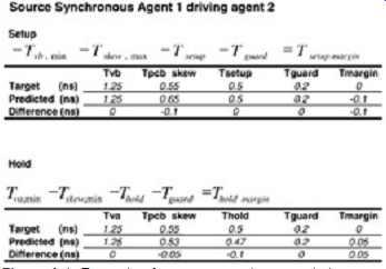
FIG. 1: Example of a source synchronous timing spreadsheet.
Also note that the signs on the clock and PCB skew terms should be observed
for the timing equations. For example, the common-clock equations indicate
that increasing the skew values will help the hold time because they are
positive in the equation. However, the reader should realize that the
signs are only a result of how the skew was defined, as in equations (5)
and (6). The skews were defined with the convention of data path, minus
clock path and the numbers entered into the spreadsheet should follow
the same convention. For example, if silicon simulations or measurements
indicate that the output skew between clkB and clkA (measured as TclkB
- TclkA) varies from -100 to +100 ps, the minimum value entered into the
common-clock hold equation is -100 ps, and the maximum value entered into
the setup equation is +100 ps. It is important to keep close track of
how the skews are measured to determine the proper setup and hold margins.
The proper calculation of skews is elaborated further in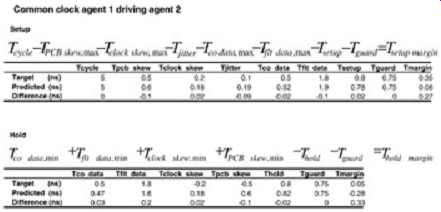 Section 9.2.
FIG. 2: Example of a common-clock timing spreadsheet.
1.2. Statistical Spreadsheets
The problem with using a spreadsheet based on the worst-case timings is that system speeds are getting so fast that it might be impossible to design a system that works, assuming that all components are worst case throughout all manufacturing processes.
Statistically, the conditions of the worst-case timing spreadsheet may happen only once in a million or once in a billion. Subsequently, in extremely high-speed designs where the worst case spreadsheet shows negative margin, it is beneficial to use a statistical spreadsheet in conjunction with (not in place of) the worst-case timing spreadsheet. The statistical spreadsheet is used to assess the risk of a timing failure in the worst-case spreadsheet. For example, if the worst-case timing spreadsheet shows negative margin but the statistical spreadsheet shows that the probability of a failure occurring is only 0.00001%, the risk will probably be deemed acceptable. If it is shown that the probability of a failure is 2%, the risk will probably not be acceptable.
The statistical spreadsheet requires that a mean and a standard deviation be obtained for each timing component. The spreadsheets are then constructed with the following equations:
(1)
(2)
(3)
(4)
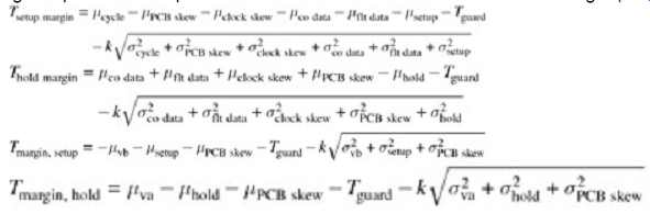
... where µ is the timing mean, s the standard deviation, and k the number of standard deviations (i.e., k = 3 refers to a 3s spread). Equations (1) and (2) are for common-clock buses and (3) and (4) are for source synchronous buses.
It should be noted that these equations assume that the distributions are approximately normal (Gaussian) and that the timing components are completely independent of each other. Technically, neither of these assumptions is correct in a digital design; however, the approximations are close enough to assess the risk of a failure. If the engineer understands these limitations and uses the worst-case spreadsheet as the primary tool, the statistical equations can be a powerful asset. Furthermore, the equations below represent only one way to implement a statistical spreadsheet, a resourceful engineer may come up with a better method. Equations (1) through (4) can be compared directly to the equations derived in Section 8. However, note that there is no jitter term because the jitter is included in the statistical variation of the cycle time. Notice the tester guard band (Tguard) term is not handled statistically. This is because the statistical accuracy of the testers is usually not known.
The most significant obstacle in using a statistical timing spreadsheet is determining the correct statistical means and distributions of the individual components. This becomes especially problematic if portions of the system will be obtained from numerous sources. For example, PCB vendors each have a different process, which will provide different mean velocities and impedance values with different distribution shapes. Furthermore, the statistical data for a given vendor may change. Sometimes, however, the statistical behavior can be estimated. For example, consider a PCB vendor which claims that the impedance of the PCB board will have a nominal value of 50 ohm and will not vary more than ±15%. A reasonable assumption would be to assume a normal distribution and that the ±15% points are at three standard deviations (3s). Approximations such as this can be used in conjunction with Monte Carlo simulations to produce statistical approximations of flight time and skew. Alternatively, when uniform distributions are combined in an interconnect simulation using large Monte Carlo analysis, the result usually approximately resembles a normal distribution. Subsequently, the interconnect designer could approximate the statistical parameters of flight time or flight-time skew by running a large Monte Carlo analysis where all the input variables are varied randomly over uniform distributions bounded by the absolute variations. Since the resultant of the analysis will resemble a normal distribution, the mean and standard deviation can be approximated by examining the resultant data. Numerous tools, such as Microsoft Excel, Mathematica, and Mathcad, are well suited to the statistical evaluation of large data sets. It is possible that the statistical technique described here may have some flaws; however, it is adequate to approximate the risk of a failure if the worst-case spreadsheet shows negative margin.
Ideally, the designer would be able to obtain accurate numbers for the mean and standard deviation for all or most of the variables in the simulation (i.e., PCB Zo, buffer impedance, input receiver capacitance, etc.). Monte Carlo analysis (an analysis method available in most simulators in which many variables are varied fairly randomly and the simulated results are observed) is then performed with a large number of iterations. The resultant timing numbers are then inserted into the statistical spreadsheet. Note that similar analysis is required from the silicon design team to determine the mean and standard deviation of the silicon timings (i.e., Tvb, Tva, Tsetup, Thold, and Tjitter). To determine the risk of failure for a design that produces negative margin in a worst-case timing spreadsheet, the value of k is increased from 1 incrementally until the timing margin is zero. This will determine how many standard deviations from the mean timings are necessary to break the design and will provide insight into the probability of a failure. For example, if the value of k that produces zero margin is 1, the probability that the design will exhibit positive margin is only 68.26%. In other words, there is a 31.74% chance of a failure (i.e., a design that produces negative timing margin). However, if the value of k that produces zero margin is 3.09, the probability that the timing margin will be greater or equal to zero is 99.8%, which will produce 0.2% failures. In reality, however, a 3.09s design will probably produce a 99.9% yield instead of 99.8% simply because the instances that will cause a failure will usually be skewed to one side of the bell curve. When considering the entire distribution, this analysis technique assumes that the probability of a result lying outside the area defined by sigma is equivalent to the percentage of failures. Obviously, this is not necessarily true; however, it is adequate for risk analysis, especially since it leans toward conservatism. Typically, in high-volume manufacturing, a 3.0s design (actually, 3.09), is considered acceptable, which will usually produce a yield of 99.9%, assuming one-half of the curve.
FIG. 3 demonstrates how the value of k relates to the probability of an event occurring for a normal distribution. TBL. 1 relates the value of k to the percentage of area not covered, which is assumed to be the percentage of failures.
FIG. 3: Relationship between sigma and area under a normal distribution: (a) k = 1 standard deviation (1s design); (b) k = 3.09 standard deviations (3.09s design).
TBL. 1: Relationship Between k and the Probability That a Result Will Lie Outside the Solution
2. TIMING METRICS, SIGNAL QUALITY METRICS, AND TEST LOADS
After creating the initial spreadsheet with the target numbers, specific timing and signal quality metrics must be defined. These metrics allow the calculation of timing numbers for inclusion into the spreadsheet and provide a means of determining whether signal quality is adequate.
2.1. Voltage Reference Uncertainty
The receiver buffers in a digital system are designed to switch at the threshold voltage.
However, due to several variables, such as process variations and system noise, the threshold voltage may change relative to the signal. This variation in the threshold voltage is known as the Vref uncertainty. This uncertainty is a measure of the relative changes between the threshold voltage and the signal. FIG. 4 depicts the variation in the threshold voltage (known as the threshold region).
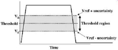
FIG. 4: Variation in the threshold voltage.
Signal quality, flight time, and timing skews are measured in relation to the threshold voltage and are subsequently highly dependent on the size of the threshold region. The threshold region includes the effects on both the reference voltage and the signal. The major effects that typically contribute to the Vref uncertainty are:
---Power supply effects (i.e., switching noise, ground bounce, and rail collapse)
---Core noise from the silicon circuitry
---Receiver transistor mismatches
---Return path discontinuities
---Coupling to the reference voltage circuitry
The threshold region typically extends 100 to 200 mV above and below the threshold voltage.
The upper and lower levels will be referred to as Vih and Vil , respectively. The Vref uncertainty is important to quantify accurately early in the design cycle because it accounts for numerous effects that are very difficult or impossible to model explicitly in the simulation environment. Often, they are determined through the use of test boards and test chips.
2.2. Simulation Reference Loads
In Section 1.1 the concept of a timing spreadsheet is introduced. It is important that all the numbers entered into the spreadsheet (or timing equations) are calculated in such a manner that they add up correctly and truly represent the timings of the entire system. This is done with the use of a standard simulation test load (referred to as either the standard or the reference load). The reference load is used by the silicon designers to calculate Tco times, setup/hold times, and output skews. The system designers use it to calculated flight times and interconnect skews. The reference load is simply an artificial interface between the silicon designer world and the system designer world that allows the timings to add up correctly. This is important because the silicon is usually designed in isolation of the system.
If the silicon timing numbers are generated by simulating into a load that is significantly different from the load the output buffer will see when driving the system, the sum of the silicon-level timings and the board-level timings will not represent the actual system timings.
For example, FIG. 5 shows how simulating the Tco timings into a load that is different from the system can artificially exaggerate or understate the timings of the system. The top portion of the figure depicts the Tco time of an output buffer driven into a load that does not resemble the system input. The bottom portion represents the total delay of a signal in the system (shown as the output buffer driving a transmission
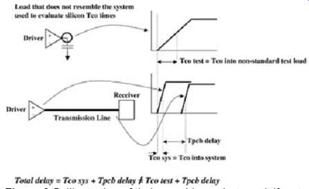
FIG. 5: Illustration of timing problems that result if a standard reference
load is not used to insert timings into the spreadsheet. line). The actual
delay the signal experiences between the driver and receiver in the system
is Tco sys + TPCB delay. If the silicon Tco numbers are calculated with
a load that does not look electrically similar to the system, then the
total delay will be Tco test + TPCB delay, which will not equal Tco sys
+ TPCB delay.
To prevent this artificial inflation or deflation of calculated system margins, the component timings should be simulated with a standard reference load. The same load is used in the calculation of system-level flight times and skews. This creates a common reference point to which all the timings are calculated. This prevents the spreadsheets from incorrectly adding board- and silicon-level timings. If this methodology is not performed correctly, the predicted timing margins will not reflect reality. Since the timing spreadsheets are the base of the entire design, such a mistake could lead to a nonfunctional design. In the sections on flight time and flight-time skew we explain in detail how to use this load.
Choosing a Reference Load.
Ideally, the reference load should be very similar to the input of the system. It is not necessary, however, that the reference load be electrically identical to the input to the system, just similar enough that the buffer characteristics do not change. Since the standard load acts as a transition between silicon and board timings, small errors will be canceled out.
This is demonstrated with FIG. 6. In FIG. 6 the reference load is different from the input to the system. However, since the load is used as a reference point, the total delay is calculated correctly when the timings are summed in the spreadsheet. The top waveform depicts the Tco as measured into a standard reference load. The middle waveform depicts the waveform at the receiver.
The bottom waveform depicts the waveforms at the driver loaded by the system and its timing relationship to the receiver. Notice that if the standard reference load is used to calculated both the flight time and the Tco, when they are summed in the spreadsheet the total delay, which is what we care about, comes out correctly.
This leads us to a few conclusions. First, the flight time is not the same as the propagation delay (flight time is explained in more detail in Section 2.3) and the Tco as measured into the standard reference load is not the same as it will be in the system. The total delay, however, is the same. Note that if the reference load is chosen correctly, the flight times will be very similar or identical to the propagation delays, and the Tco timings will be very similar to what the system experiences.
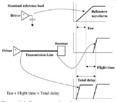
FIG. 6: Proper use of a reference load in calculating total delay.
The reference load for CMOS buffers are often just capacitors that represent the input capacitance seen by the loaded output buffer (if a transmission line was used, there would be a ledge in the reference waveform, which would cause difficulties when calculating timings). This capacitance typically includes the distributed capacitance seen over the duration of the signal edge. For example, if an output buffer with an edge speed of 300 ps is driving a transmission line with a C11 of 2.5 pF/in. and a propagation delay of 150 ps/in., the edge would encompass 2 in. or 5 pF. Subsequently, a good load in this case would be 5 pF. The reference load for a GTL bus usually looks more like the system input because GTL buffers do not exhibit ledges at the drivers as do CMOS buffers when loaded with a transmission line (see Appendix B for current-mode analysis of GTL buffers). FIG. 7 depicts an example of reference loads for a GTL and a CMOS output buffer. The CMOS reference load is simply a capacitor that is equivalent to the system input capacitance seen for the duration of the edge. This will exhibit sufficient signal integrity for a reference load and it will load the buffer similar to the system. The GTL buffer resembles the input of the system. In this particular case, the system is duplicated for the duration of the edge, and the pull-up is included because it is necessary for proper operation. In both cases, typical values should be used for the simulation reference load. It is not necessary to account for process variations when developing the reference load. The simple rule of thumb is to observe the system input for the duration of the edge and use it to design the reference load. Make certain that the signal integrity of the reference load exhibits no ledges and minimal ringing.
It should be noted that this same technique is used to insert timings from a high-volume manufacturing tester into a design validation spreadsheet when the final system has been built and is being tested in the laboratory. The difference is that a standard tester load is used instead of a standard simulation load. However, since it may be impossible to use identical loads for silicon-and system-level testing, simulation can be used to correlate the timings so they add up correctly in the design validation spreadsheet.
2.3. Flight Time
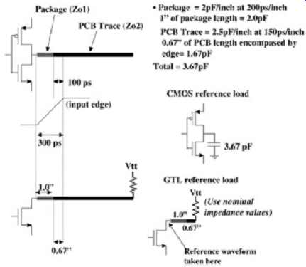
FIG. 7: Examples of good reference loads.
Flight time is very similar to propagation time, which is the amount of time it takes a signal to propagate along the length of a transmission line, as defined in Section 2. Propagation delay and flight time, however, are not the same. Propagation delay refers to the absolute delay of a transmission line. Flight time refers to the difference between the reference waveform and the wave format the receiver (see Section 9). The difference is subtle, but the calculation methods are quite different because a simulation reference load is required to calculate flight time properly so that it can be inserted into the timing spreadsheets.
Flight time is defined as the amount of time that elapses between the point where the signal on an output buffer driving a reference load crosses the threshold voltage and the time where the signal crosses the threshold voltage at the receiver in the system. FIG. 8 depicts the standard definition of flight time. The flight time should be evaluated at Vil , Vthreshold, and Vih. The methodology is to measure the flight time at these three points and insert the applicable worst case into the spreadsheet. It should be noted that sometimes the worst-case value is the maximum flight time, and other times it is the minimum flight time.
For example, the maximum flight time produces the worst-case condition in a common-clock setup margin calculation, and the minimum flight time produces the worst case for the hold margin. To ensure that the worst-case condition is captured, the timing equations should be observed.
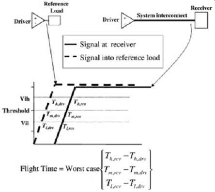
FIG. 8: Standard flight-time calculation.
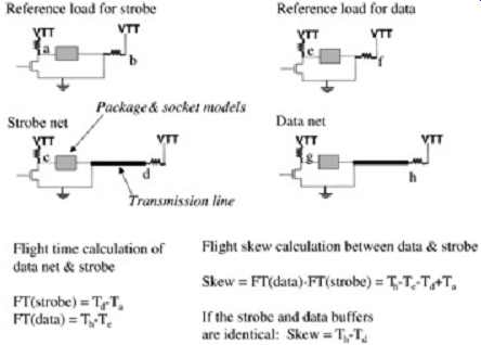
FIG. 9: Simple example of flight-time skew calculation. Note that the
load is identical for data and strobe, but the driving buffer may differ.
A common mistake is to measure flight time from Vil on the reference driver to Vih at the receiver (or from Vih to Vil). This is not correct because it counts the time it takes for the signal to transition through the threshold region as part of the delay. This delay is already accounted for in the Tco variable of the timing equations.
2.4. Flight-Time Skew
Flight-time skew is simply the difference in flight times between two nets. In a source synchronous design, flight-time skew is defined as (5)
It is standard terminology to define skew as data flight time minus strobe flight time. FIG. 9 depicts a generic example of flight-time skew calculation for a GTL bus.
If the timing equations in Section 8 are studied, it is evident that the worst-case condition for hold-time margin is when the data arrive early and the strobe arrives late. The following equation calculates the minimum skew for use in the source synchronous hold equation: (6)
Note that this equation is not sufficient to account for the skew in a real system. Although in the preceding section we warned against calculating flight time across the threshold region, it is necessary to calculate skew (between data and strobe) across the threshold region for conventional source synchronous designs. As described in Section 8, the data and the strobe can be separated by several nanoseconds assuming a conventional source synchronous design. During this time, noise may be generated in the system (i.e., by core operations, by multiple outputs switching simultaneously, etc.) and the threshold voltage may change between data and strobe. Subsequently, it is necessary to calculate skew by subtracting flight times at different thresholds to yield the worst-case results. To do so, the skew is calculated at the upper and lower boundaries of the threshold region. The following equation calculates the minimum skew while accounting for the possibility of noise causing variations of the threshold voltage with respect to the signal: (7)
where Th,rcv is the time at which the signal at the receiver crosses Vih, Th,drv the time at which the signal at the input of the reference load crosses Vih, Tl,rcv the time at which the signal at the receiver crosses Vil , and Tl,drv the time at which the signal at the input of the reference load crosses Vil. Note that even though the skew may be calculated across the threshold region, the flight times are not.
The worst-case condition for source synchronous setup margin is when the data arrive late and the strobe arrives early. The maximum skew for use in the source synchronous setup equations is calculated as
(8)
(9)
2.5. Signal Integrity
Signal integrity, sometimes referred to as signal quality, is a measure of the waveform shape.
In a digital system, a signal with ideal signal integrity would resemble a clean trapezoid. A signal integrity violation refers to a waveform distortion severe enough either to violate the timing requirements of the system or to blow out the gate oxides of the buffers. In the following section we define the basic signal integrity metrics used in the design of a high speed digital system.
Ringback.
Ringback is defined as the amount of voltage that "rings" back toward the threshold voltage.
FIG. 10 graphically depicts a ringback violation into the threshold region as measured at a receiver. The primary effect of a ringback violation into the threshold region is an increase in the flight time. If the signal is ringing and it oscillates into the threshold region, the maximum flight time is calculated at the point where it last leaves the threshold region, as depicted in FIG. 10. This is because the buffer is in an indeterminate state (high or low)
within the threshold region and cannot be considered high or low until it leaves the region.
This can also dramatically increase the skew between two signals if one signal rings back into the threshold region and the other signal does not.
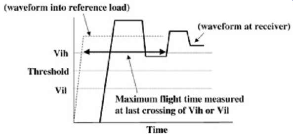
FIG. 10: Flight-time calculation when the signal rings back into the
threshold region.
It is vitally important that strobe or clock signals not ring back into the threshold region because each crossing into or out of the region can cause false triggers. If the strobe in a source synchronous bus triggers falsely, the wrong data will be latched into the receiver circuitry. However, if a strobe that runs a state machine triggers falsely, a catastrophic system failure could result. Ringback is detrimental even if it does not cross into the threshold region. If a signal is not fully settled before the next transition, ISI is exacerbated (see Section 4). Non-monotonic (Nonlinear) Edges.
A non-monotonic edge occurs when the signal edge deviates significantly from linear behavior through the threshold region, such as temporarily reversing slope. This is caused by several effects, such as the stubs on middle agents of a multidrop bus, as in FIG. 16; return path discontinuities, as in FIG. 3; or power delivery problems, as in FIG. 12.
The primary effect is an increase in the effective flight time or in the flight-time skew if one signal exhibits a ledge and the other does not. FIG. 11 shows the effective increase in the signal flight time as measured at Vih for a rising edge.
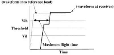
FIG. 11: Flight-time calculation when the edge is not linear through
the threshold region.
Overshoot/Undershoot.
The maximum tolerable overshoot and undershoot are a function of the specific circuitry used in the system. Excessive overshoot can break through the gate oxide on the receiver or driver circuitry and cause severe product reliability problems. Sometimes the input buffers have diode clamps to help protect against overshoot and undershoot; however, as system speeds increase, it is becoming increasingly difficult to design clamps that are fast enough to prevent the problem. The best way to prevent reliability problems due to overshoot/undershoot violation is with a sound interconnect design. Overshoot/undershoot does not affect flight time or skews directly, but an excessive amount can significantly affect timings by exacerbating ISI. FIG. 12 provides a graphic definition of overshoot/undershoot.
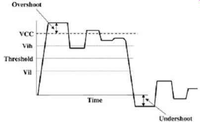
FIG. 12: Definition of overshoot and undershoot
3. DESIGN OPTIMIZATION
Now that the initial timings and the signal quality/timings metrics have been defined, it is time to begin the actual design. First, let's discuss the old method of bus design. FIG. 13 is a flowchart that shows the wrong way to design a high-speed bus. This methodology requires the engineer to route a portion of the board, extract and simulate each net on the board, fix any problems, and reroute. As bus speeds increase and the number of variables expand, this old methodology becomes less efficient. For multiprocessor systems, it is almost impossible to converge using this technique.
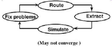
FIG. 13: Wrong way to optimize a bus design.
A more efficient method of design process requires a structured procedure to ensure that all variables are accounted for in the pre-layout design. If this is done correctly, a working layout will be produced on the first pass and the extraction and simulation process is used only to double check the design and ensure that the layout guidelines were adhered to. FIG. 14 depicts a more efficient methodology for high-speed bus design.
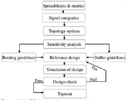
FIG. 14: Efficient bus design methodology.
3.1. Paper Analysis
After the initial timings and the metrics have been defined, the next step is to determine all the signal categories contained within the design. At this point, the engineer should identify which signals are source-synchronous, common-clock, controls, clocks, or fall into another special category. The next portion of the paper analysis is to determine the best estimates of all the system variables. The estimates should include mean values and estimated maximum variations. It is important to note that these are only the initial rough estimates and all are subject to change. This is an important step, however, because it provides a starting point for the analysis. Each of the variables will be evaluated during the sensitivity analysis and changed or limited accordingly. Some examples of system variables are listed below.
---I/O capacitance
---Trace length, velocity, and impedance
---Interlayer impedance variations
---Buffer strengths and edge rates
---Termination values
---Receiver setup and hold times
---Interconnect skew specifications
---Package, daughtercard, and socket parameters
3.2. Routing Study
Once the signals have been categorized and the initial timings have been determined, a list of potential interconnect topologies for each signal group must be determined. This requires significant collaboration with the layout engineer and is developed through a layout study.
The layout and design engineers should work together to determine the optimum part placement, part pin-out, and all possible physical interconnect solutions. The layout study will produce a layout solution space, which lists all the possible interconnect topology options, including line lengths, widths, and spacing. Extensive simulations during the sensitivity analysis will be used to limit the layout solution space and produce a final solution that will meet all timing and signal quality specifications. During the sensitivity analysis, each of these topologies would be simulated and compared. The best solution would be implemented in the final design.
The layout engineer should collaborate with the silicon and package designers very early in the design cycle. Significant collaboration should be maintained throughout the design process to ensure adequate package pin-out and package design. It is important to note that the package pin-out could "make or break" the system design.
Topology Options.
During the layout study it is beneficial to involve the layout engineers in determining which topologies are adequate. FIG. 15 depicts several different layout topologies that are common in designs. It is important to note, however, that the key to any acceptable routing topology is symmetry (see Section 4).
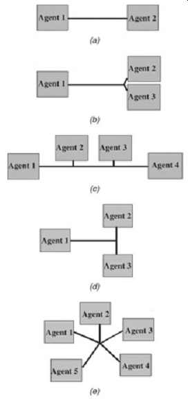
FIG. 15: Common bus topologies: (a) point to point; (b) heavy point to
point; (c) daisy chain; (d) T topology; and (e) star topology.
1. Point to point. This is the simplest layout option. The major routing restrictions to worry about are minimum and maximum line lengths and the ability to match the line lengths in signal groups.
2. Heavy point to point. This topology has the same restrictions as above. Furthermore, the short stubs that connect the main interconnect to the components should be kept very short; otherwise, the topology will behave like a star or T-topology.
3. T topology. T topologies are usually unidirectional; that is, agent 1 (from FIG. 15d)
is the only driver. As mentioned above, symmetry is necessary for adequate signal integrity. The T topology is balanced from the view of agent 1 as long as the legs of the T are the same lengths. Assuming that the legs of the T are equal in length, the driver will only see an impedance discontinuity equal to one-half the characteristic impedance of the transmission lines. If the T is not balanced (such as when agent 2 or 3 is driving), it will resonate and the signal integrity will be severely diminished. If all three legs were made to be equal, the bus would become unidirectional because it would be symmetrical from all agents (then the topology would be a three-agent star, not a T). One trick that is sometimes used to improve T topologies is to make the T legs twice the impedance of the base, which will eliminate the impedance discontinuity at the junction (see Section 4).
4. Star topology. When routing a star topology, it is critical that the electrical delay of each leg be identical; otherwise, the signal integrity will degrade quickly. Star topologies are inherently unstable. It is also important to load each leg the same to avoid signal integrity problems.
5. Daisy chain. This is a common topology for multidrop buses such as front-side buses and memory buses on personal computers. The major disadvantage is the fact that stubs are usually necessary to connect the middle agents to the main bus trunk. This causes signal integrity problems. Even when the stubs are extremely short, the input capacitance of the middle agents load the bus and can lower the effective characteristic impedance of the line as described here.
Early Consideration of Thermal Problems.
After the layout solution space has been determined, it is a good idea to consider the thermal solution or consult with the engineers who are designing the thermal solution. Often, the interconnect design in computer systems are severely limited by the thermal solution.
Processors tend to dissipate a significant amount of heat. Subsequently, large heat sinks and thermal shadowing limit minimum line lengths and component placing. If the thermal solution is considered early in the design process, severe problems can be avoided in the future.