AMAZON multi-meters discounts AMAZON oscilloscope discounts
The purpose of this section is to introduce the reader to the basic techniques used to describe signals, their detection by simple circuits, and their manipulation using signal processing techniques.
Electrical signals are usually voltages that may, however, represent a wide variety of physical processes, e.g., electric field or temperature variations. Similarly, the term "circuits" may be taken to mean a physical system which, when excited in a particular way, responds appropriately.
Hence the material presented in this section is of general value in understanding signals of all types.
A signal is described by a mathematical function, in which the variable is normally time. For example, a voltage source may be described as v(t) = Vpk cos (delta t). This, however, is not the only kind of functional relationship found in EMC work. The function v(t) may take many analytical forms, or may be defined by a set of experimental data obtained at different times. It is necessary, therefore, to separate the exact functional form of v(t) from the more general properties of the signal, and its further processing by hardware (circuits) and software (computer programs) means.
This mathematical description of signals offers great flexibility to the investigator, as it makes it possible to isolate and study specific attributes of the signal and its processing.
Signals may be broadly divided into deterministic and random or stochastic signals. Deterministic signals are those for which the instantaneous value can be specified accurately at each instant of time. These are signals that are used to transmit information and are therefore of primary interest in all applications. There are, however, signals for which even approximate predictions of variation with time cannot be made. These are signals that are due to chaotic thermal fluctuations in circuits and are described as random or stochastic signals. The term "noise" is also used to express the manifestation of these phenomena. A distinction may be drawn between noise, which is generated internally by a circuit, and interference, which is coupled to it from external sources. In cases where the interfering signal is low level, it can sometimes be difficult to distinguish between internally and externally generated unwanted signals and the term "noise" is used indiscriminately to indicate an unwanted signal.
Study of the basic properties of random signals is useful in EMC as it determines the limits of detectability of signals in noisy environments.
In many cases signals may be measured and specified at any instant.
They are then described as continuous (or analog) signals. There are, however, circumstances in which signals are known only at specific instants, multiples of a basic sampling time interval delta_t. They are then known as sampled (or discrete) signals. The magnitude of each sample of a discrete signal may be represented by a binary number. A common representation is to use 8 bits, and thus a pulse train of eight pulses of magnitude 1 or 0 to represent each sample. This signal is then described as a digital signal. Whichever signal representation is chosen, certain general principles apply that permit the description of any complex signal in terms of simpler signals. Examples of such representations are given below.
1. Representation of a Signal in Terms of Simpler Signals
The unit step function is shown in Figure 1a and is defined as
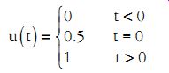
(eqn. 1)
It may be shifted in time to obtain the function u(t - t0) shown in Figure 1b. The signal v(t) shown in Figure 1c may be represented by a succession of step voltages, as shown in Figure 1d. Mathematically, v(t) is then given by the formula:
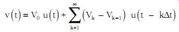
(eqn. 2)
If the sampling interval is made very small and in the limit reduced to zero, this expression reduces to:

(eqn. 3)
Figure 1 (a) A unit step voltage waveform, (b) as in (a) but shifted
by t0, (c) a general waveform and its representation in terms of steps
(d) and impulses (e).
An alternative approach is to represent the signal in Figure 1c as a succession of pulses, as shown in Figure 1e. In the limit, the basic constituent of this representation is the delta function defined by the following properties:
In mathematical form the signal v(t) is then represented by the expression:

(eqn. 4)
Another way of representing a signal is to express it in terms of a number of basis functions, such as sinusoids, in the form (eqn. 5)
It should be noted that only certain signals are suitable as basis signals in Equation 5.
The selection of basis functions fi (t) and the calculation of the coefficients Ci will be explained shortly. However, it is worth pausing to reflect on the significance of Equations 3 to 5. In all cases, the original signal is described in terms of other simpler signals. If the response of a circuit to these simpler signals can be found, and provided that the principle of superposition holds (linear circuit), then the response to the original signal is easily obtained by combining the responses to the simpler signals. A particularly useful formulation is when harmonic signals are used as the basis functions.
A periodic signal v(t) of period T may then be represented in different ways as a collection of harmonic signals, as shown below.
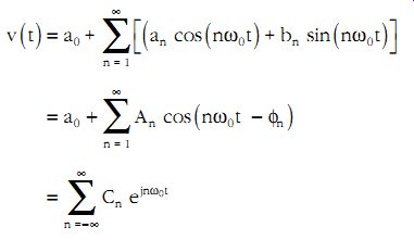
(eqn. 6)
The harmonic functions are all multiples of the fundamental frequency ?0 = 2p/T and this representation of the signal is referred to as an expansion into a Fourier series. The three expressions above are equivalent and the particular choice is a matter of convenience. The unknown coefficients an, bn, An, and Cn may be obtained from the following formulae:
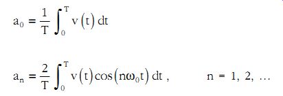
(eqn. 7)
Any periodic signal of period T may thus be represented by a collection of harmonic signals (infinite in number), which have a frequency an integer multiple of ?0 = 2p/T. This is known as a spectral representation of the signal.
To illustrate the application of these formulae, the square wave signal shown in Figure 2a will be studied. Its period is T and the signal is supposed to exist forever! A signal that is zero for t < 0 is clearly not periodic and cannot be represented accurately by a Fourier series. Applying Equation 7 gives...
For the special case when t/T = 0.5 these formulae reduce to...
Thus, for this special case the signal shown in Figure 2a may be represented as follows:
It contains a DC term, first, third, fifth, and so on, harmonics. It is interesting to speculate how many terms are required to describe accurately this signal in terms of its spectral content. Clearly, for higher harmonics (n large) the amplitude decreases and hence contributions are small. The reader may plot the formula above retaining the first three terms only and compare the result with the waveform in Figure 2a. It will be seen that a substantial error remains at the transition between low and high values. This error persists even when many more terms are included in the Fourier series (Gibbs phenomenon).
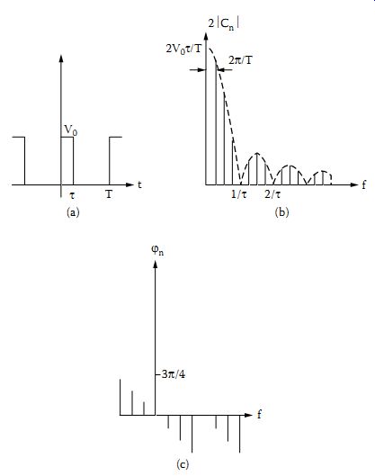
Figure 2 A repetitive pulse waveform (a), its amplitude (b), and phase
(c) spectra.
Let us now visualize in more detail the spectrum of this signal for the general case. The coefficient Cn is easily calculated and is (eqn. 8)
Hence,…
The coefficient Cn is equal to |Cn| ejf n where |Cn| is the magnitude of the term in brackets (Equation 8) and fn = ±n ?0 t/2. The negative sign is selected when n ?0 t/2 < p. In addition, C-n is equal to the complex conjugate of Cn, hence…
Coefficients C0, 2|Cn|, and fn constitute the magnitude and phase spectrum of this signal. The first few terms are plotted in Figure 2b and c.
The shape of the envelope of the magnitude spectrum is that of the function sinx/x, which is tabulated in Appendix C. Naturally, real square wave pulses do not have zero rise- and fall-times as assumed here. The influence of finite rise- and fall-times on the spectra is explained in sect. D. However, it is already possible to gain an insight into the spectral content of this signal. Let us assume that the repetition rate is 50 MHz (T = 1/50 10^6 = 20 nsec) and that the duty cycle is 50% (t = 0.5 T = 10 nsec). Then the fundamental frequency is 50 MHz and the first zero in the magnitude spectrum is at f = 1/t = 100 MHz. It can be seen that at the ninth harmonic (f = 450 MHz) the amplitude is still in excess of 10% of its value at the fundamental frequency. This type of pulse thus contains many frequencies covering the entire range of interest to EMC.
Let us now consider how to deal with signals that are not periodic.
In mathematical terms, an aperiodic signal may be regarded as a periodic signal with very large period (T ? 8). Hence, the last expression in
Equation 6 can be generalized to give the Fourier transform of a signal v(t).
(eqn. 9)
...where...

(eqn. 10)
The essential difference between the spectra of periodic and non periodic waveforms is that in the former the spectrum consists of contributions at distinct frequencies multiples of the fundamental, while in the latter there are contributions at all frequencies, i.e., the spectrum is continuous. As an example, the spectrum of the pulse shown in Figure 3a is calculated. Using Equation 10 and substituting for v(t) gives:
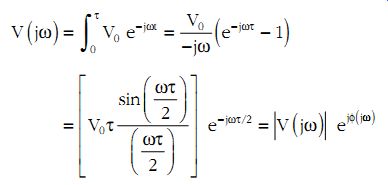
(eqn. 11)
where f(j?) = ±?t/2 and the negative sign is selected when (?t/2) < p.
The amplitude and phase spectra are plotted in Figure 3b and c.
Let us now examine the spectrum of a very-short-duration impulse, such that the product of its amplitude and duration is equal to A. This is referred to as a delta function pulse, and mathematically is described by the following formula.
Substituting into Equation 10 gives…
Thus, the delta impulse has a flat spectrum. Applying a very-short-duration pulse is like injecting signals at all frequencies having the same magnitude and phase. The value of this so-called impulse excitation is that it contains within it the entire spectrum of signals.
In practical situations, it is difficult to generate pulses of zero rise- and fall-times. It is therefore useful to study the spectrum of signals with a smooth transition from zero to the peak voltage value. A particularly useful signal of this type is the Gaussian pulse defined as:

(eqn. 12)
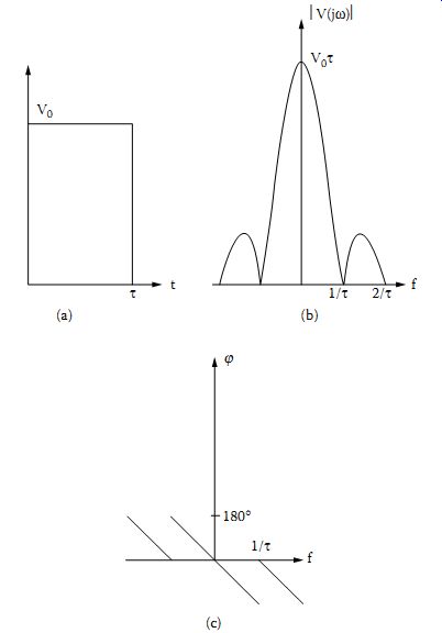
Figure 3 A pulse (a), its amplitude (b), and phase (c) spectra shown
up to a frequency 2/t t t t.
The effective duration of this pulse td is defined as the time interval in which the pulse exceeds 10% of its peak value. It can be shown that td =3/ The spectrum of this pulse is found to be:
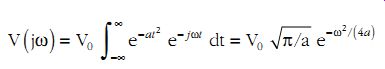
(eqn. 13)
Thus, the spectrum is also a smooth function of frequency of the same shape as the pulse.
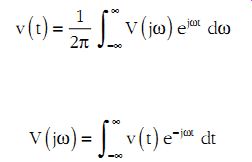
The pair of transforms described by Equations 4.9 and 4.10 offers two alternatives for the study of signals. First, a signal may be described as a function of time or in what is referred to as the time domain. If the time variation of the signal is a complicated one, it is normally very difficult to proceed directly by calculation to find the response of circuits to it.
Second, an alternative approach may be adopted whereby the spectral content V(j?) of the original signal v(t) is found using Equation 10. The response of a circuit to v(t) can then be studied by reference to its response to the spectral components V(j?). This approach is normally easier to pursue, especially for signals with complicated time waveforms. The spectrum V(j?) of the signal contains complete information about it and may be regarded as its description in the frequency domain. Conversion between the time and frequency domains is achieved by using the direct (Equation 10) and inverse (Equation 9) Fourier transforms. It can be shown that
(eqn. 14)
This equation, referred to as Parseval's Theorem, relates measures of energy associated with signal description in the time and frequency domains. A plot of |V(j?)|2 vs. frequency is described as the power spectrum of the signal.
Examination of Figure 3 shows that a decrease in the duration of a pulse (t small) results in a broad spectrum of frequencies (l/t increases), i.e., a narrow pulse implies a wide bandwidth and vice versa. In broad terms it can be stated that the product of signal duration in the time domain td and of its bandwidth (BW) in the frequency domain is of the order of 1, i.e.,

(eqn. 15)
Let us now study the spectrum of a more complex waveform, such as the one shown in Figure 4a. Clearly, this waveform may be regarded as the product of the two waveforms shown in Figure 4b and c. The spectrum of the waveform (b) can be obtained easily.
Hence...
This integral can be evaluated if the sampling property of the delta function is invoked, i.e.,...
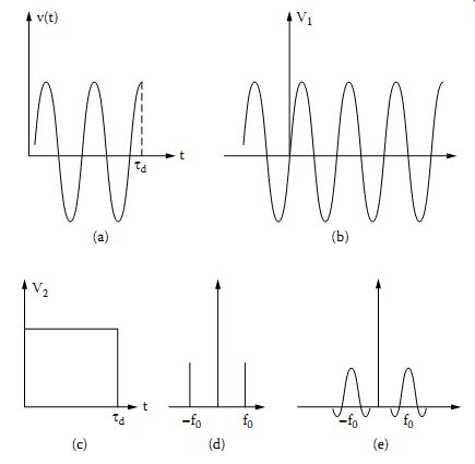
Figure 4 A sinusoidal signal of finite duration (a) and its derivation
from a periodic signal (b) and pulse (c). The spectrum of V1 (d) and of
v(t) (e).
This means that the Fourier transform of is 2pd (? - ?0). Using this result in the expression for V1(j?) gives (eqn. 16)
Thus, the amplitude spectrum of V1(t) consists of two contributions of ±?0 as shown in Figure 4d. The spectrum of v2(t) has already been obtained (Figure 3b).
The question arises whether the spectrum of the waveform shown in Figure 4a may be obtained from the spectra of v1(t) and v2(t). It turns out that this is the case, but while v = v1(t) v2(t), the spectrum V(j?) ? V1(j?) V2(j?). Instead the following expression holds:

(eqn. 17)
The integral on the right-hand side of Equation 17 is called the convolution of waveforms V1(j?) and V2(j?) and it is normally indicated using the notation V1(j?) * V2(j?).
Substituting into Equation 17 for V1(j?') gives:

(eqn. 18)
This expression indicates that the spectrum of v(t) consists of the spectrum of the rectangular pulse shifted by ±?0, as shown in Figure 4e.
Several conclusions may be drawn from these spectra. If the duration of the co-sinusoidal wave is long (td >>), then its spectrum shown in Figure 4e becomes very narrow around ±?0 and tends to that of a waveform of infinitely long duration. If only a few periods of the signal are included (td <<), then the spectrum contains very substantial contributions at frequencies other than ?0.
Figure 5 Autocorrelation of the signals in (a) and in (c), shown in (b) and (d), respectively.
2. Correlation Properties of Signals
There are many applications that are critically dependent on evaluating the degree of similarity between two signals or, in technical parlance, their correlation. A particular example of this is in radar. The correlation properties of signals are described in this section.
2.1 General Correlation Properties
The autocorrelation of a signal v(t) is defined as the quantity…

(eqn. 19)
…where the signal v(t - t) has the same functional dependence as signal v(t) but it is shifted in time by an amount t. For the signal shown in Figure 5a, the autocorrelation is shown in Figure 5b. Similarly, the autocorrelation of the signal in (c) is given in (d). It can be shown that the power spectrum |V(j?)|2 of a signal and its autocorrelation function are Fourier transform pairs (Wiener-Khinchine Theorem). From this it follows that the wider the frequency spectrum of a signal is, the narrower the width of its autocorrelation function will be and the easier it will be to locate it in time. Under some circumstances it may be easier to obtain the power spectrum of a signal by first finding its autocorrelation and then its Fourier transform.
A measure of the similarity between two signals is provided by their cross-correlation, defined as (eqn. 20) It can be shown that the cross-correlation of two signals is related to their spectra by the expression (eqn. 21) where the star * indicates the complex conjugate quantity.
2.2 Random Signals
Random signals and their mathematical description is an extensive subject that cannot be covered fully in this text. However, it is necessary to get a basic idea of random signals, which manifest themselves as noise in many systems. It may be thought that random signals, by their nature, cannot be described in any precise way. Although this is true as far as predicting their precise evolution in time is concerned, it does not, however, prevent us from making precise statements about them, which are true in a statistical sense.
Let us consider a quantity x varying randomly, with a probability P(x) that this quantity has a particular value x. Then the mean or expected value of x, designated as <x>, is:

(eqn. 22)
Similarly, the mean square value of x is:

(eqn. 23)

(eqn. 24)
The square root of the variance is called the standard deviation sx of the signal x. For most signals encountered in engineering applications, the averaging indicated by Equations 22, 23, and 24 may be replaced by a time-average over a period of time T, which tends to infinity (ergodic signals), i.e., A representation of a random signal in the time domain has a corresponding description in the frequency domain. It will be assumed here that the statistical characteristics of a random signal remain unchanged with respect to time (stationary random signal). The autocorrelation of such a signal is defined as

(eqn. 25)
It will be seen from this expression and from Equation 24, that provided the mean value of x(t) is zero, then = R(0).
The autocorrelation of a random signal v(t) and its power spectrum Wv(j?) are a Fourier transform pair, i.e.,
(eqn. 26)
This is known as the Wiener-Khinchin Theorem. It follows that the variance of the signal is
(eqn. 27)
A particularly useful random signal is "white noise," defined as a signal with a constant power spectrum at all frequencies, i.e., Wwn(j?) = W0.
For this signal, the variance may be obtained from Equation 27 and is (eqn. 28) The rms value of the signal associated with the white noise is equal to the square root of the variance. From the first of the set of Equation 26 it follows that the autocorrelation of white noise is
Figure 6 Impulse (a) and frequency (b) response of a system.
3. The Response of Linear Circuits to Deterministic and Random Signals
The response of linear circuits to a variety of inputs can be described in several ways. Two particular techniques used frequently are to find the circuit's impulse and frequency response. These two cases are examined below.
3.1 Impulse Response
The impulse response h(t) of a circuit is the output obtained when the input signal is a delta function. In practice, the impulse applied at the input must have a duration much shorter than the shortest time constant of the circuit. If the impulse response h(t) is known, then the output to any input signal is equal to the convolution of h(t) and the function describing the input signal (Figure 6a), i.e.,

(eqn. 29)
3.2 Frequency Response
An alternative approach is to find the frequency response of the circuit H(j?) to harmonic inputs covering the entire frequency range of interest.
The phasor describing the output signal at a particular frequency is given by the expression:
(eqn. 30)
...as shown in Figure 6b.
To find the response to an arbitrary input, the spectrum of the input signal is first determined using Fourier transforms. The output to each frequency component is then obtained from Equation 30 and thus the spectrum of the output signal is found. The output voltage in the time domain can then be obtained by taking the inverse Fourier transform of the output spectrum.
The impulse and frequency responses h(t) and H(j?), respectively, are Fourier transform pairs. Either of these two functions describes fully the response of the circuit. An alternative method for determining the impulse response of a linear system is to exploit the property that the input-output cross-correlation is equal to the convolution of the impulse response and the input autocorrelation.
The input-output cross-correlation is defined as
Rin/out = <vin(t) vout (t + t)>.
If the input to the system is supplied with white noise [autocorrelation W0d(t)] and the input-output cross-correlation is measured, then h(t) = Rin-out (t)/W0. This approach has several advantages.
The following simple example will help to illustrate the techniques described above.
Example 1: Find the frequency and impulse responses of the circuit shown in Figure 7 and then obtain an expression for the output voltage when the input is a step voltage V0.
Solution: The frequency response is easily obtained:
Hence......
Figure 7 Circuit used to study the relationship between frequency and impulse response.
The impulse response is obtained from Fourier transform tables (inverse transform of H(j?)) and is.... Working in the frequency domain the output voltage is then....
Hence, from Fourier transform tables...
Working in the time domain, the output voltage is...
As expected, the same expression for the output voltage is obtained whichever approach is adopted. This general procedure can be easily adapted to work with sampled signals.
The rms value of the output voltage is equal to the square root of the variance, i.e., .
3.3 Detection of Signals in Noise
Strategies have evolved to detect signals that are mixed with noise. The objective is to design circuits that are capable of detecting signals in an optimum manner. The theory relevant to this task is known as optimum filtering.
A particular example will be presented here, whereby characteristics of a filter are desired that are capable of maximizing the ratio of signal to noise at its output. It is assumed that the input signal waveform is known and that the output signal is mixed with white noise.
Let us assume that the input voltage waveform is known, vin(t), and that its frequency spectrum is...

(eqn. 31)
The white noise at the input has a power spectrum W0. Let us also assume that the desired frequency response of the filter is (eqn. 32) The variance of the noise signal at the output of the filter is then given by Equation 33:

(eqn. 33)
Maximizing the ratio of the output signal at a particular time t0 to the square root of the variance of the noise at the output requires the following filter frequency response:

(eqn. 34)
…where A is a constant.
It can also be shown that the impulse response of the filter is h(t) =
A V1 (t0 - t), i.e., it is, but for a scale factor, a mirror image of the input signal about the t = 0 axis, shifted by an amount of time t0. This type of filter is known as a "matched filter" as it is clearly matched to perform optimally for a particular input waveform. The output voltage due to v1(t) is given by the inverse Fourier transform of V2(j?) = H(j?) V1(j?), hence…
(eqn. 35)
The quantity on the right may be recognized from Equation 26 as the autocorrelation of the input signal, i.e.,

(eqn. 36)
Figure 8 Input signal (a), its autocorrelation (b), and output signal (c).
Taking as an example the input waveform shown in Figure 8a, its autocorrelation function is then as shown in Figure 8b and the output signal as in Figure 8c, where it was chosen to maximize the ratio of signal to noise at the time the input waveform goes to zero (t0 = td).
Clearly, the output waveform for this matched filter is very different to the input waveform. The objective is maximizing the chances of detecting the signal from the noise and not its faithful reproduction. This situation typically occurs in radar applications. Using Equations 4.33 and 4.34 the variance of the noise at the output is found to be…
The integral on the right is related to the energy associated with the input pulse, hence from Equation 14,...
At the moment when the ratio of signal to noise is maximum, the output signal is from Equations 35 and 14:
Hence, the ratio of signal to noise is....
....and it is seen to depend on the energy associated with the signal It is customary to accept a minimum acceptable ratio of signal to noise for adequate detection of about three. Based on this assumption the required magnitude of the signal at the input is V0 = 3 W0 · td.
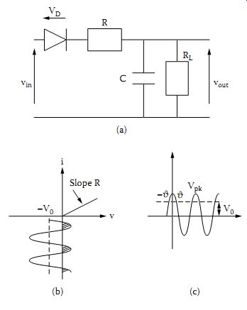
Figure 9 A nonlinear detector (a), current (b), and voltage (c) waveforms.
4. The Response of Nonlinear Circuits
Nonlinear circuits are frequently used in engineering applications. Their main utility is to add to input signals other frequency components. Whereas in linear circuits the principle of superposition holds, the same cannot be said of nonlinear circuits. Thus, circuit analysis in nonlinear circuits is more difficult. A simple example is presented here to illustrate some of the solution principles and also introduce a particular circuit used often as a detector.
A circuit configuration used to detect signals is shown in Figure 9a.
The circuit consists of a diode and charging (R - C) and discharging (RL - C) circuits. The load resistance is RL and R represents the diode forward resistance. The detector circuit may be given different characteristics by varying the relative magnitude of charging and discharging time constants. If, for instance, the charging time constant tc = RC is much larger than the discharging time constant tD = RLC, then the detector output is sensitive to the peak value of the input signal. If, however, this inequality does not hold, then the detector does not quite respond to the peak and it is described as a quasipeak detector. A low-pass filter after the detector produces an output proportional to the average of the signal. Similarly, modifications may be introduced to produce the rms value of the input signal.
For illustration purposes the response of the circuit shown in Figure 9a to a sinusoidal input signal of frequency ?0 and peak amplitude Vpk will be studied. Other cases are presented in detail in Reference 6. Let us assume that the DC component of the output current is I0. Then the voltage across the diode is VD = Vin - I0RL. Assuming an idealized diode characteristic, then charging current flows during the period indicated by the hatched waveform in Figure 9b. The DC component of the current is related to the DC component of the hatched voltage waveform V' by the expression I0 = V'/R. From Figure 9c it is clear that V0 = Vpk cos ? and hence ? = arc cos (V0/Vpk). Using Equation 7, the DC component V' is obtained as shown below:
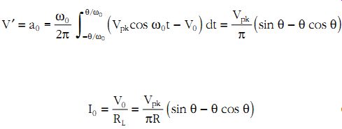
(eqn. 37)
(eqn. 38)
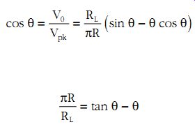
If the circuit parameters are such as to give, say, tD/?c = RL/R = 2400, then ? is very small then tan ? may be approximated by the first two terms in its Taylor series expansion.
Substituting the above expression in Equation 38 gives....
For the case chosen RL/R = 2400, it follows that ? = 0.158 rad and therefore V0/Vpk = cos ? = 0.987. The DC component of the output voltage is virtually equal to the peak input voltage. The relationship between the two time constants may be varied to give different characteristics to the detector. In EMC applications, peak and quasipeak detectors are common.
The latter has a relatively short discharge time constant to produce a lower output for input pulses occurring infrequently. This is aimed at producing a measure of interference that is related to the relative annoyance caused to listeners of radio signals that are subject to frequent and infrequent pulses of similar magnitude. Descriptions of the different types of detector in use may be found in References 7 and 8.
5. Characterization of Noise
Noise may be due to many causes both external (e.g., galactic noise) and internal (e.g., Johnson noise) to a system. More details of the spectral properties of noise sources are given in section 5. Irrespective of the origins of noise, it is necessary to establish a set of parameters that allows quantitative results in regard to noise to be determined for a variety of networks. A more detailed description of noise and its characterization may be found in References 9 to 11. Let us first examine the noise that may be expected at the terminals of an antenna.
An antenna placed in an enclosure of temperature T is surrounded by a low-level electromagnetic field that is the result of random fluctuations.
The flux of electromagnetic energy at a given point coming from a solid angle of one steradian is given by Planck's formula and is 12
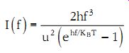
(eqn. 39)
I(f) is given in units of Wm-2 Hz-1 srad-1, f is the frequency, u the speed of light, and h = 6.626 · 10^-34 J/Hz is Planck's constant. In most practical cases hf << KBT and therefore ehf/KBT _ 1 + hf/KBT. Equation 39 thus reduces to....

(eqn. 40)
....where ? is the wavelength. This is known as Rayleigh's Law. Let the mean square value of the electric field strength per hertz be <E2> = <E2 > x + <E2 > y + <E2 > z , where the right-hand side indicates the field contributions in each coordinate direction. On average these are expected to be at the same value, hence <E2> = 3<E2> z . The power flux associated with the EM field may be found from Poynting's vector and for air is....
The power flux per steradian is thus....
Equating this with the value obtained from Equation 40 gives for the z-directed electric field component....
For a short antenna of length l polarized in the z-direction, the induced voltage will be....
Substituting the radiation resistance for this dipole from Equation 2.68 gives (eqn. 41).
This formula gives the square of the rms voltage per hertz appearing across the antenna terminals due to EM field fluctuations. The temperature T in this formula represents the regions of space through which EM waves propagate and ranges from a few degrees Kelvin to several thousand degrees in the direction of radio galaxies and is referred to as the antenna noise temperature. For an antenna with Rrad = 5 ?, T = 20 K, and system bandwidth 30 MHz, the rms noise voltage is 0.4 µV.
It turns out that, irrespective of the physical origin of the resistance, Equation 41 applies, where the temperature is that at which the particular resistance is kept (Johnson thermal noise). Although the rms value of thermal white noise is specified in Equation 41 and is , its instantaneous value varies statistically according to a Gaussian probability distribution. The probability that the instantaneous voltage lies between V and V + dV is...
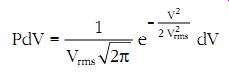
(eqn. 42)
Figure 10 Equivalent circuit of a "noisy" resistor connected to a device with input resistance Ri.
If a real resistor R is connected to a circuit that presents an input resistance Ri , then some of the noise associated with R will couple to the circuit through Ri. We may then represent the real resistor R by an ideal noiseless resistor R in series with a noise source as shown in Figure 10 where we have indicated the RMS value measured over a bandwidth (BW). Maximum power transfer to the load (Ri in this case) occurs when the load impedance is the complex conjugate of the source impedance.
In the present case this corresponds to the condition Ri = R. Thus the maximum available noise power from the resistor R is....
Substituting the RMS value from (eqn. 41) we obtain where BW is the bandwidth of the circuit (the noise power spectral density is KBT). If as an example we calculate the available noise power over a ....bandwidth of 1 Hz at room temperature (say T = 290 K) we obtain Pmax =4 × 10^-21 W. Referring to 1 mW and expressing in decibels gives a maximum available power of ....
This is the minimum achievable noise level at room temperature (noise floor). This noise floor can only be reduced further by cooling equipment below room temperature. It is also pointed out that there are other sources of noise (in addition to thermal noise described above), hence the noise floor is likely to be even higher.
Every device or network used for signal processing receives the desired signal plus noise and produces at its output the modified signal plus noise.
At each stage of this process the signal-to-noise ratio (SNR) may be defined as....

(eqn. 43)
…where S is the power associated with the signal and N is the power associated with noise. Clearly, a high signal-to-noise ratio guarantees good signal reception and detection. Which value of SNR is acceptable depends to a large extent on the application. For TV reception, values in excess of 40 dB are required for good picture quality. For voice communication of good quality, values in excess of 30 dB are required. It is considered just possible to establish communication between experienced operators at SNR values of 5 dB.
Every device, such as an amplifier, adds its own noise component to the signal and hence the signal-to-noise ratio at its input and output are not the same. A measure of the noise introduced by a device is given by its noise factor, defined as follows:
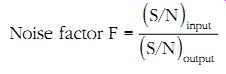
(eqn. 44)
If Ns is the source noise power and Na the noise power added by the device per hertz, then (eqn. 45)
The noise figure of the device is defined as Noise figure NF = 10 log F, dB (eqn. 46) A low-noise amplifier has typically a noise figure less than 3 dB.
Another way to describe the noise added by a device is to assign to it an "effective noise temperature" Te. This is defined as the temperature of a fictitious additional source resistance connected at the input of the device that gives the same noise power at the output. The device is now assumed to be noiseless. Thus, the noise equivalent circuit of a device where the source impedance is Rs is as shown in Figure 11. From Equation 45 it can be seen that the noise factor and the noise temperature are related by the expression...
(eqn. 47)
...where T0 is the temperature of the source resistance (usually the ambient temperature).
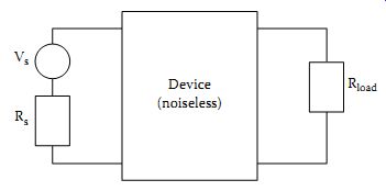
Figure 11 Noise equivalent circuit of a device.
Example: An antenna has a noise temperature of 25 K and is connected to a receiver of noise temperature 30 K. Assuming that the minimum accept able SNR at the output of the receiver is 5 dB, calculate the minimum acceptable signal power at the input of the receiver. A bandwidth of 10 kHz may be used in the calculation.
Solution: The noise factor of the receiver is where T0 was taken as the ambient temperature 20ºC. Hence,
....
Therefore, the minimum acceptable input signal power is 1.38 × 10^-17 W.
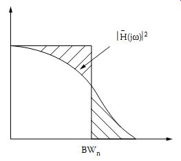
Figure 12 Equivalent noise bandwidth.
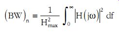
It remains now to examine more carefully how the bandwidth of a system may be determined, specifically for noise calculations. If a wide band noise signal is applied to a frequency-selective network such as a filter or tuned amplifier, the spectrum of the noise at the output follows the shape of the frequency response of the networks. The question often raised is, what is an appropriate bandwidth (BW)n to use in calculating the total noise power at the output? This equivalent-noise bandwidth (BW)n is defined as the bandwidth of an idealized network with a rectangular response that produces the same noise power at the output as the real network. This is shown in Figure 12, where the condition mentioned above is met provided the two hatched areas are equal. It follows that if the input noise spectral power density is Wn (V2/Hz), then…
…or that the equivalent noise bandwidth of a network of frequency response H(j?) (peak value Hmax) is...
(eqn. 47)
For a simple RC network... Hence, Hmax = 1 and... Substituting in Equation 47 gives the following expression for the equivalent-noise bandwidth of an RC circuit...
(eqn. 48)
This should be compared with the bandwidth (BW) of this network defined as the point at which the frequency response falls to 1/ of its peak value (3-dB point), which is (BW) = l/2pRC. Hence, for this network

(eqn. 49)
Figure 13 Schematic to calculate the noise at the output of a system with noise figure NF.
The relationship between noise and normal bandwidths depends on the exact shape of H(j?). Equation 49, however, still holds, approximately, for a range of tuned networks with simple bell-shaped responses.
Example: Calculate the equivalent noise bandwidth and the noise voltage at the output of a tuned amplifier with resonant frequency 1 MHz, quality factor Q = 50, and gain at resonance G = 60. Assume that white noise is injected at the input with W0 = 10^-8 V2/Hz and that Equation 49 holds for this network.