AMAZON multi-meters discounts AMAZON oscilloscope discounts
Signal-generator circuits produce RF sine-wave (or other waveform) output for purposes of testing, troubleshooting, and alignment. Although the subject of designing top-notch signal generator circuits can be quite deep, it is possible to reduce the possibilities to a small number for people whose needs are less stringent. This section looks at RF signal generators that can be used in a wide variety of applications on the electronic and radio workbenches. But first, take a look at some generic types of oscillator circuits.
Types of oscillator circuits
The two major categories of oscillator circuits in electronics textbooks are relaxation oscillators and feedback oscillators. The relaxation oscillator uses some sort of voltage-breakdown device, such as a neon glow-lamp or unijunction transistor.
The feedback oscillator (Fig. 1) uses an amplifier circuit and a feedback network to start and sustain oscillations on a particular frequency. Most oscillators that are useful for sine-wave signal generator circuits are of the feedback oscillator class.
The requirements for sustained oscillator, called Nyquist's criteria, are (1) the loop gain between feedback network losses and amplifier gain must be greater than or equal to one at the frequency of oscillation and (2) the feedback signal must be in phase with the input signal at the frequency of oscillation. The second of these criteria means that the feedback signal must be phase-shifted 360 deg., of which 180 deg. is usually obtained from the inversion of the amplifier and 180 deg. from the frequency selective feedback network.
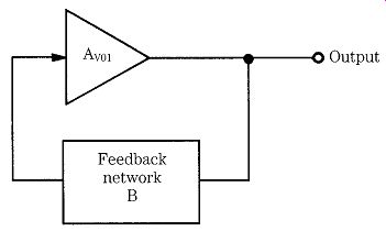
FIG. 1 Feedback oscillator block diagram.
Feedback oscillators can also be classified according to the nature of the feed back network. The three basic types of feedback oscillators (and many variations on the themes) are Armstrong, Colpitts or Clapp, and Hartley. Other forms of feed back network are used at audio frequencies, but these are the principal forms of RF oscillators. You can tell which is which by looking at the feedback network (Fig. 2). The Armstrong oscillator (Fig. 2A) uses a separate tickler coil (L2) to provide feedback to the main tuning coil (L1). These coils are usually wound on the same coil form with each other. The Colpitts oscillator (Fig. 2B) uses a parallel resonant-tuned circuit and (this is the key) a tapped capacitor voltage divider (C1 and C2) to provide feedback. The voltage divider might be a direct part of the resonant circuit. The Clapp oscillator is a variant of the Colpitts circuit, in which a series resonant tuning circuit is used. Finally, the Hartley oscillator uses a tapped inductor voltage divider (Fig. 2C) for the feedback network.
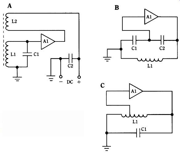
FIG. 2 Feedback oscillator circuits: (A) Armstrong, (B) Colpitts, and (C)
Hartley.
The resonator of the oscillator could be either an inductor-capacitor (LC) tuned circuit, as shown in the examples of Fig. 2, or a piezoelectric crystal resonator.
The latter are single-channel resonators, but are more stable than LC-tuned circuits.
1- to 20-MHz crystal oscillator
FIG. 3 shows a simple, nearly universal signal generator that can accommodate crystal frequencies between 1 and 20 MHz. This oscillator operates in the fundamental mode so the marked frequency of the crystal is the actual frequency that it operates on (as opposed to overtone crystals that operate on harmonics of the fundamental frequency). When specifying the crystal, if you are given a choice, ask for a crystal that operates into 32 pF of capacitance. Otherwise, the actual operating frequency might be a little different than the specified frequency.
The amplifier device is a simple bipolar NPN transistor. The transistor selected is not critical, but the 2N3904 and 2N2222 devices have been tried on numerous occasions in this circuit. Whatever transistor is selected, it must operate as an oscillator in the frequency range of interest. If you want to use a similarly rated PNP transistor (e.g., 2N3906), then simply reverse the polarity of the dc power supply. The transistor uses the simplest form of dc bias network: R1 is directly connected between the transistor's collector and its base. The output signal is taken through a dc-blocking capacitor (C5) across the emitter resistor (R2). A bypass capacitor (0.01 to 0.1 uF) is connected between the collector and ground. This capacitor sets the collector at ground potential for ac potentials and keeps it at the rated dc power-supply potential (9 to 12 Vdc).
The feedback network consists of capacitors C1 and C2. The ratio of the values, C1/C2, is selected to achieve a reasonable tradeoff of output level and stability. These capacitors should be either silver mica or (preferably) NP0 disk ceramic capacitors.
Use of these types of capacitor will prevent frequency drift of the oscillator as a result of temperature-dependent changes in the capacitance of C1 and C2. For the same reason, capacitor C3 should also be a silver mica or NP0 disk ceramic.
The circuit as shown in Fig. 3 operates at a single frequency because it is crystal controlled. Although it's nice to think that the crystal always operates on the specified frequency, it's likely that differences in circuit capacitance will make it oscillate at a different frequency. If the exact frequency is important then replace C3 with a variable capacitor. Alternatively, connect a 50-pF variable capacitor in parallel across the crystal.
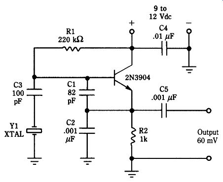
FIG. 3 Colpitts crystal oscillator.
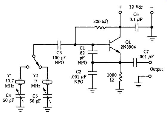
FIG. 4 FM alignment oscillator. Use 10.7 MHz for IF alignment and 9-MHz to
align lo cal oscillator at 90, 99, or 108 MHz.
The circuit of Fig. 3 is popular with people who have to troubleshoot FM radio receivers. FIG. 4 shows a signal generator that can be used to align and test common FM radio receivers. The basic circuit is the same as Fig. 3, but the crystal is replaced with a SPDT switch and a pair of crystals. The 10.7-MHz crystal is used to test the FM IF amplifier stages, so it is on the standard FM IF frequency. The 9-MHz crystal is used to test the front-end and tuning dial accuracy of the receiver.
A 9-MHz crystal will output sufficient harmonics at 90, 99, and 108 MHz to check the calibration of the low end, middle, and high end of the dial, respectively. Notice that this signal generator does not produce an audio tone in the output of the receiver but rather it is indicated by "quieting" of the receiver and an increase in the strength meter reading.
HF/VHF buffer amplifier
A buffer amplifier is used to isolate the output of the oscillator from the load, or circuits that follow. Variations in the load of an oscillator can "pull" the frequency in correctly so the buffer is used to prevent that problem. FIG. 5 shows the circuit for a buffer amplifier that can be used in the low-frequency (LF), high-frequency (HF), and the lower end of the VHF ranges.
The amplifier device in the buffer amplifier is a 40673 dual-gate MOSFET transistor (or NTE-222, which is a replacement). The MOSFET is connected in the standard "grounded source" (S) configuration. A small source bias is provided by the 100-ohm resistor (R2) from source to ground. A 0.1-uF capacitor shunted across R2 keeps the source resistor at ground potential for RF signals while also keeping it at the small positive dc potential caused by the voltage drop across the resistance.
The positive operating dc potential on the drain (D) is supplied through a 270-ohm collector load resistor (R3) and a 1000-uH radio-frequency choke (RFC1). The choke has an inductive reactance that increases linearly with frequency, so the combination of R3 and RFC1 provides a load impedance that increases with frequency, overcoming the tendency of the transistor to offer less gain at higher frequencies.
The dc drain load network (R3/RFC1) is decoupled by a pair of 0.1-uF bypass capacitors. Use disk ceramic, polyester, or other forms of capacitor for this application, but be sure when ordering them that they will work as bypass capacitors at the low-VHF region (see the write-up in the catalog at the beginning of each section on capacitors).
The input is applied through a dc-blocking capacitor (C1), across a gate resistor (R1), to MOSFET gate G1. The output signal is taken from the drain (D) through a 0.001-uF dc-blocking capacitor (C3).
The second gate (G2) of the 40673 MOSFET is biased to a potential of about 10 Vdc, which is set from the +12-Vdc power supply by voltage divider R4/R5. The G2 terminal is set to ac ground by a bypass capacitor (C4) selected to have a low capacitive reactance at the minimum operating frequency relative to R5. In practical terms, this means that XC4 + R5 /10.
A variation on the theme can be built by connecting the voltage divider network R4/R5 to a potentiometer or other variable voltage source instead of the V_ power supply (as shown). The variable voltage can then be used as an output level control.
In some signal generators, the G2 terminal of the MOSFET buffer amplifier is connected to an automatic gain control (AGC) to stabilize the output signal level.
Another use for the G2 terminal is to amplitude modulate (AM) the output signal level. A potentiometer and capacitor (see inset to Fig. 5) is used to connect the G2 circuit to an audio sine-wave source. Be sure that the sine-wave amplitude is high enough to make the amplifier nonlinear (otherwise modulation will not result) but not so much that the output waveform peaks and valleys do not "flat top" (as shown on an oscilloscope).
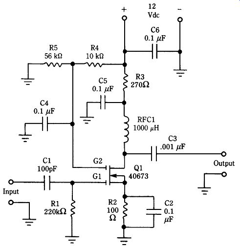
FIG. 5 FR amplifier circuit.
455-kHz AM IF-amplifier test-and-alignment oscillator
The modern superheterodyne AM radio uses a 455-kHz IF amplifier (262.5 kHz is used on AM car radios). FIG. 6 shows a simple signal-generator circuit that can be used to test, troubleshoot, or align the AM IF stage in common radios. The active element is a MPF-102 (or NTE-312) JFET.
As you can see by comparing Fig. 6 to Fig. 2, this circuit is of the basic Hartley oscillator class because it uses a tapped inductor (T1) in the feedback net work. The transformer used for this purpose is a standard 455-kHz IF transformer (Digi-Key Part No. TK-1301, or equivalent). This transformer has a tapped primary that is used to match the low collector impedance of bipolar (PNP or NPN) transistor amplifiers, but the tapped LC tank circuit can be pressed into service as a Hartley oscillator. The secondary of the transformer forms a handy output port to pass a 455 kHz signal to the following buffer stage (see Fig. 5 for a description of this circuit).
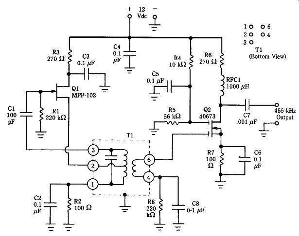
FIG. 6 455-kHz AM IF alignment oscillator.
Signal generator for the AM and shortwave bands
The same general type of circuit can be used for the AM band (530 to 1610 kHz) or for the shortwave bands (1610 kHz to 30 MHz). The version shown in Fig. 7 uses a standard transformer that has a 217-uH inductance in the primary winding.
This particular example uses a Toko coil from Digi-Key (Part No. TK-1903) in con junction with a 365-pF broadcast variable capacitor to cover the AM broadcast band.
For other frequencies:

(Eqn. 1) or if F and L are known but C is unknown:
(Eqn. 2) or if F and C are known but L is unknown:
(Eqn. 3) L _ 1 39.5 F2 C C _ 1 39.5 F2 L F _ 1 2_2LC
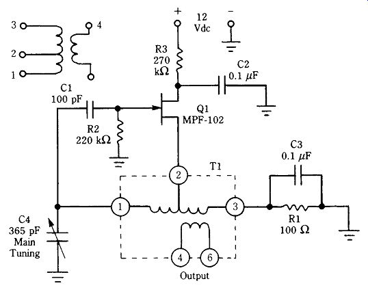
FIG. 7 Variable alignment oscillator.
In all three cases, F is in hertz, C is in farads, and L is in henrys. For frequencies at which there is not an easily available coil, select a toroidal core and wind a coil yourself. In either case, allow about 20 pF for stray capacitances in the circuit (the actual amount might be more or less, depending on the layout).
A VHF voltage-tuned oscillator circuit is shown in Fig. 8A. I've used this circuit at frequencies from 20 to 150 MHz. The circuit uses a feedback capacitor (C2) across the collector-emitter circuit of the transistor. This capacitor is critical, and the circuit probably won't oscillate without it. The tuning network consists of inductor, L1; dc-blocking capacitor, C1; and varactor, D1. Varactors are voltage-variable capacitor diodes. The inductor is wound on either a VHF toroidal coil or an air form about 3 _ 8_ in diameter. If no. 20 or so solid wire is used for L1 then the coil will be self supporting after it is removed from the coil form.
The VHF oscillator of Fig. 8A is tuned with a dc voltage (Vt) applied through a 150-kOhm resistor (R4). This voltage is positive in order to reverse bias D1. A problem with this circuit is that the frequency is a nonlinear function of frequency because of the characteristics of D1. FIG. 8B shows a somewhat more linear version of this same circuit. In this case, the dc-blocking capacitor is replaced with a second varactor diode that is identical to the first. The total capacitance of the combination is half the capacitance of one diode, but the voltage-vs-frequency characteristic is more linear.
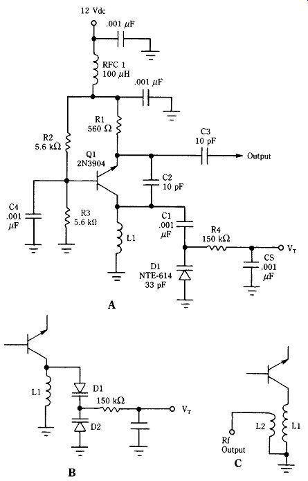
FIG. 8 (A) Varactor tuned VHF variable frequency oscillator, (B) alternate
control circuit, and (C) alternate output circuit.
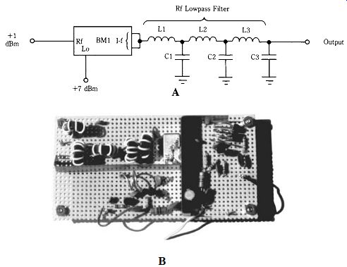
FIG. 9 Balanced mixer with low-pass filter output for mixing two RF sources.
(A) RF low-pass filter connected to balanced mixer; (B) physical implementation.
Both of these circuit variations can be fixed-tuned with a dc voltage, variable tuned through a potentiometer, or swept across a band of frequencies with a sine wave (FM) or sawtooth signal. In the case of the sawtooth, use a 10- to 60-Hz signal.
A variation on the theme is shown in Fig. 8C. Although the output in Fig. 8A is taken from the emitter of the transistor, the variation in Fig. 8C uses a secondary winding over the tuning inductor (L1) to output the signal.
Another variation useful for a wide variety of circuits is shown in Fig. 9A, and an actual example prototyped by me is shown in Fig. 9B. This circuit uses a double balanced mixer (DBM), such as the SRA-1 and related products by Mini-Circuits Laboratories, Inc. One signal is applied to the RF port of the DBM, and the other signal is applied to the LO port of the DBM (note the relative signal levels). The difference frequency is taken across the two shorted IF OUT ports. The low-pass filter is used to remove residual LO or RF signal. I used this scheme to produce a ham-band sweep generator. One oscillator was fixed tuned to 37 MHz then swept with a saw tooth tuning voltage 1 MHz. The other oscillator was tuned to frequencies that would heterodyne the 37-MHz signal to the middle of various HF ham bands. A bank of potentiometers selects the dc bias required to achieve the correct output frequency.
The RF signal generator circuit is generally well-behaved and thus is easy to build and align if proper technique is used. You can be quite successful making these circuits perform the tasks for which they were designed.