AMAZON multi-meters discounts AMAZON oscilloscope discounts
The very low frequencies (VLF) are located between a few kilohertz and around 300 kHz, depending on whose definition is used. For purposes of this section VLF represents the 5- to 100-kHz region. The reason for this seemingly arbitrary designation is that many ham-band and SWL communications receivers operate down to 100 kHz and only a few operate below that limit.
A lot of radio stations are active in the region below 100 kHz. Perhaps the best known station is WWVB on 60 kHz. This station is operated from Colorado by the National Institutes for Standards and Technology (NIST). WWVB is a very accurate time and frequency station and for many purposes is preferred over the high frequency WWV and WWVH transmissions. The U.S. Navy operates submarine communications stations in the VLF region, NSS on 21.4 kHz from Annapolis, Maryland (400 kW) and NAA on 24 kHz from Cutler, Maine (1000 kW) being two most commonly heard. Other stations, in both the United States and abroad, are found throughout the VLF region.
But DX-ing in the VLF band is not all that easy. Besides the fact that propagation doesn't support "skip" the way the 20-m ham band does, huge noise signals are in the VLF region. Two sources seem to predominate. First, the 60-Hz power lines are terrible offenders. Although it might seem counterintuitive that a 60-Hz signal could be of much concern at, for example, 30 kHz, it nonetheless is. The high harmonics are caused by harmonic-laden alternating current from the power lines. In addition, the large amounts of power carried by normal residential power lines makes even the higher harmonics at least strong enough to interfere with sensitive receivers.
The second form of interference is the neighborhood television sets. The horizontal oscillator in TV receivers operates at 15.734 kHz, and it is a pulse. As a result, harmonics from television sets can be found up and down the VLF spectrum. And furthermore, the TV horizontal pulse produces its own "sidebands," so each harmonic actually wipes out a lot of spectrum space on either side of the integer multiple of 15.734 kHz. Listening to VLF allows you to identify the evenings when a popular TV presentation is on the air. As a result of TV interference, it is common to find VLFers listening during daylight hours and during the period between midnight and daybreak.
Amateur scientists use VLF receivers in two different types of activity. Some are active in monitoring solar activity that affects radio propagation. Sudden ionospheric disturbances (SIDs) can be noted by sudden increases in VLF signal levels (Taylor and Stokes, 1991; Taylor, 1993). The SID monitoring activity occurs in the 20- to 30-kHz region, although some articles cite as high as 60 kHz.
The other VLF amateur science activity involves looking for naturally created radio signals called whistlers. These signals are believed to be created by lightning storms and are propagated at long distances. They occur in the 1- to 10-kHz region (Mideke, 1992 and Eggleston, 1993). At least one project under the sponsorship of NASA engaged amateurs to look at whistlers.
Receiver types
Virtually all common designs are used for VLF receivers, except possibly the crystal set. This section covers the superheterodyne, the direct conversion, the tuned radio frequency, and the tuned-input gain block methods. It also includes the use of a converter to translate the VLF bands to the HF bands so that an ordinary ham band or SWL receiver can be used.
Superheterodynes
The "superhet" (FIG. 1) is the basic receiver design used in communications and broadcast receivers. It dates from the 1920s and is the most successful receiver design. In the superhet receiver, the incoming RF signal (at frequency F1) is filtered by a tuned RF-resonant circuit or a bandpass filter then applied to a mixer circuit. In most cases, the RF signal is amplified in an RF amplifier (FIG. 1), but that is not a necessary requirement. The mixer nonlinearly combines F1 with the signal from a lo cal oscillator (at frequency F2) to produce an output spectrum of F3 _ mF1 _ nF2.
In our simplified case, m _ n _ 1, so the output will consist of the two original signals (F1 and F2), the sum signal (F1 _ F2), and the difference signal (F1 _ F2). A filter at the output of the mixer selects either sum or difference signal as F3 and this is called the intermediate frequency (IF). Most of the receiver's gain and selectivity are provided in the IF amplifier. The output of the IF amplifier is fed to a detector that will demodulate the type of signal being received. For an AM signal, a simple envelope detector is used; for CW and SSB, a product detector is used.
In older radios, only the difference signal was used for the IF frequency, but in modern receivers, either the sum or the difference is used. In a VLF receiver, it is possible to use a 10- to 100-kHz RF range, a local oscillator range of 465 to 555 kHz, to produce an IF of 455 kHz (one of the common "traditional" frequencies).
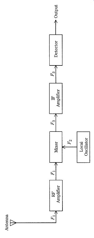
FIG. 1 Block diagram of a superheterodyne receiver.
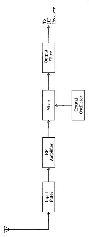
FIG. 2 VLF converter block diagram.
Converters
A subclass of superheterodyne receivers is the converter technique (FIG. 2), in which the VLF band is frequency translated to the high-frequency (HF) bands.
The typical converter circuit is rather simple. An input filter (either bandpass or tuned to a specific frequency) feeds an optional RF amplifier and then a mixer. A fixed-frequency crystal oscillator mixes with the RF signal to produce an output on an IF that is in the ham band or some other shortwave band. For example, to receive 10 to 100 kHz, the input filter (FIG. 2) could be a bandpass filter with _3-dB points at 10 and 100 kHz. The local oscillator could be a 3600-kHz crystal oscillator.
The output filter is a 3610- to 3710-kHz bandpass filter, the output of which is fed to an 80-m ham-band receiver. However, the feedthrough of the 3600-kHz crystal oscillator signal must be reduced to the receiver. A combination of using a double balanced mixer and proper termination of the mixer will generally cure this problem.
Tuned radio frequency (TRF) receivers The TRF receiver (FIG. 3) uses a cascade chain of tuned RF amplifiers (A1, A2, and A3) to amplify the radio signal. The TRF was the first really sensitive design in the early 1920s and was eclipsed by the superhet in popular commercial receivers.
But in the VLF range, the TRF is still popular-especially among homebrewers. A problem with the TRF receiver is the possibility of unwanted oscillations, which are common in tuned triode devices, such as NPN bipolar transistors.
Peter Taylor's column in the Spring 1993 Communications Quarterly gave de tails of a 20- to 30-kHz TRF receiver for SID monitoring that was designed by Art Stokes ( Taylor, 1993).
Tuned gain block (TGB) receivers
The TGB receiver (FIG. 4A) is basically a variant of the TRF receiver, except that the tuning circuits are all up front, ahead of the gain. Two benefits are realized.
First, the oscillation problem of conventional TRF receivers is avoided because the gain block is untuned. Second, the tuning up front eradicates much of the unwanted noise prior to it being amplified. The actual circuit is shown in FIG. 4B. The three amplifier stages consist of high-gain NPN transistors, such as the 2N4416. Tuning is accomplished by connecting a fixed or variable capacitor across input coil L1. The output circuit consists of a voltage doubler detector (D1/D2) and an integrator capacitor (C10). This combination converts the output of the receiver to a dc voltage used to detect the signal. This dc level is recorded on a 1-mA recorder or is input to a computer via an A/D converter. If the latter approach is taken, connect a 10-k_ resistor across capacitor C10 to convert the output current to an output voltage.
Tuning circuit problems
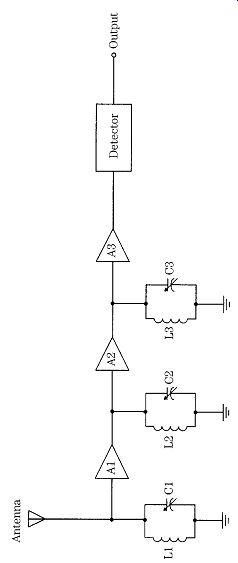
FIG. 3 Tuned radio frequency (TRF) receiver.
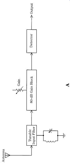
FIG. 4 (A) Block diagram of the VLF SID hunter's receiver and (B) schematic
diagram of circuit.
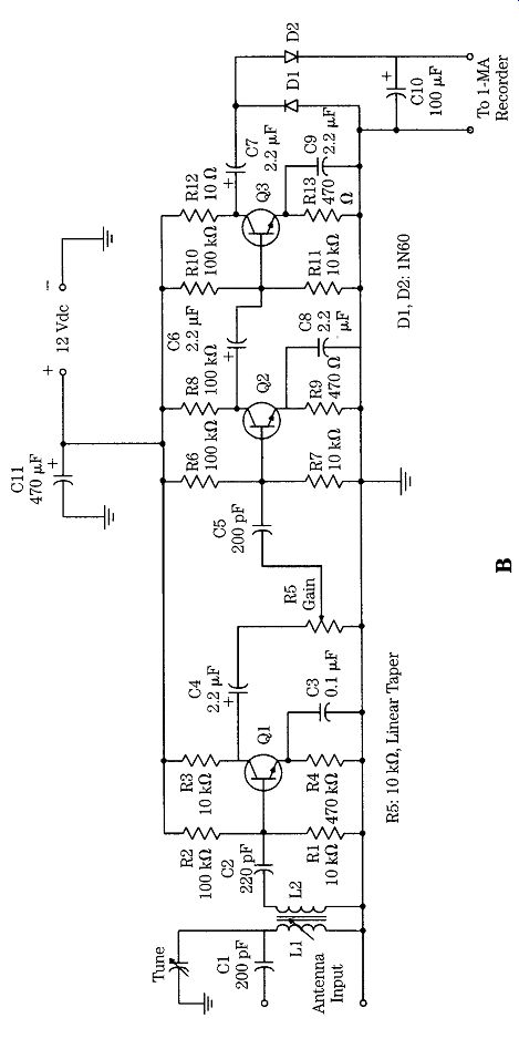
FIG. 4 Continued.
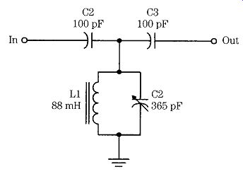
FIG. 5 Alternate tuning circuit.
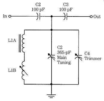
FIG. 6 Tuning circuit using one fixed and one variable inductor.
The principal problem to solve in designing and building VLF receivers is the tuning circuits. The capacitance and inductance values tend to be rather large. If you want to use a standard "broadcast variable" capacitor, which is typically 10 to 365 pF in capacitance value, then a 20- to 30-kHz receiver needs an inductor in the 88-mH range. The calculated value of capacitance needed to resonate 88 mH at 20 to 30 kHz is 720 pF. The reason why a smaller variable capacitance is used is that the distributed capacitance of large coils, such as 88 mH, is typically quite large.
The Stokes TGB receiver used a tuned circuit (FIG. 4B). Originally, a J. W. Miller 6319 inductor was used, but these apparently are no longer available. The 1993 TRF design used 88-mH "telephone" toroid inductors. The TRF circuit (FIG. 5) used the 88-mH inductor paralleled by a 365-pF variable capacitor and isolated it for dc by a pair of 100-pF capacitors (C2 and C3 in FIG. 5).
A problem with the simple circuit of FIG. 5 is that it is not easy to adjust the tuning range (i.e., the receiver cannot be aligned). A variant on the theme, shown in FIG. 6, adds a small variable "trimmer" capacitor (C4) shunted across the main tuning capacitor (C1), and a trimmer inductor (L1B) is in series with the main fixed inductor (L1A). It would be nice to obtain a single inductor that has the tuning range, but they are hard to obtain these days. As shown, the circuit can be adjusted over about 10% of the inductance range. In one version, a 100-ohmH fixed inductor was connected in series with a 56-uH variable inductor.
When using the TGB design, all of the tuning is done ahead of the gain block.
This poses certain problems for the tuning circuit-especially if more than one tuned LC circuit is desired for selectivity purposes. Figures 7 and 8 show several methods for combining LC-tuned circuits; both of them fall into the "mutual reactance" method but with different approaches.
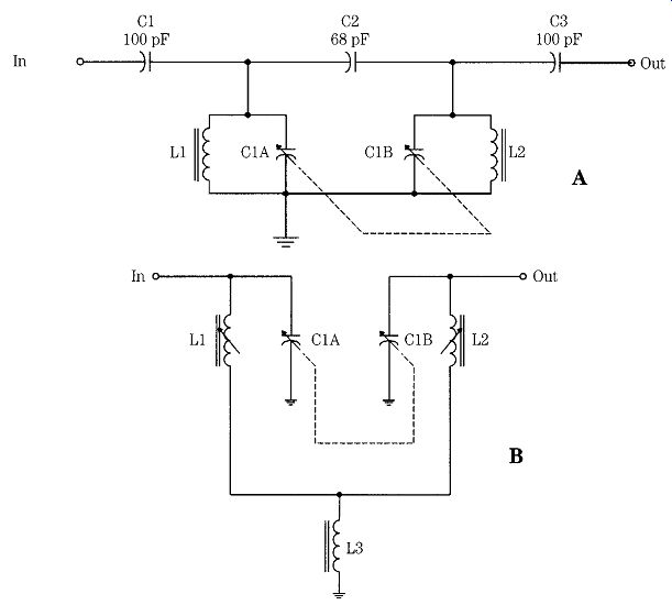
FIG. 7 Mutual reactance coupling: (A) capacitance and (B) inductance.
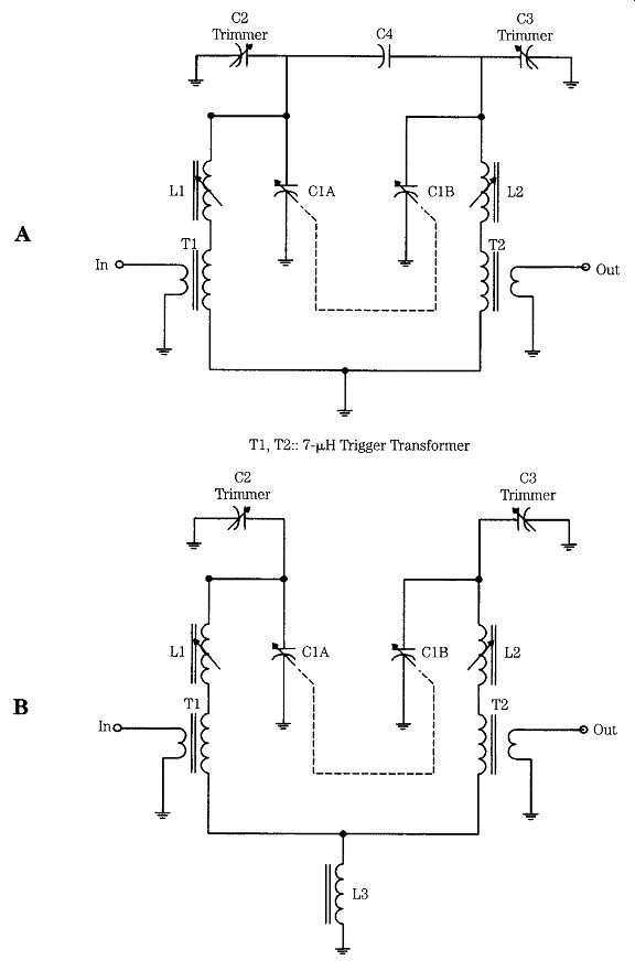
FIG. 8 (A) Using a flash-tube trigger transformer as a circuit element and
(B) using custom wound coils.
In FIG. 7A, a small capacitance (33 to 120 pF) is used to couple the two LC resonant circuits (L1/C1A and L2/C1B). In FIG. 7B, a common inductor (L3) is used for the same purpose. Experiments show that a value of 150 to 700 _H is needed for L3. The ARRL Handbook for Radio Amateurs (all recent editions) provides details on selecting values for the components in these circuits.
A different approach to the design of receiver front ends is shown in FIG. 8.
One of the problems in VLF receiver design is providing low-impedance link coupling into and out of the LC tank circuit. Large inductance coils are not very often avail able with low impedance transformer windings. For example, in the Digi-Key catalog, the largest coil with such a winding is a 220-uH unit, which is intended for the AM broadcast band. The solution was the series inductor method (FIG. 6). In this case, however, a 56-mH variable inductor was connected in series with a xenon flash tube trigger transformer. The version selected was intended to fire a 6000-V fast rise-time pulse into a xenon flash tube, and it has a nominal inductance of 6.96 mH +-20%. The measured inductance was 7.1 uH, and the self-resonance frequency was 140 kHz. Without the trimmer capacitors, the tuning range was 30 to 60 kHz when a 2 _ 380-pF variable capacitor was used. Adding a 600-pF trimmer across each section of the main tuning capacitor reduced the tuning range to 20 to 30 kHz. The approach in FIG. 8A uses a capacitor (C4) for the mutual reactance, and in FIG. 8B, an inductor is used (L3).
The trigger transformers are widely available from mail-order sources. However, I ordered several from an English source, Maplin Electronics (P.O. Box 3, Rayleigh, Essex SS6 8LR, England). They have variable capacitors, coil forms, and a number of other things of interest to amateur radio constructors. The U.S. credit cards accepted include VISA and American Express and the currency exchange is automatic.
Another alternative, although I've not tested it, is to use pulse transformers. Un fortunately, these transformers typically have limited turns ratios (2:1:1).
A VLF receiver project
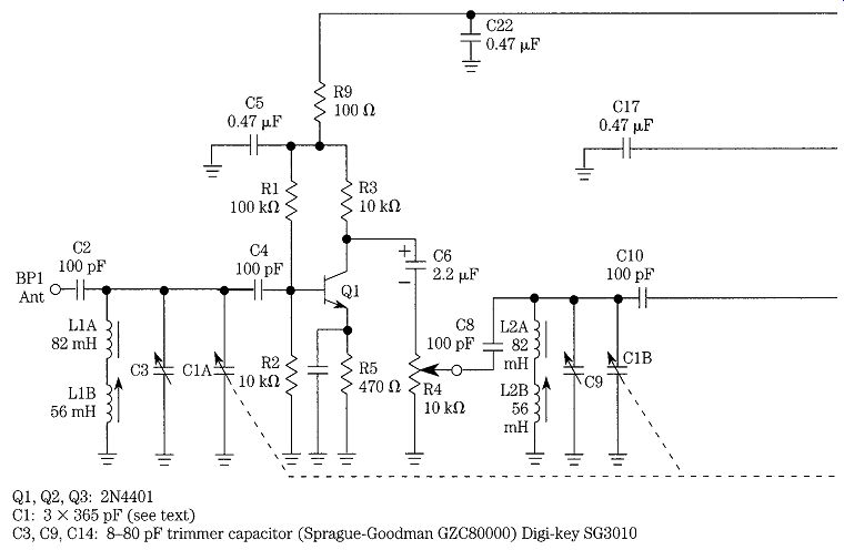
FIG. 9 Schematic of the VLF receiver project.
The circuit for a modified VLF receiver is shown in FIG. 9. It uses the same basic circuit as the Stokes design but with these modified tuning circuits. The 82-mH fixed inductors (L1A, L2A, and L3A) are the Toko 181LY-823J, which are available from Digi-Key ( P.O. Box 677, Thief River Falls, MN 56701-0677; 1-800-344-4539) under catalog number TK-4424. The 56-mH variable inductors are Toko CLNS-T1039Z, available under Digi-Key TK-1724. An additional degree of adjustment is provided by using an 8- to 80-pF trimmer capacitor across each section of the 3 _ 365-pF variable main tuning capacitor. These capacitors are Sprague-Goodman GZC8000 units (Digi-Key SG3010).
The output circuit for this receiver reflects the fact that it is a SID monitor receiver. The detector is a voltage doubler (D1/D2) made from germanium diodes. The original diodes specified were 1N34 but 1N60s work well also. If you cannot find these diodes (RadioShack and Jim-Pak sells them) then try using replacements from the "universal" service shop replacement lines, such as SK, NTE, and ECG. The NTE-109s and ECG-109s will work well. The output of the detector is heavily integrated by a 470-uF electrolytic capacitor. The output as shown is designed to feed a current-input recorder or a microammeter. If a voltage output is desired then connect a resistor (3.3 to 10 kO) across capacitor C19.
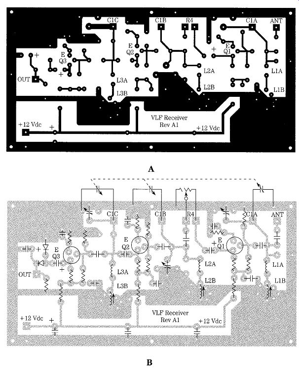
FIG. 10 PC board for the VLF receiver. (A) PCB pattern for VLF receiver; (B)
parts layout.
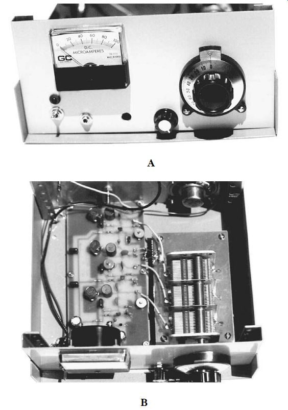
FIG. 11 Completed receiver.
Fig. 10A shows a printed circuit board for use with this circuit, and FIG. 10B is the components' placement "roadmap." The board is designed for these specific components (FIG. 9). Variations on the theme can be accommodated by using different value inductors from the same Toko series (see Digi-Key catalog; the L1-series coils are Toko size 10RB and the L2-series coils are size 10PA). Also, if you don't want to use two coils in each tuning circuit, then short out the holes for L1 positions and use a coil in the L2 positions with the required inductance.
The final receiver is shown in FIG. 11. A front-panel view is in FIG. 11A, and an internal view is shown in FIG. 11B. The tuning capacitor was a three- section model purchased from Antique Electronic Supply, Tempe, AZ. Although I first thought it was a 3 _ 365-pF unit, it measured at 550 pF (which is better for VLF anyway). A 2_ vernier dial (Ocean State Electronics, P.O. Box 1458, Westerly, RI 02891; 1-800-866-6626) was used to drive the variable capacitor (notice: Ocean State also sells multi section variable capacitors). The final receiver tuned from 16.5 to 31 kHz.
A later VLF receiver design by Stokes used the gyrator concept to simulate the inductance. Recall that the inductance is the hardest problem in the design of VLF receivers. A gyrator is an operational amplifier circuit (A1 and A2 in FIG. 11) that acts as if it were an inductor. The value of the inductance is set by the values of the resistors and of capacitor C3. Op amp A3 is a noninverting follower with a gain of 100 and provides half of the RF gain and most of the dc gain for the circuit.
After being amplified in A3, the signal is split into two paths. The original Stokes design went directly to a precision rectifier/integrator, but I needed an RF output as well. When I built the original design, I found that the RF output waveform was distorted by the action of the precision rectifier. In order to overcome that problem, I changed the design to that of FIG. 11. Amplifier A5 buffers the input of the precision rectifier (A6) to isolate it from the RF output circuit. The RF output could be taken directly from the output of A3, but I opted instead to use a gain-of-2 noninverting follower (A4) to buffer the RF output and provide some additional gain.
This receiver is a single-channel model and will tune the 17- to 30-kHz range preferred by SID hunters. Because it is single-channel, I used 15-turn PC-mounted trimmer potentiometers for R3 and R7. The receiver was built into a SESCOM SB-7 RF box.
The operational amplifiers used in this circuit must have a gain-bandwidth product high enough to support amplification at the frequencies involved (741-family op amps won't cut it). The original Stokes design used four op amps, so he used the 4136 device. The 4136 is a quad op amp. Other alternatives include the 5534, CA 3140, or CA-3160 (all single op amps) or the CA-3240 (dual op amp).
The dc power supply is extremely important in this circuit. The circuit will operate from any potential over _9 to _12 Vdc. It is critical that the dc power supply lines be well-bypassed. In FIG. 12, only a single op amp is shown in the power connections inset but it serves as a reference for all stages. Each package (whether quad, dual, or single op amp) will have V_ and V_ terminals. Each of these terminals must be bypassed to ground through 0.1-uF capacitors. These capacitors should be placed as close to the body of the op amp as possible (otherwise oscillation might occur). The V_ and V_ lines should be bypassed with electrolytic capacitors (be mindful of polarity!) in the 470- to 2000-uF range.
A multiband variant is shown in FIG. 13. This receiver is identical to the version of FIG. 12, except that the band-set capacitor (C3) is replaced by a bank of four switched capacitors.
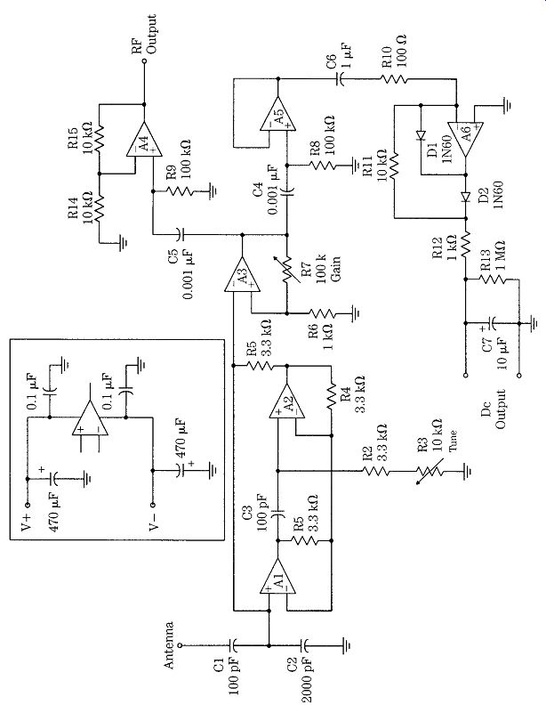
FIG. 12 VLF receiver using "virtual inductor" gyrator circuit (after
a design by Art Stokes).
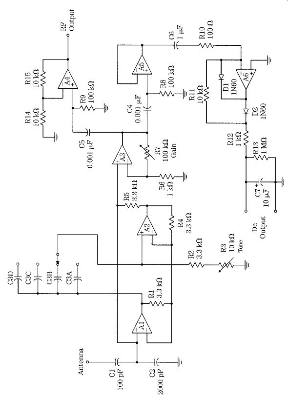
FIG. 13 Multiband VLF receiver.
The inductance simulated by the gyrator is calculated from:

(Eqn. 1)
The inductance required for any given frequency (in hertz) is calculated from:
(Eqn. 2)
L_H _ 1 39.5 F2 HZ CuF
L_H _ C3uF _ R5 _ 1R2 _ R32.
The use of a VLF converter is shown in FIG. 14A, and an actual converter circuit is shown in FIG. 14B. The converter is placed in the signal path between the antenna and the antenna input of the receiver. The converter circuit in FIG. 14B is based on the NE-602 chip. The oscillator section operates at 4000 kHz (i.e., 4 MHz), and the input is tunable over whatever range needed in the range 10 to 500 kHz. Tuning is accomplished by resonating the secondary winding of T1 with capacitor C3. The difference frequency will be either 3500 to 4000 kHz (difference IF), or 4000 to 4500 (sum IF), so the VLF signals will appear in either range (the sense of the tuning will be low to high if the sum IF is selected).
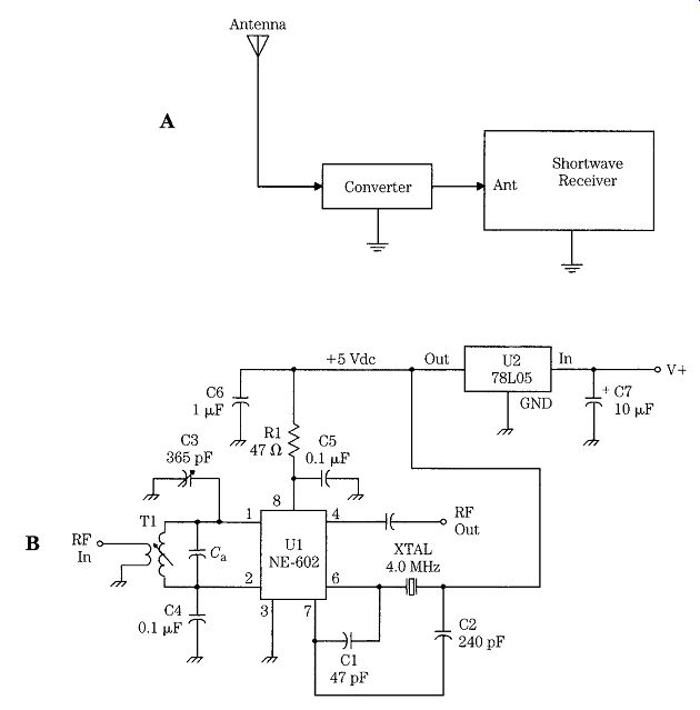
FIG. 14 (A) Converter connection to SW receiver and (B) typical VLF converter
circuit.
References and notes:
Eggleston, G. (1993). "The Sky Chorus," Popular Electronics, July, p. 46.
Mideke, M. (1992). "Listening to Nature's Radio," Science Probe!, July, p. 87.
Pine, B. "High School Support for Space Physics Research." Unpublished paper sent to participants in Project INSPIRE.
Taylor, P., and Stokes, A. (1991). "Recording Solar Flares Indirectly." Communications Quarterly, Summer, p. 29.
Taylor, P. (1993). "The Solar Spectrum: Update on the VLF Receiver." Communications Quarterly, Spring, p. 51.