AMAZON multi-meters discounts AMAZON oscilloscope discounts
OIn radio-frequency electronics, a mixer is a nonlinear circuit or device that permits frequency conversion by the process of heterodyning. Mixers are used in the "front end" of the most common form of radio, the superheterodyne (regardless of wave band), in certain electronic instruments and in certain measurement schemes (receiver dynamic range, oscillator phase noise, etc.).
The block diagram for a basic mixer system is shown in Fig. 20-1; this diagram is generic in form, but it also represents the front end of superheterodyne radio receivers. The mixer has three ports: F1 receives a low-level signal and would correspond to the RF input from the aerial in radio receivers, F2 is a high-level signal and corresponds to the local oscillator (LO) in superhet radios; and F3 is the resultant mixer product (corresponding to the intermediate frequency or "IF" in superhet radios). These frequencies are related by:

(20-1)
... where...
F1, F2, and F3 are as described
m and n are counting numbers (zero plus integers 0, 1, 2, 3, . . .).
In any given system, m and n can be zero, or any integer, but in practical circuits, it is common to consider only the first-, second-, and third-order products. For sake of simplicity, let's consider a first-order circuit (m =n= 1). Such a mixer would output four frequencies: F1, F2, F3a = F1 + F2, and F3b = F1 - F2. In terms of a radio receiver, these frequencies represent the RF input signal, the local oscillator signal, the sum IF, and the difference IF. In radios, it is common practice to select either sum or difference IF by filtering and rejecting all others.
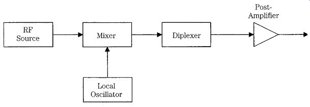
20-1 Block diagram of a mixer circuit.
There are a number of different types of mixer circuits, but only a few different classes: single-ended, singly balanced (or simply "balanced"), and doubly balanced.
Most low-cost superheterodyne radio receivers use single-ended mixers, although a few of the more costly "communications receiver" models use singly or doubly balanced mixers for improved performance. This section focuses on the doubly balanced mixer (DBM) because it offers superior performance over the other forms but is not as well known in electronic hobby circles.
One of the advantages of the DBM over the other forms of mixer is that it sup presses F1 and F2 components of the output signal, passing only the sum and difference signals. In a radio receiver using a DBM, the IF filtering and amplifier would only have to contend with sum and difference IF frequencies and not bother with the LO and RF signals. This effect is seen in DBM specifications as the port-to-port isolation figure, which can reach 30 to 60 dB, depending on the DBM model.
A diplexer stage is shown in Fig. 20-1 and is used to absorb unwanted mixer products and pass desired frequencies. A postamplifier stage is typically included because the insertion loss of most passive DBMs is considerable ( 5 to 12 dB). The purpose of the amplifier is to make up for the loss of signal level in the mixing process. Some active DBMs, incidentally, have a conversion gain figure, not a loss.
For example, the popular Signetics NE-602 device offers 20 dB of conversion gain (Carr, 1992).
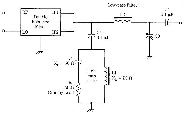
20-2 Diplexer circuit.
Diplexer circuits
The RF mixer is like most RF circuits in that it wants to be terminated in its characteristic impedance. Otherwise, a standing-wave ratio (SWR) problem will result, causing signal loss and other problems. In addition, certain passive DBMs will not work well if improperly terminated. A number of different diplexer circuits are known, but two of the most popular are shown in Figs. 20-2 and 20-3.
A diplexer has two jobs: (1) it absorbs undesired mixer output signals so that they are not reflected back into the mixer and (2) it transmits desired signals to the output. In Fig. 20-2, these goals are met with two different LC networks; a high-pass filter and a low-pass filter. The assumption in this circuit is that the difference IF is desired so a high-pass filter with a cutoff above the difference IF is used to shunt the sum IF (plus and LO and RF signals that survived the DBM process) to a dummy load (R1). The dummy load shown in Fig. 20-2 is set to 50-ohm because that is the most common system impedance for RF circuits (in practice, a 51-_ resistor might be used). The dummy-load resistor can be a 1/4-W unit in most low-level cases, but regardless of power level, it must be a noninductive type (e.g., carbon composition or metal film).
The inductance (L1) and capacitance (C1) values in the high-pass filter are de signed to have a 50-ohm reactance at the IF frequency. These values can be calculated from:
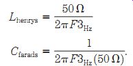
(20-2)

(20-3)
The low-pass filter transmits the desired difference IF frequency to the output, rejecting everything else. Like the high-pass filter, the L and C elements of this filter are designed to have reactances of 50-ohm at the difference IF frequency.
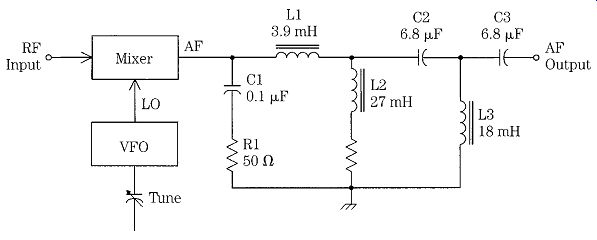
I built a sweep generator to facilitate a high-performance AM band (540 to 1700 kHz) receiver that I designed. The sweeper circuit is a varactor-tuned VCO that is driven with a 45-Hz sawtooth wave. The swept oscillator is heterodyned against a 14-MHz crystal oscillator, producing difference frequencies that can be tuned to either 455 kHz (my selected IF) or any frequency in the AM band. My diplexer unit consists of two 3000-kHz Butterworth filters, one high-pass and the other low-pass; each filter consists of five reactance elements. The high-pass filter was terminated in a 50-ohm dummy load made by paralleling two 100-ohm metal film resistors (that were hand-selected for the correct value). The low-pass filter was terminated in a postamplifier with a 50-ohm input impedance.
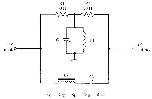
20-3 Alternate diplexer.
20-4 Diplexer for direct-conversion receiver.
Another popular diplexer circuit is shown in Fig. 20-3. This circuit consists of a parallel-resonant 50-ohm tank circuit (C1/L1) and a series-resonant 50-ohm tank circuit (C2/L2). The series-resonant circuit passes its resonant frequency while rejecting all others because its impedance is low at resonance and high at other frequencies. Alternatively, the parallel-resonant tank circuit offers a high impedance to its resonant frequency and a low impedance to all other frequencies. Because C1/L1 are shunted across the signal line, it will short out all but the resonant frequency.
In direct-conversion receivers, a mixer is used to down convert CW and SSB signals directly to audio by setting F2 close to F1, without using an IF amplifier chain. In those receivers, it is common practice to build a diplexer similar to Fig. 20-4. Capacitor C1 passes high frequencies (which are RF), and they are absorbed in a 50-ohm dummy load. The low-frequency audio signals (300 to 3000 Hz) are passed by a 50-ohm low-pass filter consisting of L1, L2, L3, R2, and C2.
JFET and MOSFET doubly balanced mixer circuits
20-5 JFET DBM circuit.
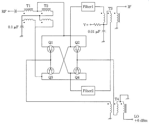
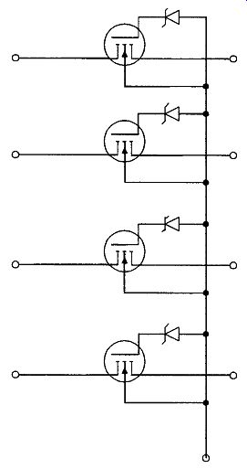
Junction field-effect transistors (JFETs) and metal-oxide semiconductor transistors (MOSFETs) can be arranged in a ring circuit that provides good doubly balanced mixer operation. Figure 20-5 shows a circuit that is based on JFET devices.
Although discrete JFETs such as a MPF-102 or its equivalent can be used in this circuit with success, performance is generally better if the devices are matched or are part of a single IC device (e.g., the U350 IC). The circuit is capable of better than 30-dB port-to-port isolation over an octave (2:1) frequency change.
The inputs and output of this circuit are based on broadband RF transformers.
These transformers are bifilar and trifilar wound on toroidal cores. The input circuit consists of two bifilar-wound impedance transformers (T1 and T2). The LO and out put circuits are trifilar-wound RF transformers. Part of the output circuit includes a pair of low-pass filters that also transform the 1.5- to 2-k ohm impedance of the JFET devices to 50-ohm . As a result of the needed impedance transformation, the filters must be designed with different Rin and Rout characteristics, and that complicates the use of loop-up tables (which would be permitted if the input and output resistances were equal).
Figure 20-6 shows an IC DBM that is based on MOSFET transistors. This device was first introduced as the Siliconix Si8901, but they no longer make it. Today, the same device is made by Calogic Corporation [ 237 Whitney Place, Fremont, CA 94539, USA; phones: 510-656-2900 (voice) and 510-651-3026 (fax)] under the part number SD8901. The SD8901 comes in a seven-pin metal can package. The specifications data sheet for the SD8901 claims that it provides as much as a 10-dBm improvement in third-order intercept point over the U350 JFET design or the diode-ring DBM.
20-6 Si-8901 MOSFET DBM.
20-7 Connection of the 8901 mixer.
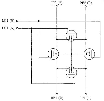
A basic circuit for the SD8901 is shown in Fig. 20-7. The input and output terminals are connected to center-tapped, 4:1 impedance ratio RF transformers. Although these transformers can be homemade (using toroidal cores), the Mini-Circuits type T4-1 transformers were used successfully in an amateur radio construction project (Makhinson, 1993). As was true in other DBM circuits, a diplexer is used at the out put of the SD8901 circuit.
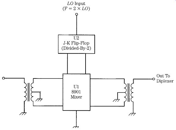
The local oscillator inputs are driven in push-pull by fast-rise-time square waves. This requirement can be met by generating a pair of complementary square waves from the same source. One circuit uses a pair of high-speed TTL J-K flip-flops connected with their clock inputs in parallel, driven from a variable-frequency oscillator that operated at twice the required LO frequency. The complementary requirement was met by using the Q-output of one J-K flip-flop and the NOT-Q output of its parallel twin.
The SD8901 device is capable of very good performance-especially in the dynamic range that is achievable. In the design by Makhinson (cited previously), a _35-dBm third-order intercept point was achieved, along with a _16-dBm 1-dB out put compression point and a 1-dB output blocking desensitization of _15 dBm. Insertion loss was measured at 7 dB.
One problem with the SD8901 device is its general unavailability to amateur and hobbyist builders. Although low in cost, Calogic has a minimum order quantity of 100 and that makes it a little too rich for most hobbyists to consider. A compromise that also works well is the MOS electronic switch IC devices on the market from several companies, including Calogic. Figure 20-8 shows a typical MOS switch, and it is easy to see how it can be wired into a circuit, such as Fig. 20-7. At least one top-of-the-line amateur radio transceiver uses a quad MOS switch for the DBM in the receiver. It would be interesting to see how well low-cost MOS switches (such as the CMOS 4066) would work. I've seen that chip work well as a doubly balanced phase-sensitive detector in medical blood-pressure amplifiers, and those circuits are closely related to the DBM.
20-8 Quad MOSFET switch.
Doubly balanced diode mixer circuits
One of the easiest doubly balanced circuits, whether homebrew or commercial, is the circuit of Fig. 20-9. This circuit uses a diode ring mixer and balanced input, output, and LO ports. It is capable of 30 to 60 dB of port-to-port isolation yet is reasonably well-behaved in practical circuits. DBMs such as Fig. 20-9 have been used by electronic hobbyists and radio amateurs in a wide variety of projects from direct conversion receivers to single-sideband transmitters to high-performance shortwave receivers. With proper design, a single DBM can be made to operate over an extremely wide frequency range; several models claim operation from 1 to 500 MHz, with IF outputs from dc to 500 MHz.
The diodes (D1 through D4) can be ordinary silicon VHF/UHF diodes, such as 1N914 or 1N4148. However, superior performance is expected when Schottky hot carrier diodes, such as 1N5820 through 1N5822, are used instead. Whatever diode is selected, all four devices should be matched. The best matching of silicon diodes is achieved by comparison on a curve tracer, but failing that, there should at least be a matched forward/reverse resistance reading. Schottky hot-carrier diodes can be matched by ensuring that the selected diodes have the same forward voltage drop when biased to a forward current of 5 to 10 mA.
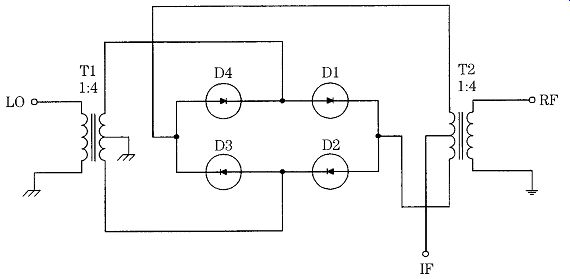
20-9 Diode DBM.
20-10 SBL/SBA mixer circuit.
20-11 SBL/SBA package.
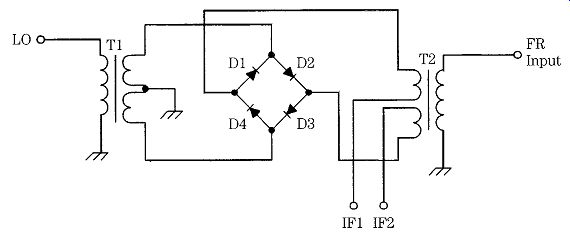
Figure 20-10 shows the internal circuitry for a very popular commercial diode DBM device, the Mini-Circuits SRA-1 and SBL-1 series. A typical SRA/SBL package is shown in Fig. 20-11. These devices offer good performance and are widely avail able to hobbyist and radio amateur builders. Some parts houses sell them at retail, as does Mini-Circuits [P.O. Box 166, Brooklyn, NY, 11235, USA: phone 714-934-4500]. In the U.K, contact Dale Electronics Ltd., Camberley, Surrey, 025 28 35094. In the Netherlands, contact "Colmex" B.V., 8050 AA Hattem, Holland, (0) 5206-41214/ 41217. I don't know the amount of their minimum order, but I've had Mini-Circuits in the USA respond to $25 orders on several occasions--which is certainly more reasonable than other companies.
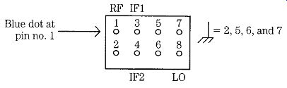
The packages for the SRA/SBL devices are similar, being on the order of 20 mm long with 5-mm pin spacing. The principal difference between the packages for SRA and SBL devices is the height. In these packages, pin 1 is denoted by a blue bead insulator around the pin. Other pins are connected to the case or have a green (or other color) bead insulator. Also, the "MCL" logo on the top can be used to locate pin 1: the "M" of the logo is directly over pin 1. Table 20-1 shows the characteristics of several DBMs in the SRA and SBL series, while Table 20-2 shows the pin assignments for the same devices.
In the standard series of devices, the RF input can accommodate signals up to _1 dBm (1.26 mW), although the LO input must see a _7 dBm (5 mW) signal level for proper operation. Given the 50-ohm input impedance of all ports of the SRA/SBL devices, the RF signal level must be kept below 700 mV p-p, while the LO wants to see 1400 mV p-p. It is essential that the LO level be maintained across the band of interest or else the mixing operation will suffer. Although the device will work down to _5 dBm, a great increase in spurious output and less port-to-port isolation are found. Spectrum analyzer plots of the output signal at low LO drive levels show considerable second- and third-order distortion products.
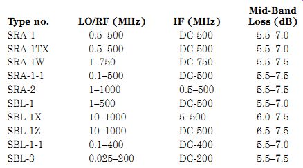
Table 20-1. Mixer specifications
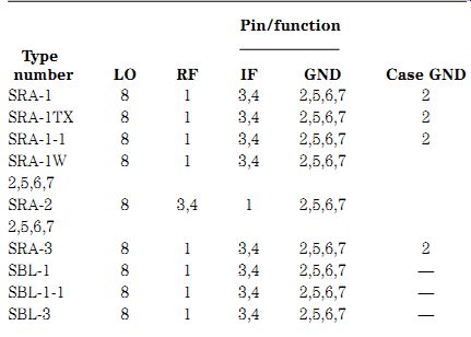
Table 20-2. Mixer pin-outs
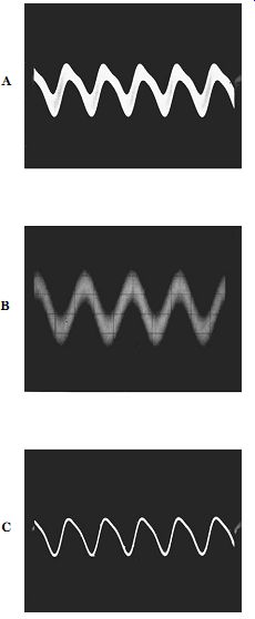
20-12 Waveforms of mixer: (A) improper termination, (B) with portion of
diplexer removed, and (C) properly terminated DBM.
Notice the IF output of the SRA/SBL devices. Although some models in the series use a single IF output pin, most of these devices use two pins (3 and 4), and these must be connected together externally for the device to work.
As is true with most DBMs and all diode-ring DBM circuits, the SRA/SBL devices are sensitive to the load impedance at the IF output. Good mixing, and freedom from the LO/RF feedthrough problem, occurs when the mixer "looks" into a low VSWR load. For this reason, a good diplexer circuit is required at the output. In experiments, I've found that unterminated SBL-1-1 mixers produce nearly linear mixing when not properly terminated-and that's not desirable in a frequency converter.
20-13 Output termination for SBL/SBA.
The effects of the termination impedance on the operation of the diode DBM circuit are shown in Fig. 20-12. The oscilloscope photo in Fig. 20-12A shows the mixer output directly at pins 3 and 4 of an SBL-1-1. Notice that it is a complex waveform of mixed signals and reflects the fact that the mixer is not properly terminated. The waveform at Fig. 20-12B was taken at the output of the low-pass filter when the high pass filter and its associated dummy load was disconnected. At Fig. 20-12C is the resultant when properly matched high-pass (and dummy load) and low-pass filters were in operation. The waveform was a nearly clean sine wave of 455 kHz. Another waveform, not shown, was obtained when there was no high-pass filter, but the DBM was terminated in a resistance matched to its characteristic impedance and a low pass filter. It was a distorted sine wave, and it reflected that other products were present in the output signal.
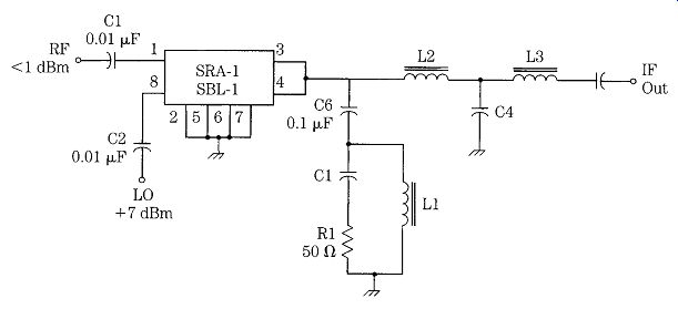
Figure 20-13 shows a typical SRA/SBL circuit: RF drive (__1 dBm) is applied to pin 1, and the _7 dBm LO signal is applied to pin 8. The IF signal is output through pins 3 and 4, which are strapped together. All other pins (2, 5, 6, and 7) are grounded.
The diplexer circuit consists of a high-pass filter (C1/L1) that is terminated in a 50-ohm dummy load for the unwanted frequencies, and a low-pass filter (L2/L3 /C4) for the desired frequencies. All capacitors and inductors are selected to have a reactance of 50-ohm at the IF frequency.
Sometimes 1-dB resistor _-pad attenuators are used at the inputs and the IF output of the DBM. In some cases, the input attenuators are needed to prevent over load of the DBM (overload causes spurious product frequencies to be generated and might cause destruction of the device). In other cases, the circuit designer is at tempting to "swamp out" the effects of source or load-impedance variations. Al though this method works, it is better to design the circuit to be insensitive to such fluctuations rather than to use a swamping attenuator. The reason is that the resistive attenuator causes a signal loss and adds to the noise generated in the circuit (no resistor can be totally noise-free). A good alternative is to use a stable amplifier with 50-ohm input and output impedances, and that is not itself sensitive to impedance variation to isolate the DBM.
Mini-Circuits devices related to the SRA-1 and SBL-1 incorporate MAR-x series MMIC amplifiers internal to the DBM. One series of devices places the amplifier in the LO circuit so that much lower levels of LO signal will provide proper mixing. An other series places the amplifier in the IF output port. This amplifier accomplishes two things: it makes up for the inherent loss of the mixer and it provides greater freedom from load variations that can affect the regular SRA/SBL devices.
Bipolar transconductance cell DBMs Active mixers made from bipolar silicon transistors formed into Gilbert transconductance cell circuits are also easily available. Perhaps the two most common de vices are the Signetics NE-602 device and the LM-1496 device (Maplins catalog no. QH47B, p. 463 in 1993 edition) [Maplins, P.O. Box 3, Rayleigh, Essex SS6 8LR, Eng land; phones (0702) 554161 (credit card orders) and (0702) 552911 (inquiries)].
The NE-602 device is shown in block diagram form in Fig. 20-14A and in partial circuit form in Fig. 20-14B. It offers 20 dB of conversion gain, good sensitivity, and good noise figure, but suffers a bit in the third-order intercept (which is only 15 dBm referenced to a matched input). Consequently, it is recommended that the LO signal be restricted to 200 mV, and the RF input be restricted to 70 mV, into the 1500-ohm input impedances of these terminals.
The LM-1496 device is shown in Figs. 20-15A through 20-15C. Figure 20-15A shows the internal circuitry, and Figs. 20-15B and 15C show the DIP and metal can packages, respectively. Pins 7 and 8 form the local oscillator (or "carrier" in communications terminology) input, and pins 1 and 4 form the RF input. These push-pull inputs are also sometimes labeled "high-level signal" (pins 7 and 8) and "low-level signal" (pins 1 and 4) inputs. Dc bias (pin 5) and gain adjustment (pins 2 and 3) are also provided.
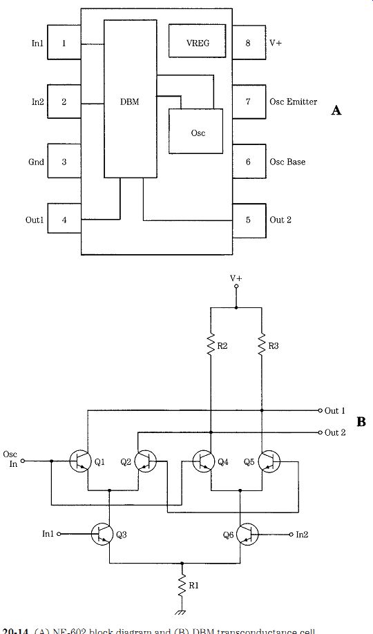
20-14 (A) NE-602 block diagram and (B) DBM transconductance cell.
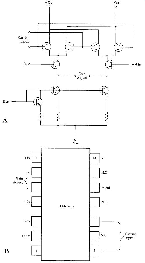
20-15 LM-1496 DBM: (A) internal circuit, (B) 14-pin DIP p (C) 10-pin metal
can package.
20-15 Continued.
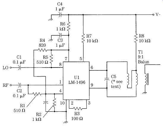
20-16 Mixer circuit based on LM-1496.
Figure 20-16 shows the basic LM-1496 mixer circuit in which the RF and carrier inputs are connected in the single-ended configuration. The respective signals are applied to the input pins through dc-blocking capacitors C1 and C2; the alternate pin inputs in both cases are bypassed to ground through capacitors C3 and C4.
The output network consists of a 9:1 broadband RF transformer that combines the two outputs and reduces their impedance to 50-ohm . The primary of the trans former is resonated to the IF frequency by capacitor C5.
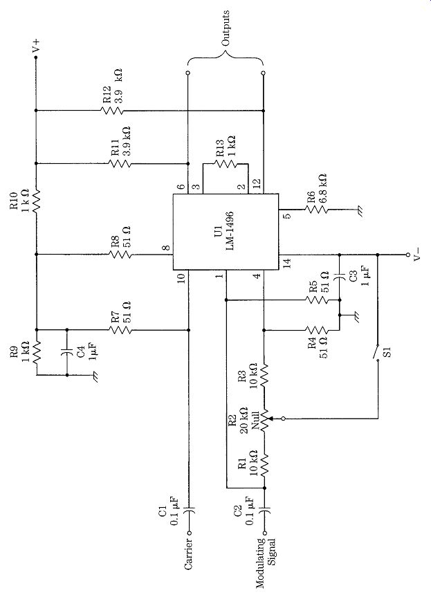
Figure 20-17 shows a circuit that uses the LM-1496 device to generate double sideband suppressed-carrier (DSBSC) signals. When followed by a 2.5- to 3-kHz bandpass filter that is offset from the IF frequency, this circuit will also generate single-sideband (SSB) signals. Commonly, a crystal oscillator will generate the carrier signal (Vc), and the audio stages produce the modulating signal (Vm) from an audio oscillator or microphone input stage. I once saw a circuit that is very similar to this one in a signal generator/test set used to service both amateur radio and marine HF-SSB radio transceivers. It was the signal source to test the receiver sections of the transceivers. The carrier was set to 9 MHz, and both lower sideband (LSB) and upper sideband (USB) KVG crystal filters were used to select the desired sideband.
An alternate scheme that is cheaper uses a single 9-MHz crystal filter, but two different crystals at frequencies either side of the crystal passband. One crystal generates the USB signal, and the other generates the LSB signal.
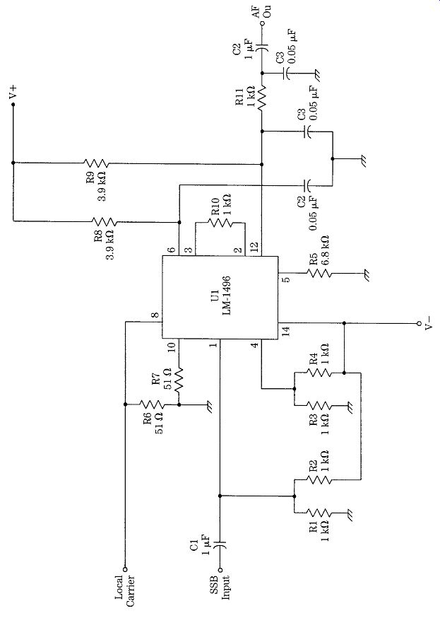
For single sideband to be useful, it has to be demodulated to recover the audio modulation. The circuit of Fig. 20-18 will do that job nicely. It uses a LM-1496 DBM as a product detector. This type of detector works on CW, SSB, and DSB signals (all three require a local oscillator injection signal) and produces the audio resultant from heterodyning the local carrier signal against the SSB IF signal in the receiver.
All SSB receivers use some form of product detector at the end of the IF chain, and many of them use the LM-1496 device in a circuit similar to Fig. 20-18.
Preamplifiers and post-amplifiers
There is often justification for using amplifiers with DBM circuits. The inputs can be made more sensitive with preamplifiers. When an amplifier is used following the output of a passive DBM ("postamplifier"), it will make up for the 5- to 8-dB loss typical of passive DBMs. In either case, the amplifier provides a certain amount of isolation of the input or output port of the DBM, which frees the DBM from the effects of source or load impedance fluctuations. In these cases, the amplifier is said to be acting as a buffer amplifier.
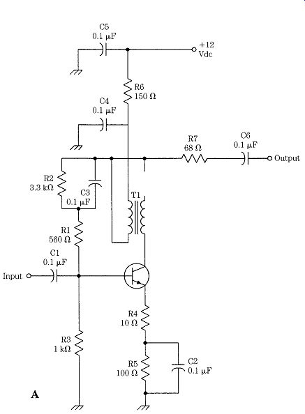
Figure 20-19 shows two popular amplifiers. They can be used for either preamplifier or postamplifier service because they each have 50-ohm input and output impedances. The circuit in Fig. 20-19A is based on the 2N5109 RF transistor and provides close to 20 dB of gain throughout the HF portion of the spectrum. A small amount of stabilizing degenerative feedback is provided by leaving part of the emitter resistance (R3) unbypassed, while properly bypassing the remaining portion of the emitter resistance. Additional feedback occurs because of the 4:1 impedance transformer in the collector circuit of the transistor. This transformer can be home brewed using an FT-44-43 or FT-50-43 toroidal ferrite core bifilar wound with 7 to 10 turns of no. 26 AWG enameled wire (or its equivalent in other countries).
20-17 SSB modulator based on LM-1496.
20-18 Product detector circuit.
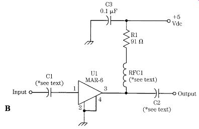
The circuit in Fig. 20-19B is based on the Mini-Circuits MAR-x series of MMIC devices. These chips provide 13- to 26-dB gain, at good noise figures, for frequencies from near-dc to 1000 MHz (or more in some models, e.g., 1500 or 2000 MHz). The MAR-1 device shown in the circuit diagram is capable of 15-dB performance to 1000 MHz.
The input and output capacitors can be disk ceramic types up to about 100 MHz, but above that frequency "chip" capacitors should be used. Values of 0.01 uF should be used in the low-HF region ( 10 MHz), 0.001 uF can be used up to 100 MHz, and 100 pF above 100 MHz. The RF choke (RFC1) should be 2.5 mH in the low-HF region, 1 mH from about 10 to 30 MHz, 100 uH from 30 to 100 MHz, and 10 uH above 100 MHz. These values are not critical and are given only as guidelines. Although it might be a bit tricky to get a 1-mH RFC to operate well at 100 MHz, there is no really hard boundary for these bands.
20-19 Post-amplifiers: (A) NPN and (B) MAR-x.
20-19 Continued.
Conclusion
Doubly balanced mixer circuits work better than most other mixer circuits in radio receivers, SSB transmitters/receivers, instrumentation, and measurement situations. They are easy to use in most cases, and, where properly designed into a circuit, they yield good results with minimum effort.
References:
Carr, J. J. (1992). NE-602 Primer, Elektor Electronics, January, pp. 20-25.
Makhinson, J. (1993). "A High Dynamic Range MF/HF Receiver Front End," QST, February, pp. 23-28.