AMAZON multi-meters discounts AMAZON oscilloscope discounts
Most modern radio transceivers (i.e., transmitter/receiver) use "relayless" switching to go back and forth between the receive and transmit states. In many cases, this switching is done with PIN diodes. Similarly, IF filters or front-end bandpass filters are selected with a front-panel switch that handles only direct current. How? Again, PIN diodes. These interesting little components allow us to do switching at RF, IF, and audio frequencies without routing the signals themselves all over the cabinet.
This section shows how these circuits work.
The P-I-N or "PIN" diode is different from the PN junction diode (see Fig. 21-1A):
it has an insulating region between the P- and N-type material (Fig. 21-1B). It is therefore a multi-region semiconductor device, despite having only two electrodes.
The I-region is not really a true semiconductor insulator but rather is a very lightly doped N-type region. It is called an intrinsic region because it has very few charge carriers to support the flow of an electrical current.
When a forward-bias potential is applied to the PIN diode, charge carriers are injected into the I-region from both N and P regions. But the lightly doped design of the intrinsic region is such that the N- and P-type charge carriers don't immediately recombine (as in PN junction diodes). There is always a delay period for recombination. Because of this delay phenomena, a small, but finite number of carriers in the I-region are always uncombined. As a result, the resistivity of the I-region is very low.
One application that results from the delay of signals passing across the intrinsic region is that the PIN diode can be used as a RF phase shifter. In some microwave antennas, phase shifting is accomplished by the use of one or more PIN diodes in series with the signal line. Although other forms of RF phase shifters (e.g., phase shifter) are usable at those frequencies, the PIN diode remains popular.
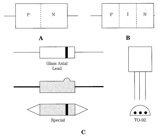
21-1 (A) PN diode, (B) PIN diode, and (C) PIN diode packages.
Figure 21-1C shows some of the package styles used for PIN diodes at small signal power levels. All but one of these shapes is familiar to most readers, although the odd-shaped flat package is probably recognized only by people with some experience in UHF (and higher) switching circuits. The NTE-553 and ECG-553 PIN diode will dissipate 200 mW and uses the standard cylindrical package style. The NTE-555 and ECG-555 device, on the other hand, uses the UHF flat package style and can dissipate 400 mW. I used these diodes for the experiments performed to write this section because they are service shop replacement lines, and both ECG and NTE are widely distributed in local parts stores. An alternative that might be harder to come by is the MPN3404, which uses the TO-92 plastic package (Fig. 21-1C).
Radio-frequency ac signals can pass through the PIN device and in fact see it under some circumstances as merely a parallel plate capacitor. We can use PIN diodes as electronic switches for RF signals and as a RF delay line or phase-shifter or as an amplitude modulator.
PIN diode switch circuits
PIN diodes can be used as switches in either series or parallel modes. Figure 21-2 shows two similar switch circuits. In the circuit of Fig. 21-2A, the diode (D1) is placed in series with the signal line. When the diode is turned on, the signal path has a low resistance; when the diode is turned off, it has a very high resistance (thus pro viding the switching action). When switch S1 is open, the diode is unbiased so the circuit is open by virtue of the very high series resistance. But when S1 is closed, the diode is forward-biased and the signal path is now a low resistance. The ratio of off/on resistances provides a measure of the isolation provided by the circuit. A pair of radio-frequency chokes (RFC1 and RFC2) are used to provide a high impedance to RF signals, while offering low dc resistance.
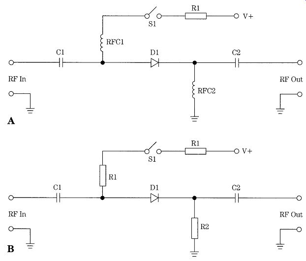
21-2 Series PIN diode switching circuits: (A) resistor loaded and (B) RF
choke loaded.
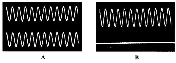
21-3 PIN diode switching action: (A) switch ON and (B) switch OFF (in both
cases upper trace is input and lower trace is output).

21-4 PIN diode switching using square-wave chopper waveform.
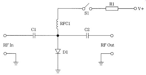
21-5 Shunt PIN diode switch.
Figure 21-2B is similar to Fig. 21-2A, except that the RF chokes are deleted and a resistor is added. Figure 21-3 shows a test that I performed on the circuit of Fig. 21-2B using a 455-kHz IF signal (the 'scope was set to show only a few cycles of the 455 kHz). The oscilloscope trace in Fig. 21-3A shows the ON position, where _12 Vdc was connected through switch S1 to the PIN diode's current-limiting resistor. This signal is 1200 mV peak-to-peak. The trace in Fig. 21-3B shows the same signal when the switch was OFF (i.e., _12 Vdc disconnected) but with the oscilloscope set to the same level. It appears to be a straight line. Increasing the sensitivity of the 'scope showed a level of 12 mV getting through. This means that this simplest circuit provides a 100:1 on/off ratio, which is 40 dB of isolation.
[Note: for this experiment, ECG-555 and NTE-555 hot-carrier PIN diodes were used].
Figure 21-4 shows the same switch when a square wave is used to drive the PIN diode control voltage line rather than _12 Vdc. This situation is analogous to a CW keying waveform. The photo represents one on/off cycle. With the resistor and capacitor values shown, a pronounced switching transient is present.
Figure 21-5 shows the circuit for a shunt PIN diode switch. In this case, the diode is placed across the signal line, rather than in series with it. When the diode is
turned off, the resistance across the signal path is high, so circuit operation is unimpeded. But when the diode is turned on (S1 closed), a near-short-circuit is placed across the line. This type of circuit is turned off when the diode is forward-biased.
This action is in contrast to the series switch, in which a forward-biased diode is used to turn the circuit on.
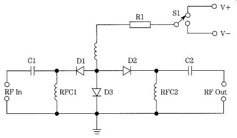
21-6 Series-shunt PIN diode switch.
A combination series-shunt circuit is shown in Fig. 21-6. In this circuit, D1 and D2 are placed in series with the signal line and D3 is in parallel with the line. D1 and D2 will turn on with a positive potential applied and D3 turns on when a negative potential is applied. When switch S1 is in the ON position, a positive potential is applied to the junction of the three diodes. As a result, D1 and D2 are forward-biased and thus take on a low resistance. At the same time, D3 is hard-reverse-biased, so it has a very high resistance. Signal is passed from input to output essentially unimpeded (most PIN diodes have a very low series resistance).
But when S1 is in the OFF position, the opposite situation obtains. In this case, the applied potential is negative, so D1/D2 are reverse-biased (and take on a high series resistance) while D3 is forward-biased (and takes on a low series resistance).
This circuit action creates a tremendous attenuation of the signal between input and output.
PIN diode applications
PIN diodes can be used as either a variable resistor or as an electronic switch for RF signals. In the latter case, the diode is basically a two-valued resistor with one value being very high and the other being very low. These characteristics open several possible applications.
When used as a switch, PIN diodes can be used to switch devices, such as attenuators, filters, and amplifiers in and out of the circuit. It has become standard practice in modern radio equipment to switch dc voltages to bias PIN diodes rather than to directly switch RF/IF signals. In some cases, the PIN diode can be used to simply short out the transmission path to bypass the device.
The PIN diode will also work as an amplitude modulator. In this application, a PIN diode is connected across a transmission line or inserted into one end of a piece of microwave waveguide. The audio modulating voltage is applied through a RF choke to the PIN diode. When a CW signal is applied to the transmission line, the varying resistance of the PIN diode causes the signal to be amplitude modulated.
A popular police radar jamming technique among another generation of "bandit techies" was to place a PIN diode in a cavity, _/4 from the rear that was resonant at the radar gun frequency and fed at its open end with a horn antenna and then modulate it with an audio sine wave equal to the doppler shift expected of either 125 or 0 MPH speeds. Don't try it, by the way, the cops have got better guns-even if they do cause an-ahem-"personal problem" when left on the seat between their legs for any length of time.
Another application is shown in Fig. 21-7. Here, a pair of PIN diodes are used as a transmit-receive (TR) switch in a radio transmitter; models from low-HF to microwave use this technique. Where you see a so-called "relayless TR switch," it is al most certain that a PIN diode network (such as Fig. 21-7) is in use. When switch S1 is open, diodes D1 and D2 are unbiased, so they present a high impedance to the signal. Diode D1 is in series with the transmitter signal so it blocks it from reaching the antenna; diode D2, on the other hand, is across the receiver input so does not attenuate the receiver input signal at all. But when switch S1 is closed, the opposite situation occurs: both D1 and D2 are now forward-biased. Diode D1 is now a low resistance in series with the transmitter output signal so the transmitter is effectively connected to the antenna. Diode D2 is also a low resistance and is across the receiver input and causes it to short out. The isolation network can be either a quarter wavelength transmission line, microstrip line designed into the printed circuit board, or a LC pi- section filter.
Transmitters up to several kilowatts have been designed using this form of switching, and almost all current VHF/UHF portable "handi-talkies" use PIN diode switching. Higher power circuits require larger diodes than were covered in this section, but they are easily available from industrial distributors.
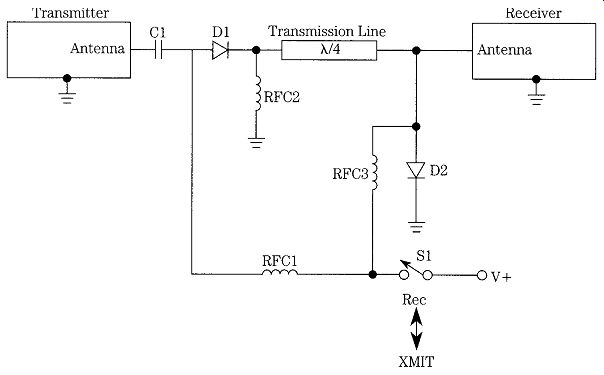
21-7 PIN diode T/R switching.
Figure 21-8 shows how multiple IF bandpass filters are selected, with only dc being routed around the cabinet between the circuitry and the front panel. A set of in put and output PIN diode switches are connected as shown and fed with a switch that selects either _12 Vdc or _12 Vdc alternately. When the switch is in the position shown, the _12 V is to the filter 1 switches, so filter 1 is activated. When the switch is in the opposite position, the alternate filter is turned on. This same arrangement can be used in the front end of the receiver, or the local oscillator, to select LC components for different bands.
Another filter selection method is shown in Fig. 21-9. This circuit is a partial representation of the front-end circuitry for the Heathkit SW-7800 general-coverage shortwave receiver. The entire circuit differs from this variant in that a total of six filter sections are used rather than just two (Fig. 21-9). In each bandpass filter (BPF1 and BPF2), a network of inductor and capacitor elements are used to set the center and both edge frequencies of the band to be covered.
The circuit of Fig. 21-9 uses a switch (S1) to apply or remove the _12-Vdc bias potential on the diodes, but in the actual receiver, this potential is digitally con trolled. The digital logic elements sense which of 30 bands are being used and selects the input RF filter accordingly.
Another application for PIN diodes is as a voltage-variable attenuator in RF circuits. Because of its variable resistance characteristic, the PIN diode can be used in a variety of attenuator circuits. One of the simplest is the shunt attenuator of Fig. 21-10. The front end of this circuit is a bank of selectable bandpass filters per 21-8 PIN diode bandpass filter switching.
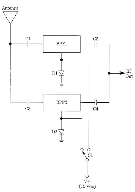
21-9 RF input receiver bandpass filter switching.
Fig. 21-9, so we will not dwell on that topic now. But at the output of the filter bank is a shunted from the signal line to ground a series combination of a capacitor (C1) and a PIN diode (D1).
The PIN diode acts like an electronically variable resistor. The resistance across the diode's terminals is a function of the applied bias voltage. This voltage, hence the degree of attenuation of the RF signal, is proportional to the setting of potentiometer, R1. The series resistor (R2) is used to limit the current when the diode is forward-biased. This step is necessary because the diode becomes a very low resistance when a certain rather low potential is exceeded. This circuit is used as a RF gain control on some modern receivers. Another PIN diode attenuator circuit (the "bridge-tee" attenuator) is shown in Fig. 21-10. It is capable of providing a 10-dB attenuation range over a very wide bandwidth.
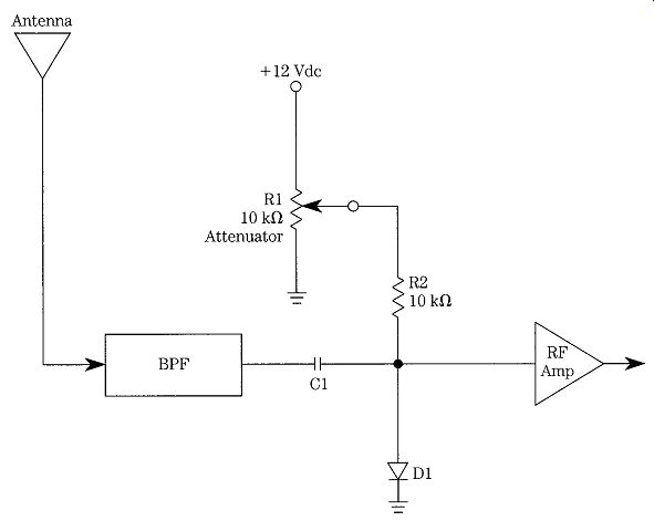
21-10 PIN diode RF attenuator.
Conclusion
PIN diodes are little known but are nonetheless very useful. If you build any RF projects that could involve traditional switching then you will probably find that the PIN diode makes a dandy substitute, which avoids the problems associated with routing signal around switching circuits. Try it; you'll like it.