AMAZON multi-meters discounts AMAZON oscilloscope discounts
Very few people needed to know anything about microwaves and microwave devices- until now. For many decades, all service technicians and others only needed to know about devices that worked up to the highest UHF TV channel, which was just short of the microwave region. Even then, many local servicers would consider the entire UHF TV tuner as a black box component and replace it as a unit when it went bad.
But today, with satellite TVRO units increasingly popular, two-way communications heading into the low-microwave region, and a host of other applications on those frequencies, it becomes necessary for the service technician to learn the ins and outs of the solid-state devices used on microwave frequencies. This section takes a close look at solid-state microwave devices.
Diode devices
Diode. “Di” means "two", and -ode is derived from "electrode." Thus, the word "diode" refers to a two-electrode device. Although in conventional low-frequency solid-state terminology, the word diode indicates only PN junction diodes; in the microwave world, we see both PN diodes and others as well. Some diodes, for example, are multi-region devices, and still others have but a single semiconductor region. The latter depend on bulk-effect phenomena to operate. This section examines some of the various microwave devices that are available on the market.
World War II created a huge leap in microwave capabilities because of the needs of the radar community. Even though solid-state electronics was in its infancy, developers were able to produce crude microwave diodes for use primarily as mixers in superheterodyne radar receivers. Theoretical work done in the late 1930s, 1940s, and early 1950s predicted microwave diodes that would be capable of not only nonlinear mixing in superheterodyne receivers, but also of amplification and oscillation as well. These predictions were carried forward by various researchers. By 1970, a variety of commercial devices were on the market.
22-1 PN junction diode.
Early microwave diodes
The development of solid-state microwave devices suffered the same sort of problems as microwave vacuum tube development. Just as electron transit time limits the operating frequency of vacuum tubes, a similar phenomena affects semiconductor devices. The transit time across a region of semiconductor material is determined not only by the thickness of the region, but also by the electron saturation velocity, about 107 cm/s, which is the maximum velocity attainable in a given material. In addition, minority carriers are in a "storage" state that prevents them from being easily moved, causing a delay that limits the switching time of the device.
Also, like the vacuum tube, interelectrode capacitance limits the operating frequency of solid-state devices. Although turned to an advantage in variable capacitance diodes, capacitance between the N and P regions of a PN junction diode seriously limits operating frequency and/or switching time.
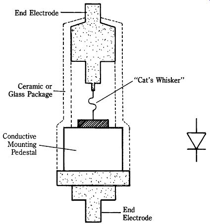
During World War II, microwave diode (such as the 1N21 and 1N23) devices were developed. The capacitance problem was partially overcome by using the point contact method of construction (shown in Fig. 22-1). The point contact diode uses a "cat's whisker" electrode to effect a connection between the conductive electrode and the semiconductor material.
Point contact construction is a throwback to the very earliest days of radio when a commonly used detector in radio receivers was the naturally occurring galena crystal (a lead compound). Those early "crystal set" radios used a cat's whisker electrode to probe the crystal surface for the spot where rectification of radio signals could occur.
The point contact diode of World War II was used mainly as a mixer element to produce an intermediate frequency (IF) signal that was the difference between a radar signal and a local oscillator (LO) signal. Those early superheterodyne radar receivers did not use RF amplifier stages ahead of the mixer, as was common in lower frequency receivers. Although operating frequencies to 200 GHz have been achieved in point contact diodes, the devices are fragile and are limited to very low power levels.
Schottky barrier diodes The Schottky diode (also called the hot carrier diode) is similar in mechanical structure to the point contact diode, but is more rugged and is capable of dissipating more power. The basic structure of the Schottky diode is shown in Fig. 22-2A, and the equivalent circuit is shown in Fig. 22-2B. This form of microwave diode was predicted in 1938 by William Schottky during research into majority carrier rectification phenomena.
A "Schottky barrier" is a quantum mechanical potential barrier set up by virtue of a metal to semiconductor interface. The barrier is increased by increasing reverse bias potential and reduced (or nearly eliminated) by forward-bias potentials. Under reverse-bias conditions, the electrons in the semiconductor material lack sufficient energy to breach the barrier, so no current flow occurs. Under forward-bias conditions, however, the barrier is lowered sufficiently for electrons to breach it and flow from the semiconductor region into the metallic region.
The key to junction diode microwave performance is its switching time, or switching speed as it is sometimes called. In general, the faster the switching speed (i.e., shorter the switching time), the higher the operating frequency. In ordinary PN junction diodes, switching time is dominated by the minority carriers resident in the semiconductor materials. The minority carriers are ordinarily in a rest or "storage" state so are neither easily nor quickly swept along by changes in the electric field potential. But majority carriers are more mobile, so respond rapidly to potential changes. Thus, Schottky diodes, by depending on majority carriers for switching operation, operate with very rapid speeds-well into the microwave region for many models.
Operating speed is also a function of the distributed circuit RLC parameters (see Fig. 22-2B). In Schottky diodes that operate into the microwave region, series resistance is about 3 to 10 ohm, capacitance is around 1 pF and series lead inductance tends to be 1 nH or less.
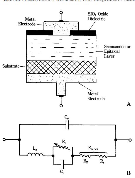
22-2 (A) Schottky barrier diode and (B) equivalent circuit.
The Schottky diode is basically a rectifying element, so it finds a lot of use in mixer and detector circuits. The double balanced mixer (DBM) circuit, which is used for a variety of applications from heterodyning to the generation of double sideband suppressed-carrier signals to phase sensitive detectors, is usually made from matched sets of Schottky diodes. Many DBM components work into the low end of the microwave spectrum.
Tunnel diodes
The tunnel diode was predicted by L. Esaki of Japan in 1958 and is often referred to as the "Esaki diode." The tunnel diode is a special case of a PN junction diode in which carrier doping of the semiconductor material is on the order of 1019 or 1020 atoms per cubic centimeter, or about 10 to 1000 times higher than the doping used in ordinary PN diodes. The potential barrier formed by the depletion zone is very thin; on the order of 3 to 100 angstroms, or about 10^-6 cm. The tunnel diode operates on the quantum mechanical principle of tunneling (hence its names), which is a majority carrier event. Ordinarily, electrons in a PN junction device lack the energy required to climb over the potential barrier created by the depletion zone under reverse-bias conditions. The electrons are thus said to be trapped in a "potential well." The current, therefore, is theoretically zero in that case. But if the carriers are numerous enough, and the barrier zone is thin enough, then tunneling will occur.
That is, electrons will disappear on one side of the barrier (i.e., inside the potential well) and then reappear on the other side of the barrier to form an electrical current.
In other words, they appear to have tunneled under or through the potential barrier in a manner that is said to be analogous to a prisoner tunneling through the wall of the jailhouse.
Do not waste a lot of energy attempting to explain tunneling phenomena, for indeed even theoretical physicists do not understand the phenomena very well.
The tunneling explanation is only a metaphor for a quantum event that has no corresponding action in the non-atomic world. The electron does not actually go under, over, or around the potential barrier but rather it disappears here and then reappears elsewhere. Although the reasonable person is not comfortable with such seeming magic, until more is known about the quantum world, we must be content with accepting tunneling as merely a construct that works for practical purposes. All that we can state for sure about tunneling is that if the right conditions are satisfied then there is a certain probability per unit of time that tunneling will occur.
There are three basic conditions that must be met to ensure a high probability of tunneling occurring:
1. Heavy doping of the semiconductor material to ensure large numbers of majority carriers;
2. Very thin depletion zone (3 to 100 A); and
3. For each tunneling carrier, there must be a filled energy state from which it can be drawn on the source side of the barrier, and an available empty state of the same energy level to which it can go on the other side of the barrier.
Figure 22-3 shows an I-vs-V curve for a tunnel diode. Notice the unusual shape of this curve. Normally, in familiar materials that obey Ohm's law, the current (I ) will increase with increasing potential (V) and decrease with decreasing potential. Such behavior is said to represent positive resistance (_R) and is the behavior normally found in common conductors. But in the tunnel diode, there is a negative resistance zone (NRZ in Fig. 22-3) in which increasing potential forces a decreasing current.
Points A, B, and C in Fig. 22-3 show us that tunnel diodes can be used in mono stable (A and C), bistable (flip-flop from A-to-C or C-to-A), or astable (oscillate about B) modes of operation, depending on applied potential. These modes give us some insight into typical applications for the tunnel diode: switching, oscillation, and amplification. A tunnel diode has a negative resistance (_R) property, which indicates the ability to oscillate in relaxation oscillator circuits. Unfortunately, the power output levels of the tunnel diode are restricted to only a few milliwatts because the applied dc potentials must be less than the bandgap potential for the specific diode.
Figure 22-4A shows the usual circuit symbol for the tunnel diode, and Fig. 22-4B shows a simplified, but adequate, equivalent circuit. The tunnel diode can be modeled as a negative resistance element shunted by the junction capacitance of the diode. The series resistance is the sum of contact resistance, lead resistance, and bulk material resistances in the semiconductor material, and the series inductance is primarily lead inductance.
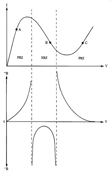
22-3 Tunnel diode characteristic curves
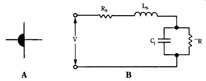
22-4 (A) Tunnel diode symbol and (B) equivalent circuit.
The tunnel diode will oscillate if the total reactance is zero (XL _Xc _0), and if the negative resistance balances out the series resistance. We can calculate two distinct frequencies with regard to normal tunnel diodes: resistive frequency (Fr) and the self resonant frequency (Fs). These frequencies are given by the following equations.
Resistive frequency:
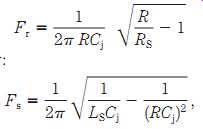
(22-1)
Self-resonant frequency:

(22-2)
where
Fr = the resistive frequency in hertz (Hz)
Fs =the self-resonant frequency in hertz (Hz)
R =the absolute value of the negative resistance in ohms
RS = the series resistance in ohms
Cj = the junction capacitance in farads
LS = the series inductance in henrys.
The negative resistance phenomena, also called negative differential resistance (NDR), is a seemingly strange phenomena in which materials behave electrically contrary to Ohm's law. In ohmic materials (i.e., those that obey Ohm's law), we normally expect current to increase as electric potential increases. In these "positive resistance" materials, I = V/R. In negative resistance (NDR) devices, however, there might be certain ranges of applied potential in which current decreases with increasing potential.
In addition to the I-vs-V characteristic, certain other properties of negative resistance materials distinguish them from ohmic materials. First, in ohmic materials, we normally expect to find the voltage and current in phase with each other unless an inductive or capacitive reactance is also present. Negative resistance, however, causes current and voltage to be 180_ out of phase with each other. This relationship is a key to recognizing negative resistance situations. Another significant difference is that a positive resistance dissipates power and negative resistance generates power (i.e., converts power from a dc source to another form). In other words, a _R device absorbs power from external sources and a _R device supplies power (converted from dc) to the external circuit.
Two forms of oscillatory circuit are possible with NDR devices: resonant and un resonant. In the resonant type, depicted in Fig. 22-5, current pulses from the NDR device shock excite a high-Q LC tank circuit or resonant cavity into self-excitation.
The oscillations are sustained by repetitive re-excitation. Un-resonant oscillator circuits use no tuning. They depend on the device dimensions and the average charge carrier velocity through the bulk material to determine operating frequency. Tunnel diodes generally work in the resonant mode. Some NDR devices, such as the Gunn, will operate in either resonant or un-resonant oscillatory modes.
Introduction to negative resistance (-R) devices
Earlier, you were introduced to the concept of negative resistance (-R) and its inverse, negative conductance (_G _ 1/_R). To review the facts, the negative resistance phenomena, also called negative differential resistance (NDR), is a seemingly strange phenomena in which materials behave electrically contrary to Ohm's law. In ohmic materials (i.e., those that obey Ohm's law), we normally expect current to increase as electric potential increases. In these "positive resistance" materials, I _ V/R. In negative resistance (NDR) devices, however, there might be certain ranges of applied potential in which current decreases with increasing potential.
In addition to the strange I-vs-V characteristic, certain other properties of negative resistance materials distinguish them from ohmic materials. First, in ohmic materials, we normally expect to find the voltage and current in-phase with each other, unless an inductive or capacitive reactance is also present. Negative resistance, how ever, causes current and voltage to be 180 degr. out of phase with each other. This relationship is a key to recognizing negative-resistance situations.
22-5 Negative resistance oscillator circuit.
In the resonant type of negative resistance circuit, depicted in Fig. 22-5, current pulses from the NDR device shock excite a high-Q LC tank circuit or resonant cavity into self-excitation. The oscillations are sustained by repetitive re-excitation. Un-resonant oscillator circuits use no tuning. They depend on the device dimensions and the average charge carrier velocity through the bulk material to determine operating frequency. Some NDR devices, such as the Gunn diode (later in this section), will operate in either resonant or un-resonant oscillatory modes.
Transferred electron devices (e.g., Gunn diodes) Gunn diodes are named after John B. Gunn of IBM, who, in 1963, discovered a phenomenon since then called the Gunn Effect. Experimenting with compound semiconductors such as gallium arsenide (GaAs), Gunn noted that the current pulse became unstable when the bias voltage increased above a certain crucial threshold potential. Gunn suspected that a negative resistance effect was responsible for the unusual diode behavior. Gunn diodes are representative of a class of materials called transferred electron devices (TED).
Ordinary two-terminal small-signal PN diodes are made from elemental semi conductor materials, such as silicon (Si) and germanium (Ge). In the pure form be fore charge carrier doping is added, these materials contain no other elements. TED devices, on the other hand, are made from compound semiconductors; that is, materials that are chemical compounds of at least two chemical elements. Examples are gallium arsenide (GaAs), indium phosphide (InP), and cadmium telluride (CdTe). Of these, GaAs is the most commonly used.
N-type GaAs used in TED devices is doped to a level of 1014 to 1017 carriers per centimeter at room temperature (373_K). A typical sample used in TED/Gunn de vices will be about 150-ohm 150-ohm M in cross- sectional area and 30 _M long.
Two-valley TED model
The operation of TED devices depends on a semiconductor phenomenon found in compound semiconductors called the two-valley model (for InP material, there is also a three-valley model). The two-valley model is also called the Ridley/ Watkins/ Hilsum theory. Figure 22-6 shows how this model works in TEDs. In ordinary elemental semiconductors, the energy diagram shows three possible bands: valence band, forbidden band, and conduction band. The forbidden band contains no allow able energy states so it contains no charge carriers. The difference in potential be tween valence and conduction bands defines the forbidden band, and this potential is called the bandgap voltage.
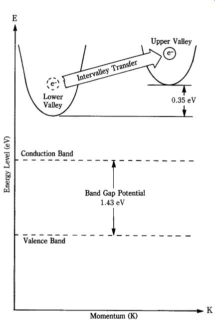
22-6 Transferred electron diode operation.
In the two-valley model, however, there are two regions in the conduction band in which charge carriers (e.g., electrons) can exist. These regions are called valleys and are designated the upper valley and the lower valley. According to the RWH theory, electrons in the lower valley have low effective mass (0.068) and consequently a high mobility (8000 cm^2/V-s). In the upper valley, which is separated from the lower valley by a potential of 0.036 electron volts (eV), electrons have a much higher effective mass (1.2) and lower mobility (180 cm^2/V-s) than in the lower valley.
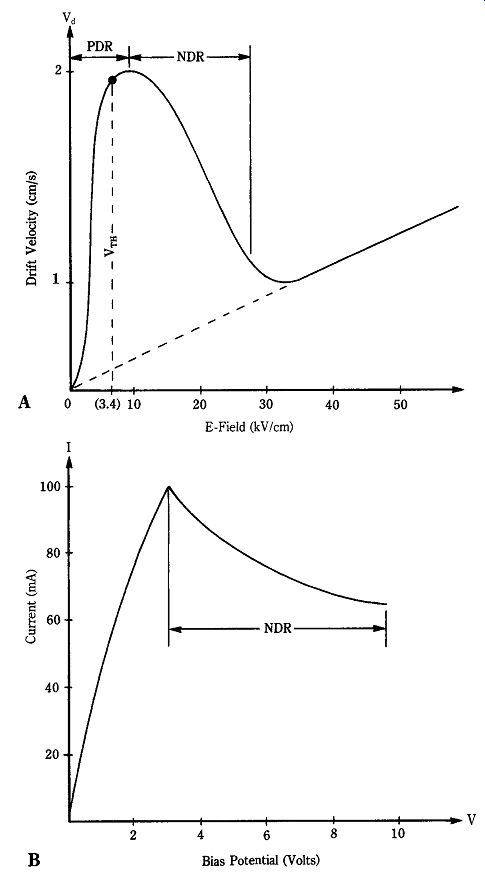
At low electric field intensities (0 to 3.4 kV/cm), electrons remain in the lower valley and the material behaves ohmically. At these potentials, the material exhibits positive differential resistance (PDR). At a certain critical threshold potential (Vth), electrons are swept from the lower valley to the upper valley (hence the name transferred electron devices). For GaAs the electric field must be about 3.4 kV/cm, so Vth is the potential that produces this strength of field. Because Vth is the product of the electric field potential and device length, a 10-_M sample of GaAs will have a thresh old potential of about 3.4 V. Most GaAs TED devices operate at maximum dc potentials in the 7- to 10-V range.
The average velocity of carriers in a two-valley semiconductor (such as GaAs) is a function of charge mobility in each valley and the relative numbers of electrons in each valley. If all electrons are in the lower valley then the material is in the highest average velocity state. Conversely, if all electrons were in the upper valley, then the average velocity is in its lowest state. Figure 22-7A shows drift velocity as a function of electric field, or dc bias.
22-7 (A) Drift velocity vs electric field, (B) I-vs-I_bias, and (C) diode
current vs time.
22-7 Continued.
In the PDR region, the GaAs material is ohmic, and the drift velocity increases linearly with increasing potential. It would continue to increase until the saturation velocity is reached (about 107 cm/s). As the voltage increases above threshold potential, which creates fields greater than 3.4 kV/cm, more and more electrons are transferred to the upper valley so that the average drift velocity drops. This phenomena gives rise to the negative resistance (NDR) effect. Figure 22-7B shows the NDR effect in the I-vs-V characteristic.
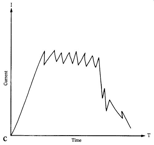
Figure 22-7C shows the I-vs-T characteristic of the Gunn diode operating in the NDR region. Ordinarily, you would expect a smooth current pulse to propagate through the material. But notice the oscillations (i.e., Gunn's instabilities) superimposed on the pulse. This oscillating current makes the Gunn diode useful as a microwave generator.
For the two-valley model to work, several criteria must be satisfied. First, the energy difference between lower and upper valleys must be greater than the thermal energy (KT) of the material; KT is about 0.026 eV, so GaAs with 0.036 eV differential energy satisfies the requirement. Second, in order to prevent hole-electron pair formation the differential energy between valleys must be less than the forbidden band energy (i.e., the bandgap potential). Third, electrons in the lower valley must have high mobility, low density of state, and low effective mass. Finally, electrons in the upper valley must be just the opposite: low mobility, high effective mass, and a high density of state. It is sometimes claimed that ordinary devices use so-called "warm" electrons (i.e., 0.026 eV) and TED devices use "hot" electrons greater than 0.026 eV.
22-8 (A) Gunn diode and (B) equivalent circuit.
Gunn diodes
The Gunn diode is a transferred electron device that is capable of oscillating in several modes. In the un-resonant transit-time (TT) mode, frequencies between 1 and 18 GHz are achieved, with output powers up to 2 W (most are on the order of a few hundred milliwatts). In the resonant limited space-charge (LSA) mode, operating frequencies to 100 GHz and pulsed power levels to several hundred watts (1% duty cycle) have been achieved.
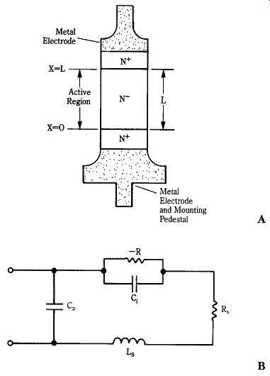
Figure 22-8A shows a diagram for a Gunn diode, and an equivalent circuit is shown in Fig. 22-8B. The active region of the diode is usually 6 to 18 _m long. The N_ end regions are ohmic materials of very low resistivity (0.001 _-cm), and are 1 to 2 _m thick. The function of the N_ regions is to form a transition zone between the metallic end electrodes and the active region. In addition to improving the contact, the N_ regions prevent migration of metallic ions from the electrode into the active region.
22-9 Domain formation and propagation.
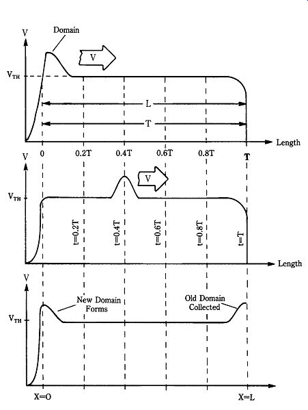
Domain growth
The mechanism underlying the oscillations of a Gunn diode is the growth of Ridley domains in the active region of the device. An electron domain is created by a bunching effect (Fig. 22-9) that moves from the cathode end to the anode end of the active region. When an old domain is collected at the anode, a new domain forms at the cathode and begins propagating. The propagation velocity is close to the saturation velocity (10^7 cm/s). The time required for a domain to travel the length (L) of the material is called the transit time (Tt), which is:

(22-3)
.......where.....
Tt _ the transit time in seconds (s)
L _ the length in centimeters (cm)
Vs _ the saturation velocity (10^7 cm/s)
22-10 Domain formation in semiconductor material.
Figure 22-10 graphically depicts domain formation. You might recognize that the "domain" shown here is actually a dipole, or double domain. The area ahead of the domain forms a minor depletion zone, and in the area of the domain, there is a bunching of electrons. Thus, there is a difference in conductivity between the two regions, and this conductivity is different still from the conductivity of the rest of the active region. There is also a difference between the electric fields in the two domain poles and also in the rest of the material. The two fields equilibrate outside of the domain. The current density is proportional to the velocity of the domain, so a current pulse forms.
Gunn operating modes Transferred electron devices (i.e., Gunn diodes) operate in several modes and sub-modes. These modes depend in part on device characteristics and in part on external circuitry. For the Gunn diode, the operating modes are stable amplification (SA) mode, transit time (TT) mode, limited space-charge (LSA) mode, and bias circuit oscillation (BCO) mode.
Stable amplification (SA) modes In this mode, the Gunn diode will behave as an amplifier. The requirement for SA-mode operation is that the product of doping concentration (No) and effective length of the active region (L) must be less than 10^12/cm^2. Amplification is limited to frequencies in the vicinity of v/L, where v is the domain velocity and L is the effective length.
Transit time (Gunn) mode The transit time (TT), or Gunn, mode is un-resonant and depends on device length and applied dc bias voltage. The dc potential must be greater than the critical threshold potential (Vth). Because of the Gunn effect, current oscillations in the microwave region are superimposed on the current pulse. Operation in this mode requires that the No L product be 10^12/cm^2 to 10^14/cm^2. Operating frequency Fo is determined by device length, or rather the transit time of the pulse through the length of the material. Because domain velocity is nearly constant, and is often close to the electron saturation velocity (Vs= 10^7 cm/s), length and transit time are proportional to each other. The operating frequency is inversely proportional to both the length of the device and the transit time.
The length of the active region in the Gunn diode determines operating frequency.
The frequency varies from about 6 GHz for an 18-_m sample (counting 1.5 _m for each N_ electrode region) to 18 GHz for a 6-_m sample. The operating frequency in the TT mode is approximately:

(22-4)
......
where......
Fo _ the operating frequency in hertz (Hz) Vdom _ the domain velocity in centimeters per second (cm/s) Leff _ the effective length in centimeters (cm)
Operation in the TT mode provides efficiencies of 10% or less, with 4 to 6% being most common. Output powers are usually less than 1000 mW, although 2000 mW has been achieved.
22-11 (A) Oscillator circuit for negative resistance mode, (B) characteristic
waveforms of circuit, and (C) output voltage.
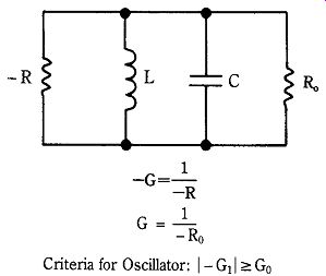
Limited space charge (LSA) mode The LSA mode depends on shock ex citing a high-Q resonant tank circuit or tuned cavity with current pulses from the Gunn diode. The LSA mode and its sub-modes are also called accumulation mode, delayed domain mode, and quenched domain mode. These various names reflect variations on the LSA theme. For the LSA mode, the No L product must be 10^12/cm^2 or higher and the No/F quotient must be between 2 _ 10^5 and 2 _ 10^4 s/cm^3.
Figure 22-11A shows a simplified circuit for a LSA-mode Gunn oscillator, and Fig. 22-11B shows the waveforms. The circuit consists of the Gunn diode shunted by either a LC tank circuit (as shown) or a tuned cavity that behaves like a tank circuit. The criterion for resonant oscillation in a negative resistance circuit is simple: the negative conductance (_G _ 1/_R) must be greater than or equal to the conductance represented by circuit losses:

(22-5)
22-12 LSA output pulses.
At turn-on, transit time current pulses (Fig. 22-12) hit the resonant circuit and shock excite it into oscillations at the resonant frequency. These oscillations set up a sine-wave voltage across the diode (Fig. 22-12) that adds to the bias potential. The total voltage across the diode is the algebraic sum of the dc bias voltage and the RF sine-wave voltage. The dc bias is set so that the negative swing of the sine wave forces the total voltage below the critical threshold potential, Vth. Under this condition, the domain does not have time to build up and the space charge dissipates. The domain quenches during the period when the algebraic sum of the dc bias and the sine-wave voltage is below Vth. The LSA oscillation period (T _ 1/F) is set by the external tank circuit and the diode adapts to it. The period of oscillation is found from:
(22-6) ...
.... where ...
T _ the period in seconds (s) L _ the inductance in henrys (H) C _ the capacitance in farads (F) R _ the low-field resistance in ohms (_) Vth _ the threshold potential Vb _ the bias voltage.
The LSA mode is considerably more efficient than the transit-time mode. The LSA mode is capable of 20% efficiency so that you can produce at least twice as much RF output power from a given level of dc power drawn from the power supply as transit time operation. At duty factors of 0.01, the LSA mode is capable of delivering hundreds of watts of pulsed output power. The output power of any oscillator or amplifier is the product of three factors: dc input voltage (V), dc input current (I), and the conversion efficiency (n, a decimal fraction between 0 and 1):

(22-7)
where Po _ the output power n _ the conversion efficiency factor (0-1) V _ the applied dc voltage I _ the applied dc current For the Gunn diode case, a slightly modified version of this expression is used:

(22-8)
... where ...
n _ the conversion efficiency factor (0-1) v _ the average drift velocity Vth _ the threshold potential (kV/cm) M _ the multiple Vdc/Vth L _ the length in centimeters no _ the donor concentration e _ the electric charge (1.6 _ 10_19 coulomb) A _ the area of the device in cm2 Bias circuit oscillation (BCO) Gunn mode This mode is quasi-parasitic in nature and occurs only during one of the normal Gunn oscillating modes (TT or LSA).
If product F1 is very, very small then BCO oscillations can occur at frequencies from 0.01 to 100 MHz.
Gunn diode applications
Gunn diodes are often used to generate microwave RF power in diverse applications ranging from receiver local oscillators, to police speed radars, to microwave communications links. Figure 22-13 shows two possible methods for connecting a Gunn diode in a resonant cavity. Figure 22-13A shows a cavity that uses a loop coupled output circuit. The output impedance of this circuit is a function of loop size and position, with the latter factor dominating. The loop positioning is a trade-off be tween maximum output power and oscillator frequency stability.
Figure 22-13B shows a Gunn diode mounted in a section of flanged waveguide.
RF signal passes through an iris to be propagated through the waveguide to the load.
In both Figs. 22-13A and 22-13B, the exact resonant frequency of the cavity is set by a tuning screw inserted into the cavity space.
22-13 (A) Gunn diode operated in a cavity and (B) Gunn diode in a cavity
antenna.
IMPATT diodes
The avalanche phenomenon is well-known in PN junction diodes. If a reverse bias potential exceeds a certain critical threshold, then the diode breaks down and the reverse current increases abruptly from low "leakage" values to a very high value. The principal cause of this phenomena is secondary electron emission (i.e., charge carriers become so energetic as to be able to knock additional valence electrons out of the crystal lattice to form excess hole-electron pairs). The common zener diode works on this principle.
The onset of an avalanche current in a PN junction is not instantaneous, but rather, there is a short phase-delay period between the application of a sufficient breakdown potential and the creation of the avalanche current. In 1959, W. T. Read of Bell Telephone Laboratories postulated that this phase delay could create a negative resistance. It took until 1965 for others (Lee and Johnson) at Bell Labs to create the first of these "Read diodes." Johnson generated about 80 mW at 12 GHz in a silicon PN junction diode. Today, the class of diodes of which the Read device is a member are referred to collectively as Impact Avalanche Transit Time (IMPATT) diodes.
The name IMPATT reflects the two different mechanisms at work: Avalanche (impact ionization) and Transit time (drift).
22-14 IMPATT diode characteristic waveforms.
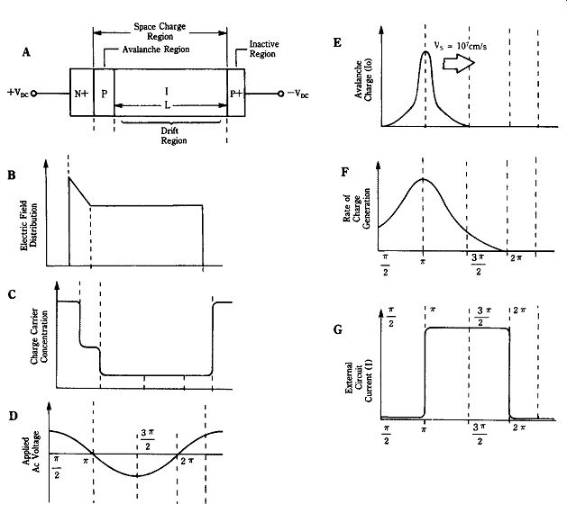
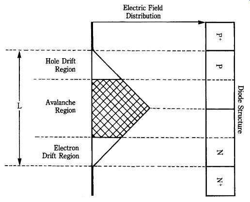
Figure 22-14 shows a typical IMPATT device based on a N_-P-I-P_ structure.
Other structures are also known, but the NPIP of Fig. 22-14A is representative. The "_" indicates a higher than normal doping concentration, as indicated by the profile in Fig. 22-14C. The doping profile ensures an electric field distribution (Fig. 22-14B) that is higher in the P region in order to confine avalanching to a small zone. The I region is an intrinsic semiconductor that is lightly doped to have a low charge carrier density. Thus, the I region is a near insulator, except when charge carriers are injected into it from other regions.
The IMPATT diode is typically connected in a high-Q resonant circuit (LC tank or cavity). Because avalanching is a very noisy process, noise at turn-on "rings" the tuned circuit and creates a sine-wave oscillation at its natural resonant frequency (Fig. 22-14D). The total voltage across the NPIP structure is the algebraic sum of the dc bias and tuned-circuit sine wave.
The avalanche current (Io) is injected into the I region and begins propagating over its length. Notice in Fig. 22-14E that the injected current builds up exponentially until the sine wave crosses zero then drops exponentially until the sine wave reaches the negative peak. This current pulse is thus delayed 90 degr. with respect to the applied voltage.
Compare now the external circuit current pulse in Fig. 22-14G with the tuned circuit sine wave (Fig. 22-14D). Notice that transit time in the device has added additional phase delay, so the current is 180 degr. out of phase with the applied voltage.
This phase delay is the cause of the negative resistance characteristic. Oscillation is sustained in the external resonant circuit by successive current pulses re-ringing it.
The resonant frequency of the external resonant circuit should be:

(22-9)
....where....
F = the frequency in hertz (Hz)
Vd = the drift velocity in centimeters per second (cm/s)
L = the length of the active region in centimeters (cm)
IMPATT diodes typically operate in the 3- to 6-GHz region, although 100-GHz operation has been achieved. These devices typically operate at potentials in the 75 to 150-Vdc range. Because an avalanche process is used, the RF output signal of the IMPATT diode is very noisy. Efficiencies of single drift-region devices (such as Fig. 22-14A) are about 6 to 15%. By using double-drift construction (Fig. 22-15), efficiencies can be improved to the 20 to 30% range. The double-drift device uses electron conduction in one region and hole conduction in the other. This operation is possible because the two forms of charge carrier drift approximately in phase with each other.
22-15 PPNN double-drift IMPATT diode.
22-16 TRAPATT diode.
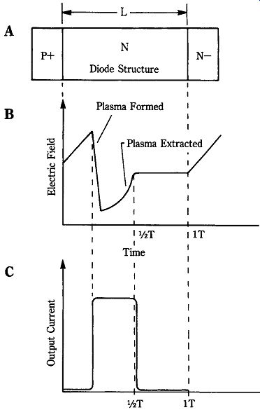
TRAPATT diodes
Gunn and IMPATT diodes operate at frequencies of 3 GHz or above. Operation at lower frequencies (e.g., 500 MHz to 3 GHz) was left to transistor, which also limited available RF output power to a great extent. Gunn and IMPATT devices cannot operate at lower frequencies because it was difficult to increase transit time in those devices. You might assume that it is only necessary to lengthen the active region of the device to increase transit time. But certain problems arose in long structures, domains were found to collapse, and sufficient fields were hard to maintain.
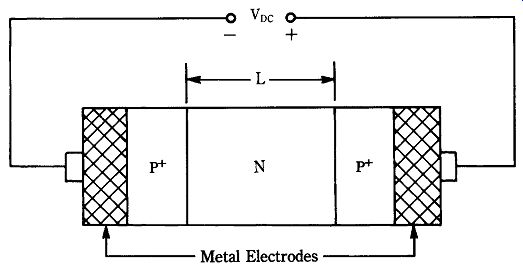
A solution to the transit time problem is found in a modified IMPATT structure that uses P_-N-N_ regions (Fig. 22-16). The P_ region is typically 3 to 8 _M, and the N-region is typically 3 to 13 _m. The diameter of the device might be 50 to 750-ohm m, depending on the power level required. The first of these diodes was produced by RCA in 1967. It produced more than 400 W at 1000 MHz, at an efficiency of 25%. Since then, frequencies as low as 500 MHz, and powers to 600 W, have been achieved. Today, efficiencies in the 60 to 75% range are common. One device was able to provide continuous tuning over a range of 500 to 1500 MHz.
The name of the P_-N-N- device reflects its operating principle: trapped plasma avalanche triggered transit (TRAPATT)-the method by which transit time is increased by formation of a plasma in the active region. A plasma is a region of a large number of disassociated holes and electrons that do not easily recombine. If the electric field is low, then the plasma is trapped. That is, the charge carriers are swept out of the N region slowly (see Fig. 22-16B).
The output is a harmonic-rich, sharp rise-time current pulse (Fig. 22-16C). To become self-oscillatory, this pulse must be applied to a low-pass filter at the input of the transmission line or waveguide that is connected to the TRAPATT. Harmonics are not passed by the filter, so they are reflected back to the TRAPATT diode to trigger the next current pulse.
BARITT diodes
The BARITT diode (Fig. 22-17) consists of three regions of semiconductor material forming a pair of abrupt PN junctions, one each P_-N and N-P_. The name of this device comes from a description of its operation: barrier injection transit time.
The BARITT structure is designed so that the electric field applied across the end electrodes causes a condition at or near punch-through. That is, the depletion zone is formed throughout the entire N region of the device. Current is formed by sweeping holes into the N region of the device. Under ordinary circumstances, the P_-N junction is forward-biased and the N-P_ is reverse-biased. The depleted N region forms a potential barrier into which holes are injected into the N region from the forward-biased junction. These charge carriers then drift across the N region at the saturation velocity of 107 cm/sec, forming a current pulse. There are three conditions for proper BARITT operation.
22-17 BARITT diode.
The electrical field across the device must be great enough to force charge carriers in motion to drift at the saturation velocity (107 cm/s); The electrical field must be great enough to create the punch-through condition, and the electrical field must not be great enough to cause avalanching to occur.
The normal circuit configuration for BARITT devices is in a resonant LC tank or cavity. At turn-on, noise pulses will initially shock-excite the resonant circuit into self-oscillation, and successive current pulses supply the energy to continue the oscillations. Figure 22-18 shows the relationship between the oscillatory sine-wave voltage, the internal current, and the external current. As in the other diodes, the output energy comes from tapping the energy in the resonant circuit.
22-18 Characteristic waveforms.
UHF and microwave RF transistors
Transistors were developed right after World War II and by 1955 were being used in consumer products. Those early devices were limited to audio and low-RF frequencies, however. As a result, only solid-state audio products and AM-band radios were widely available in the 1950s. Development continued, however, and by 1963, solid-state FM broadcast and VHF communications receivers were on the market. Microwave applications, however, remained elusive.
Early transistors were severely frequency-limited by a number of factors, including electron saturation velocity, base structure thickness (which affects transit time), base resistance, and device capacitances. In the latter category are junction capacitances and stray capacitances resulting from packaging. When combined with stray circuit inductances and circuit resistances, the device capacitance significantly rolled-off upper operating frequencies.
The solution to the operating frequency limitation was in developing new semi conductor materials (e.g., gallium arsenide, different device internal geometries, and new device construction and packaging methods). Today, transistor devices operate well into the microwave region, and 40-GHz devices are commercially obtainable; 90-GHz devices have been demonstrated in Japanese laboratories. Transistors have replaced other microwave amplifiers in many applications-especially in low-noise receiver amplifiers.
Table 22-1. Mobility (cm^2/V-s)
Semiconductor overview
Semiconductors fall into a gray area between good conductors and poor conductors (i.e., insulators). The conductivity of these materials can be varied by "doping" with impurities, changes in temperature and by light (as in the case of phototransistors). Prior to the development of microwave transistors, most devices were made of Group IV-A materials, such as silicon (Si) and germanium (Ge). The term Group IV-A refers to the group occupied by these materials on the Periodic Table of chemical elements. Some modern microwave transistors are made of Group III-A semiconductors, such as gallium and indium (see Table 22-1).
Figure 22-19 shows an energy level diagram for semiconductor materials. Two permissible bands represent states that are allowed to exist: the conduction band and the valence band. The region between these permitted bands is a forbidden band. This band represents energy states that are not allowed to exist. The width of the forbidden band is the difference between the conduction band energy (Ec) and valence band energy (Ev). Called the bandgap energy (EBG), this parameter is unique for each type of material. For silicon at 25_C the bandgap energy is 1.12 electron volts (eV); for germanium, it is 0.803 eV. A Group III-A material called gallium arsenide (GaAs) is used in microwave transistors and has a bandgap energy of 1.43 eV.
22-19 Energy bands diagram.
Charge carrier mobility is a gauge of semiconductor material activity and is measured in units of cm^2/V-s. Electron mobility is typically more vigorous than hole mobility as Table 22-1 demonstrates. Notice particularly the spread for Group III-A semiconductors.
Bipolar transistors
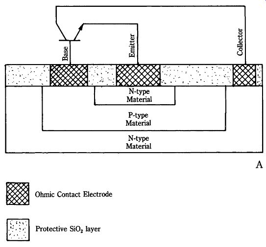
A bipolar transistor is one that uses both types of charge carriers in its operation. In other words, both electrons and holes are used for conduction, meaning that both N-type and P-type materials are needed. Figure 22-20 shows the basic structure of a bipolar transistor. In this case, the device uses two N-type regions and a single P-type region, thereby forming an NPN device. A PNP device has exactly the opposite arrangement. Because NPN devices predominate in the microwave world, however, we will consider only that type of device. Silicon bipolar NPN devices have been used in the microwave region up to about 4 GHz. At higher frequencies, designers typically use field-effect transistors.
The first transistors were of the point-contact type of construction in which "cat's whisker" metallic electrodes were placed in rather delicate contact with the semiconductor material. A marked improvement soon became available in the form of the dif fused junction device. In those devices, N- and P-type impurities are diffused into the raw semiconductor material. Metallization methods are used to deposit electrode con tact pads onto the surface of the device. Mesa devices use a growth technique to build up a substrate of semiconductor material into a table-like structure.
22-20 NPN bipolar transistor.
22-21 (A) Details of planar construction, (B) epitaxial construction, (C)
doping profile, and (D) SICOS construction.
22-21 Continued.
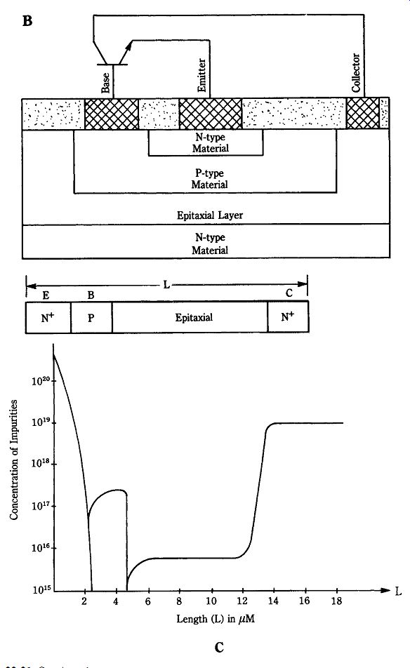
Modern silicon bipolar transistors tend to be NPN devices of either planar (Fig. 22-21A) or epitaxial (Fig. 22-21B) design. The planar transistor is a diffusion device on which surface passivation is provided by a protective layer of silicon dioxide (SiO2). The layer provides protection of surfaces and edges against contaminants migrating into the structure.
The epitaxial transistor (Fig. 22-21B) uses a thin, low-conductivity "epitaxial layer" for part of the collector region (the remainder of the collector region is high-conductivity material). The epitaxial layer is laid down as a condensed film on a substrate made of the same material. Figure 22-21C shows the doping profile versus length for an epitaxial device. Notice that the concentration of impurities, hence region conductivity, is extremely low for the epitaxial region.
The sidewall contact structure (SICOS) transistor is shown in Fig. 22-21D. Regular NPN transistors exhibit a high junction capacitance and a relatively large electron flow across the sub-emitter junction to the substrate. These factors reduce the maximum cutoff frequency and available current gain. A SICOS device with a 0.5-_m base width offers a current gain (Hfe) of 100 and a cutoff frequency of 3 GHz.
Heterojunction bipolar transistors (HBT) have been designed with maximum frequencies of 67 GHz on base widths of 1.2 _m; current gains of 10 to 20 are achieved on very small devices and up to 55 for larger base widths. The operation of HBTs depends in part on the use of a thin coating of NA2S . 9H2O material, which reduces surface charge pair recombination velocity. At very low collector currents, a device with a 0.15-_m base width and 40-_m _ 100-ohmm emitter produced current gains in excess of 3800, with 1500 being also achieved at larger collector currents (on the order of 1 mA/cm2). Compare with non-HBT devices which typically have gain figures under 100.
The Johnson relationships
Microwave bipolar transistors typically obey a set of equations called the Johnson relationships. A set of six equations are useful for determining device limitations.
NOTE: In the following equations, terms are defined when first used; subsequent uses are not redefined.
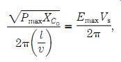
Equation 1: Voltage-frequency limit:
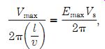
(22-10)
where.... Vmax _ the maximum allowable voltage (EmaxLmin) Vs _ the material saturation velocity Emax _ the maximum electric field (l/v) _ the average charge carrier time at average charge velocity through the length of the material.
Equation II: Current-frequency limit:
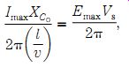
(22-11) where.......
Imax _ the maximum device current XCo _ the reactance of the output capacitance (i.e., 1/(2_(l/v)Co).
Equation III: Power-frequency limit:
(22-12)
where........ Pmax is the maximum power.
Equation IV: Power gain-frequency limit:
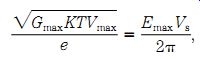
(22-13)
where.......... Gmax _ the maximum power gain K _ Boltzmann's constant (1.38 _ 10^23) T _ the temperature in degrees Kelvin e _ the electronic charge (1.6 _ 10^19).
Equation V: Maximum gain:
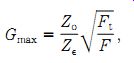
(22-14)
where........
F _ the operating frequency Zo _ the real component of output impedance Zin _ the real component of the input impedance.
Equation VI: Impedance ratio:
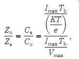
(22-15)
where........
Cin = the input capacitance
Co = the output capacitance
Tb = charge transit time.
Cutoff frequency (Ft)
The cutoff frequency (Ft) is the frequency at which current gain drops to unity.
Several factors affect cutoff frequency. First, the saturation velocity for charge carriers in the semiconductor material; second is the time required to charge the emitter-base junction capacitance (Teb); third, the time required to charge the base collector junction capacitance (Tcb); fourth, the base region transit time (Tbt); and fifth, base-collector depletion zone transit time (Tbc). These times add together to give us the emitter-collector transit time (T). The expression for cutoff frequency is:
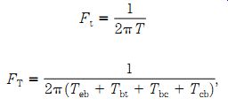
(22-16) or (22-17)
where.........
Ft is the frequency in hertz (Hz)
Times are in seconds.
Bipolar transistor geometry
Two of the problems that limited the high-frequency performance of early transistors were emitter and base resistances and base transit time. Unfortunately, simply reducing the base width in order to improve transit time, and reduce overall resistance, also reduces current and voltage-handling capability. Although some improvements were made, older device internal geometries were clearly limited. The solutions to these problems lay in the geometry of the base-emitter junction. Figure 22-22 shows three geometries that yielded success in the microwave region: inter digital (Fig. 22-22A), matrix (Fig. 22-22B), and overlay (Fig. 22-22C). These construction geometries yielded the thin, wide-area, low-resistance base regions that are needed to increase the operating frequency.
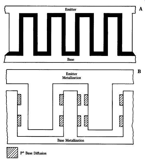
22-22 (A) Inter-digital emitter construction, (B) matrix construction, and
(C) overlay construction.
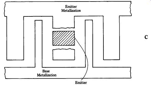
22-22 Continued.
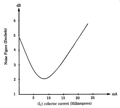
22-23 Noise figure vs collector current.
Low-noise bipolar transistors
Geometries that provide the low resistance needed to increase operating frequency also serve to reduce the noise generated by the device. There are three main contributors to noise in a bipolar transistor: thermal noise, shot noise in the e-b circuit, and shot noise in the b-c circuit. The thermal noise is a function of temperature and base region resistance. By reducing the resistance (a function of internal geometry), we also reduce the noise. The shot noise produced by the P-N junction is a function of the junction current. There is an optimum collector current (Ico) at which noise figure is best. Figure 22-23 shows noise figure in decibels plotted against the collector current for a particular device. The production of optimum noise figure at practical collector currents is a function of junction efficiency.
Field-effect transistors
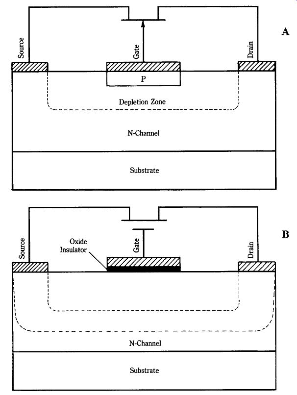
Now look at the field-effect transistor (FET), as used in microwave systems. The FET operates by changing the conductivity of a semiconductor "channel" by varying the electric field in the channel. Two elementary types are found: junction field effect transistors (JFET) and metal-oxide semiconductor field-effect transistors (MOSFET), also sometimes called by the name insulated-gate field-effect transistor (IGFET). In the microwave world, a number of devices are either adaptations or modifications of these basic types.
Figure 22-24A shows the structure of a "generic" JFET device that works on the depletion principle. The channel in this case in N-type semiconductor material and the gate is made of P-type material. A gate-contact metallized electrode is deposited over the gate material. In normal operation, the PN junction is reverse-biased and the applied electric field extends to the channel material.
The electric field repels charge carriers (in this example, electrons) in the channel, creating a depletion zone in the channel material. The wider the depletion zone, the higher the channel resistance. Because the depletion zone is a function of applied gate potential, the gate potential tends to modulate channel resistance. For a constant drain-source voltage, varying the channel resistance also varies the channel current. Because an input voltage varies an output current (Io /Vin), the FET is called a transconductance amplifier. The MOSFET (Fig. 22-24B) replaces the semiconductor material in the gate with a layer of oxide insulating material. Gate metallization is overlaid on the insulator. The electric field is applied across the insulator in the manner of a capacitor. The operation of the MOSFET is similar to the JFET in broad terms and in a depletion-mode device the operation is very similar. In an enhancement-mode device channel resistance drops with increased signal voltage.
Microwave FETs
22-24 (A) JFET transistor and (B) MOSFET transistor.
22-25 MESFET transistor.
The microwave field-effect transistor represented a truly giant stride in the performance of semiconductor amplifiers in the microwave region. Using Group III-A materials, notably gallium arsenide (GaAs), the FET presses cutoff frequency performance way beyond the 3- or 4-GHz limits achieved by silicon bipolar devices.
The gallium arsenide field-effect transistor (GaAsFET) offers superior noise performance (noise figure less than 1 dB is achieved!) over silicon bipolar devices, improved temperature stability, and higher power levels. The GaAsFET can be used as a low-noise amplifier (LNA), class-C amplifier, or oscillator. GaAsFETs are also used in monolithic microwave integrated circuits (MIMIC), extremely high-speed analog-to-digital (A/D) converters, analog/RF applications, and in high-speed logic devices. In addition to GaAs, AlGaAs and InGaAsP materials are also used.
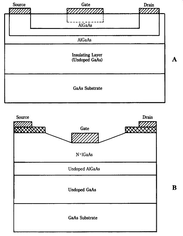
Figure 22-25 shows the principal player among microwave field-effect transistors: the metal semiconductor field-effect transistor (MESFET), also called the Schottky barrier transistor (SBT) or Schottky barrier field-effect transistor (SBFET). The epitaxial "active layer" is formed of N-type GaAs doped with either sulfur or tin ions, with a gate electrode formed of evaporated aluminum. The source and drain electrodes are formed of gold germanium (AuGe) or gold telluride (AuTe) or AuGeTe alloy. Another form of microwave JFET is the high-electron mobility transistor (HEMT), shown in Figs. 22-26A and 22-26B. The HEMT is also known as the two-dimensional electron GaAsFET (TEGFET) and heterojunction FET (HFET). Devices in this category produce power gains up to 11 dB at 60 GHz and 6.2 dB at 90 GHz. Typical noise figures are 1.8 dB at 40 GHz and 2.6 dB at 62 GHz. Power levels at 10 GHz have approached 2 W (CW)/mm of emitter periphery dimension ("emitter" is the gate structure junction in JFET-like devices).
HEMT devices are necessarily built with very thin structures in order to reduce transit times (necessary to increasing frequency because of the 1/T relationship).
These devices are built using ion implantation, molecular beam epitaxy (MBE), or metal organic chemical vapor deposition (MOCVD). The power output capability of field-effect transistors has climbed rapidly over the past few years. Devices in the 10 GHz region have produced 2-W/mm power densities and output levels in the 4- to 5-W region. Figure 22-27 shows a typical power FET internal geometry used to achieve such levels.
An advantage of FETs over bipolar devices is that input impedance tends to be high and relatively frequency-stable. It is thus easier to design wideband power amplifiers and either fixed or variable-frequency (tunable) power amplifiers.
Noise performance
22-26 (A) HEMT transistor and (B) HFET transistor.
Only a few years ago, users of transistors in the high-UHF and microwave regions had to contend with noise figures in the 8- to 10-dB range. A fundamental truism states that no signal below the noise level can be detected without sophisticated computer signals processing (which takes time). Thus, reducing the noise floor of an amplifier helps greatly in building more sensitive real-time microwave systems.
Figure 22-27 shows the typical range of noise figures in decibels expected from various classes of transistors. The silicon bipolar transistor shows a flat noise figure (curve A) up to a certain frequency and a sharp increase in noise thereafter. The microwave FET (curve B), on the other hand, shows increases in both high- and low frequency regions. The same is also true for the HEMT (curve C), but to a lesser degree. Only the supercooled (_260_C!) HEMT performs better.
22-27 Power FET structure.
Most MESFET and HEMT devices show increases in noise at low frequencies.
Some such devices also tend to become unstable at those frequencies. Thus, microwave and UHF devices might, contrary to what your instincts might suggest, fail to work at frequencies considerably below the optimum design frequency range.
Selecting transistors
The criteria for selecting bipolar or field-effect transistors in the microwave range depends on application. The importance of noise figure, for example, becomes apparent in the "front end" of a microwave satellite receiver system. In other applications, power gain and output might be more important. Obviously, gain and noise figure are both important-especially in the front ends of receiver systems. For ex ample, earth communications or receiver terminals typically use a parabolic dish antenna with a low-noise amplifier ("LNA") at the feedpoint. When selecting devices for such applications, however, beware of seemingly self-serving transistor specification data sheets. For example, consider the noise figure specification. As you saw in Fig. 22-28, there is a strong frequency dependence regarding noise figure. Yet de vice data sheets often list the maximum frequency and minimum noise figure-even though the two rarely coincide with one another! When selecting a device, consult the NF-vs-F curve.
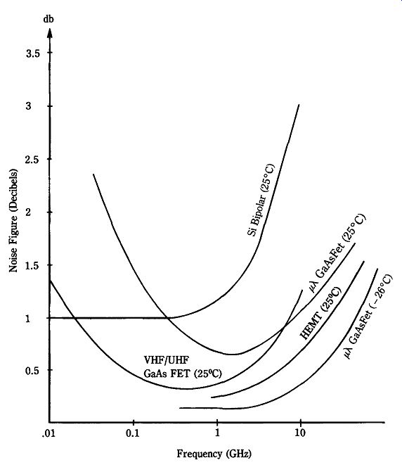
22-28 Noise figure vs frequency for several devices.
Device gain can also be specified in different ways, so caution is in order. There are at least three ways to specify gain: maximum allowable gain (Gmax), gain at optimum noise figure (GNF), and the insertion gain. The maximum obtainable gain occurs usually at a single frequency where the input and output impedances are conjugately matched (i.e., reactive part of impedance canceled out and resistive part transformed for maximum power transfer). The noise figure gain is an impedance matching situation in which noise figure is optimized, but not necessarily power gain.
Rarely, perhaps never, are the two gains the same.
Another specification to examine is the 1-dB compression point. This critical point is that at which a 10-dB increase in the input signal level results in a 9-dB increase in the output signal level. Operation too near this point can cause distortion in a linear amplifier, so it must be avoided.
UHF/microwave RF integrated circuits
Very wideband amplifiers (i.e., those operating from near-dc to UHF or into the microwave regions) have traditionally been very difficult to design and build with consistent performance across the entire passband. Many such amplifiers have either gain irregularities, such as "suck-outs" or peaks. Others suffer large variations of input and output impedance over the frequency range. Still others suffer spurious oscillation at certain frequencies within the passband. Barkhausen's criteria for oscillation requires loop gain of unity or more and 360 deg (in phase) feedback at the frequency of oscillation. At some frequency, the second of these criteria might be met by adding the normal 180 deg phase shift inherent in the amplifier to phase shift be cause of stray RLC components. The result will be oscillation at the frequency where the RLC phase shift was an additional 180 deg. In addition, in the past, only a few applications required such amplifiers. Consequently, such amplifiers were either very ex pensive or didn't work nearly as well as claimed. Hybrid Microwave Integrated Circuit (HMIC) and Monolithic Microwave Integrated Circuit (MMIC) devices were low-cost solutions to the problem.
What are HMICs and MMICs?
MMICs are tiny "gain block" monolithic integrated circuits that operate from dc or near dc to a frequency in the microwave region. HMICs, on the other hand, are hybrid devices that combine discrete and monolithic technology. One product (Signetics NE-5205) offers up to _20 dB of gain from dc to 0.6 GHz, and another low cost device (Mini-circuits Laboratories, Inc. MAR-x) offers _20 dB of gain over the range from dc to 2 GHz, depending on the model. Other devices from other manufacturers are also offered, and some produce gains to _30 dB and frequencies to 18 GHz. Such devices are unique in that they present input and output impedances that are a good match to the 50 or 75 ohm normally used as system impedances in RF circuits.
Monolithic integrated circuit devices are formed through photo-etching and dif fusion processes on a substrate of silicon or some other semiconductor material.
Both active devices (such as transistors and diodes) and some passive devices can be formed in this manner. Passive components, such as on-chip capacitors and resistors, can be formed using various thin- and thick-film technologies. In the MMIC device, interconnections are made on the chip via built-in planar transmission lines.
Hybrids are a level closer to regular discrete circuit construction than ICs. Passive components and planar transmission lines are laid down on a glass, ceramic, or other insulating substrate by vacuum deposition or other methods. Transistors and unpackaged monolithic "chip dies" are cemented to the substrate and then connected to the substrate circuitry via mil-sized gold or aluminum bonding wires.
Because the material in this series could sometimes apply to either HMIC or MMIC devices, the convention herein shall be to refer to all devices in either subfamily as Microwave Integrated Circuits (MIC), unless otherwise specified.
Three things specifically characterize the MIC device. First is simplicity. As you will see in the circuits that follow, the MIC device usually has only input, output, ground, and power supply connections. Other wideband IC devices often have up to 16 pins, most of which must be either biased or capacitor-bypassed. The second feature of the MIC is the very wide frequency range (dc-GHz) of the devices. And the third is the constant input and output impedance over several octaves of frequency.
Although not universally the case, MICs tend to be unconditionally stable be cause of a combination of series and shunt negative feedback internal to the device.
The input and output impedances of the typical MIC device are a close match to either 50 or 75 ohm , so it is possible to make a MIC amplifier without any impedance matching schemes-a factor that makes it easier to broadband than if tuning was used. A typical MIC device generally produces a standing wave ratio (SWR) of less than 2:1 at all frequencies within the passband, provided that it is connected to the design system impedance (e.g., 50-ohm ). The MIC is not usually regarded as a low noise amplifier (LNA), but it can produce noise figures (NF) in the 3- to 8-dB range.
Some MICs are LNAs, however, and the number available should increase in the near future.
Narrowband and passband amplifiers can be built using wideband MICs. A narrowband amplifier is a special case of a passband amplifier and is typically tuned to a single frequency. An example is the 70 MHz IF amplifier used in microwave receivers. Because of input and/or output tuning, such an amplifier will respond only to signals in the 70 MHz frequency band.
Very wideband amplifiers
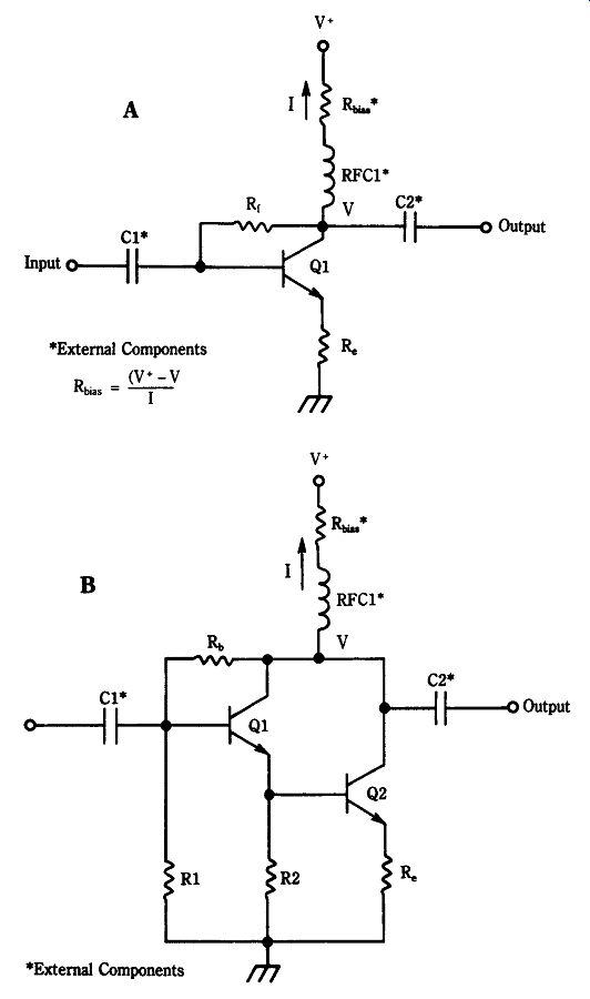
Engineering wideband amplifiers, such as those used in MIC devices, seems simple but has traditionally caused a lot of difficulty for designers. Figure 22-29A shows the most fundamental form of MIC amplifier; it is a common-emitter NPN bipolar transistor amplifier. Because of the high-frequency operation of these devices, the amplifier in MICs are usually made of a material such as gallium arsenide (GaAs). In Fig. 22-29A, the emitter resistor (Re) is unbypassed so introduces a small amount of negative feedback into the circuit. Resistor Re forms series feedback for transistor Q1. The parallel feedback in this circuit is provided by collector-base bias resistor Rf.
Typical values for Rf are in the 500-ohm range and for Re are in the 4- to 6-ohm range. In general, the designer tries to keep the ratio Rf /Re high in order to obtain higher gain, higher output power compression points, and lower noise figures. The input and out put impedances (Ro) are equal and are defined by the patented equation:

(22-18)
where........
Ro = the output impedance in ohms
Rf = the shunt feedback resistance in ohms
Re = the series feedback resistance in ohms.
22-29 (A) Simple wideband RF amplifier, (B) Darlington cascade circuit,
and (C) generic MIC amplifier.
22-29 Continued.
A more common form of MIC amplifier circuit is shown in Fig. 22-29B. Although based on the Darlington amplifier circuit, this amplifier still has the same sort of series and shunt feedback resistors (Re and Rf) as the previous circuit. All resistors except Rbias are internal to the MIC device. A Darlington amplifier, also called a Darlington pair or super-beta transistor, consists of a pair of bipolar transistors (Q1 and Q2) connected so that Q1 is an emitter follower driving the base of Q2, and with both collectors connected in parallel with each other. The Darlington connection permits both transistors to be treated as if they were a single transistor with higher-
than-normal input impedance and a beta gain ( ) equal to the product of the individual beta gains. For the Darlington amplifier, therefore, the beta (or Hfe) is:
o _ ( Q1 )( Q2),

(22-19)
where
o _ the beta gain of the Q1/Q2 pair
Q1
_ the beta gain of Q1
Q2
_ the beta gain of Q2.
You should be able to see two facts. First, the beta gain is very high for a Darlington amplifier that is made with relatively modest transistors. Second, the beta of a Darlington amplifier made with identical transistors is the square of the common beta rating.
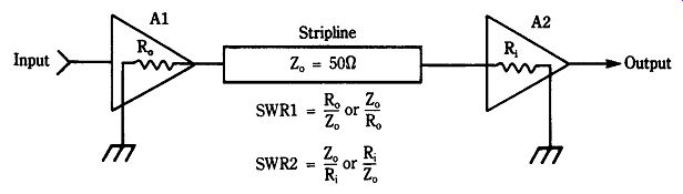
External components
Figures 22-29A and 22-29B show several components that are usually external to the MIC device. The bias resistor (Rbias) is sometimes internal, although on most MIC devices it is external. RF choke RFC1 is in series with the bias resistor and is used to enhance operation at the higher frequencies; RFC1 is considered optional by some MIC manufacturers. The reactance of the RF choke is in series with the bias resistance and increases with frequency according to the 2pFL rule. Thus, the transistor sees a higher impedance load at the upper end of the passband than at the lower end. Use of RFC1 as a "peaking coil" thus helps overcome the adverse effect of stray circuit capacitance that ordinarily causes a similar decreasing frequency dependent characteristic. A general rule is to make the combination of Rbias and XRFC1 form an impedance of at least 500 W at the lowest frequency of operation. The gain of the amplifier might drop about 1 dB if RFC1 is deleted. This effect is caused by the bias resistance shunting the output impedance of the amplifier. The capacitors are used to block dc potentials in the circuit. They prevent intracircuit potentials from affecting other circuits as well as potentials in other circuits from affecting MIC operation. More is said about these capacitors later, but for now understand that practical capacitors are not ideal; real capacitors are complex RLC circuits. Although the L and R components are negligible at low frequencies, they are substantial in the microwave region. In addition, the LC characteristic forms a self-resonance that can either "suck out" or enhance gain at specific frequencies. The result is an uneven frequency-response characteristic at best and spurious oscillations at worst.
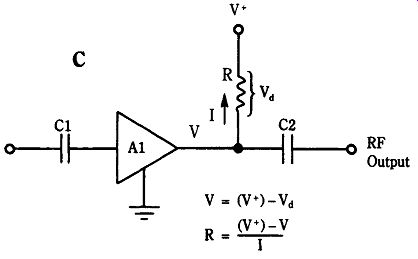
General MMIC amplifier Figure 22-29C shows a "generic" circuit representing MIC amplifiers in general.
As you will see when you look at an actual product, this circuit is nearly complete.
The MIC device usually has only input, output, ground, and power connections;
some models don't have a separate dc power input. There is no dc biasing, no bypassing (except at the dc power line), and no seemingly "useless" pins on the package. MICs use either microstrip packages, like UHF/microwave small-signal transistor packages or small versions of the mini-DIP or metallic IC packages. Some HMICs are packaged in larger transistor-like cases and others are packaged in special hybrid packages. The dc bias resistor (Rbias) connected to either the power supply terminal (if any) or the output terminal must be set to a value that limits the current to the advice and drops the supply voltage to a safe value. MIC devices typically require a low dc voltage (4 to 7 Vdc) and a maximum current of about 15 to 25 mA de pending on the type. There might also be an optimum current of operation for a specific device. For example, one device advertises that it will operate over a range of 2 to 22 mA, but that the optimum design current is 15 mA. The value of resistor needed for Rbias is found from Ohm's law:
(22-20) where.......
Rbias _ in ohms
V__ dc power supply potential in volts
V = rated MIC device operating potential in volts
I_bias = operating current in amperes.
The construction of amplifiers based on MIC devices must follow microwave practices. This requirement means short, wide, low-inductance leads made of printed circuit foil and stripline construction. Interconnection conductors behave like transmission lines at microwave frequencies so they must be treated as such. In addition, capacitors should be capable of passing the frequencies involved, yet have as little inductance as possible. In some cases, the series inductance of common capacitors forms a resonance at some frequency within the passband of the MMIC de vice. These "resonant" circuits can sometimes be detuned by placing a small ferrite bead on the capacitor lead. Microwave "chip" capacitors are used for ordinary by passing.
MIC technology is currently able to provide very low-cost microwave amplifiers with moderate gain and noise figure specifications and better performance is avail able at higher cost; the future holds promise of even greater advances. Manufacturers have extended MIC operation to 18 GHz and have dropped noise figures substantially. In addition, it is possible to build the entire front end of a microwave receiver into a single HMIC or MMIC, including the RF amplifier, mixer, and local oscillator stages.
Although MIC devices are available in a variety of package styles, those shown in Fig. 22-30 are typical of many. Because of the very high-frequency operation of these devices, MICs are packaged in stripline transistor-like cases. The low-inductance leads for these packages are essential in UHF and microwave applications.
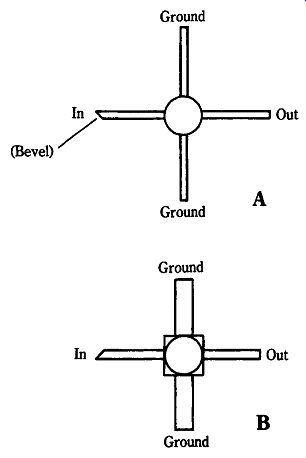
22-30 RF transistor and MIC packages.
22-31 Cascade MIC amplifiers.
Cascade MMIC amplifiers
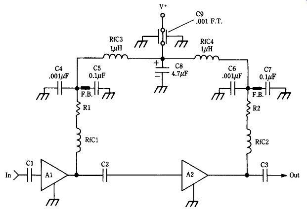
MMIC devices can be connected in cascade (Fig. 22-31) to provide greater gain than is available from only a single device, although a few precautions must be ob served. It must be recognized, for example, that MICs possess a substantial amount of gain from frequencies near dc to well into the microwave region. With all cascade amplifiers, you must prevent feedback from stage to stage. Two factors must be ad dressed. First, as always, is component layout. The output and input circuitry external to the MIC must be physically separated to prevent coupling feedback.
Second, it is necessary to decouple the dc power supply lines that feed two or more stages. Signals carried on the dc power line can easily couple into one or more stages, resulting in unwanted feedback.
Figure 22-31 shows a method for decoupling the dc power line of a two-stage MIC amplifier. In lower-frequency cascade amplifiers, the V_ ends of resistors R1 and R2 would normally be joined together and connected to the dc power supply.
Only a single capacitor would be needed at that junction to ensure adequate decoupling between stages. But as the operating frequency increases, the situation becomes more complex, in part caused by the nonideal nature of practical components. For example, in an audio amplifier the electrolytic capacitor used in the power supply ripple filter might provide sufficient decoupling. At RF frequencies, however, electrolytic capacitors are essentially useless as capacitors (they act more like resistors at those frequencies).
The decoupling system in Fig. 22-31 consists of RF chokes RFC3 and RFC4 and capacitors C4 through C9. The RF chokes help block high frequency ac signals from traveling along the power line. These chokes are selected for a high reactance at VHF through microwave frequencies, while having a low dc resistance. For example, a 1-uH RF choke might have only a few milliohms of dc resistance, but (by 2uFL) has a reactance of more than 3000 _ at 500 MHz. It is important that RFC3 and RFC4 be mounted so as to minimize mutual inductance because of the interaction among their respective magnetic fields.
Capacitors C4 through C9 are used for bypassing signals to ground. Notice that a wide range of values, and several types of capacitors, are used in this circuit. Each has its own purpose. Capacitor C8, for example, is an electrolytic and is used to de couple very low-frequency signals (i.e., those up to several hundred kilohertz).
Because C8 is ineffective at higher frequencies, it is shunted by capacitor C9, shown in Fig. 22-31 as a feedthrough capacitor. Such a capacitor is usually mounted on the shielded enclosure housing the amplifier. Capacitors C5 and C7 are used to bypass signals in the HF region. Because these capacitors are likely to exhibit substantial series inductance, they will form undesirable resonances within the amplifier pass band. Ferrite beads are sometimes installed on each capacitor lead in order to detune capacitor self-resonances. Like C9, capacitors C4 and C6 are used to decouple signals in the VHF-and-up region. These capacitors must be of microwave "chip" construction or they might prove ineffective above 200 MHz or so.
Gain in cascade RF amplifiers In low-frequency amplifiers, you might reasonably expect the composite gain of a cascade amplifier to be the product of the individual stage gains:
(22-21) where G1-Gn _ the gains in decibels.
Although that reasoning is valid for low-frequency voltage amplifiers, it fails for RF amplifiers (especially in the microwave region), where input-output standing wave ratio (SWR) becomes significant. In fact, the gain of any RF amplifier cannot be accurately measured if the SWR is greater than about 1.15:1.
There are several ways in which SWR can be greater than 1:1, and all of them involve an impedance mismatch. For example, the amplifier might have an input or output resistance other than the specified value. This situation can arise because of design errors or manufacturing tolerances. Another source of mismatch is the source and load impedances. If these impedances are not exactly the same as the amplifier input or output impedance, respectively, a mismatch will occur.
An impedance mismatch at either input or output of the single-stage amplifier will result in a gain mismatch loss (M.L.) of:
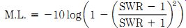
(22-22)
where.....
M.L. _ mismatch loss in decibels (dB)
SWR _ standing wave ratio (dimensionless).
22-32 Strip-line impedance matching between to MICs.
In a cascade amplifier we have the distinct possibility of an impedance mis match, hence an SWR, at more than one point in the circuit. An example (Fig. 22-32) might be where neither the output impedance (Ro) of the driving amplifier (A1) nor the input impedance (Ri) of the driven amplifier (A2) are matched to the 50-ohm (Zo) microstrip line that interconnects the two stages. Thus, Ro/Zo or its inverse forms one SWR, although Ri/Zo or its inverse forms the other. For a two-stage cascade amplifier the mismatch loss is:
(22-23)
The mismatch loss can very from a negative loss resulting in less system gain (Gb) to a "positive loss" (which is actually a gain in its own right), resulting in greater system gain (Ga). The reason for this apparent paradox is that it is possible for a mis matched impedance to be connected to its complex conjugate impedance.
Attenuators in amplifier circuits?
It is common practice to place attenuator pads in series with the input and out put signal paths of microwave circuits to "swamp-out" impedance variations that adversely affect circuits which ordinarily require either impedance matching or a constant impedance. Especially when dealing with devices such as LC filters (low pass, high-pass, and bandpass), VHF/UHF amplifiers, matching networks, and MIC devices, it is useful to insert 1-dB, 2-dB, or 3-dB resistor attenuator pads in the input and output lines. The characteristics of many RF circuits depend on seeing the design impedance at input and output terminals. With the attenuator pad (see Fig. 22-33) in the line, source and load impedance changes don't affect the circuit nearly as much.
The attenuator tactic is also sometimes useful when confronted with seemingly unstable very wideband amplifiers. Insert a 1-dB pad in series with both input and output lines of the unstable amplifier. This tactic will cost about 2 dB of voltage gain, but it often cures instabilities that arise out of frequency-dependent load or source impedance changes.
22-33 Input and output attenuators provide additional stability.
Noise figure in cascade amplifiers
It is common in microwave systems-especially in communications and radar receivers-to place a low-noise amplifier (LNA) at the input of the system. The amplifiers that follow the LNA need not be of LNA design, so they are less costly. The question is sometimes asked: "why not use a LNA in each stage?" The answer can be deduced from Friis' equation:
(22-24)
where.........
(Note: All quantities are dimensionless ratios rather than decibels) NF_total _ system noise figure
NF1
_ noise figure of stage-1
NF2
_ noise figure of stage-2
NFn _ noise figure of stage-nth
G1 _ gain of stage-1
G2 _ gain of stage-2
Gn _ gain of nth stage.
A lesson to be learned from this equation is that the noise figure of the first stage in the cascade chain dominates the noise figure of the combination of stages. Notice that the overall noise figure increased only a small amount when a second amplifier was used.
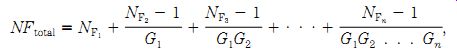
MAR-x series devices (a MIC example)
The Mini-Circuits Laboratories MAR-x series of MIC devices (Fig. 22-34A) offers gains from _13 dB to _20 dB and top-end frequency response of either 1 or 2 GHz de pending on the type. The package used for the MAR-x device (Fig. 22-34B) is similar to the case used for modern UHF and microwave transistors. Pin 1 (RF input) is marked by a color dot and a bevel. The usual circuit for the MAR-x series devices is shown in Fig. 22-34A. The MAR-x device requires a voltage of _5 Vdc on the output terminal and must derive this potential from a dc supply of greater than _7 Vdc.
The RF choke (RFC1) is called optional in the engineering literature on the MAR-x, but it is recommended for applications where a substantial portion of the total bandpass capability of the device is used. The choke tends to pre-emphasize the higher frequencies and thereby overcomes the deemphasis normally caused by circuit capacitance; in traditional video amplifier terminology that coil is called a "peaking coil" because of this action (i.e., it peaks up the higher frequencies).
It is necessary to select a resistor for the dc power supply connection. The MAR x device wants to see _5 Vdc at a current not to exceed 20 mA. In addition, V_ must be greater than _7 V. Thus, you need to calculate a dropping resistor (Rd) of:
(22-25)
where.....
Rd is in ohms.
I is in amperes.
In an amplifier designed for _12-Vdc operation, you might select a trial bias cur rent of 15 mA (i.e., 0.015 A). The resistor value calculated is 467 _ (a 470-ohm, 5%, film resistor should be satisfactory). As recommended, a 1-dB attenuator pad is inserted in the input and output lines. The V_ is supplied to this chip through the output terminal.
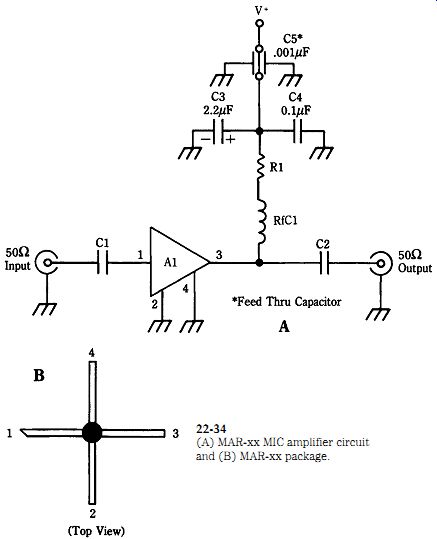
22-34 (A) MAR-xx MIC amplifier circuit and (B) MAR-xx package.
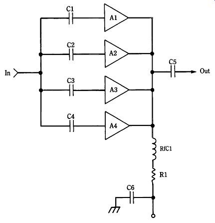
22-35 Parallel MAR-xx devices.
Combining MMIC amplifiers in parallel
Figures 22-35 through 22-37 show several MIC applications involving parallel combinations of MIC devices. Perhaps the simplest of these is the configuration of Fig. 22-35. Although each input must have its own dc-blocking capacitor to protect the MIC device's internal bias network, the outputs of two or more MICs might be connected in parallel and share a common power-supply connection and output coupling capacitor. Several advantages are realized with the circuit of Fig. 22-35.
First, the power output increases even though total system gain (Po/Pm) remains the same. As a consequence, however, drive power requirements also increase. The output power increases 3 dB when two MICs are connected in parallel and 6 dB when four are connected (as shown). The 1-dB output-power compression point also increases in parallel amplifiers in the same manner: 3 dB for two amplifiers and 6 dB for four amplifiers in parallel.
The input impedance of a parallel combination of MIC devices reduces to Ri /N, where N is the number of MIC devices in parallel. In the circuit shown in Fig. 22-35, the input impedance would be Ri/4 _ 12.5 _ if the MICs are designed for 50-ohm service. Because 50/12.5 represents a 4:1 SWR, some form of input impedance matching must be used. Such a matching network can be either broad-banded or frequency-specific as the need dictates. Figures 22-36 through 22-38 show methods for accomplishing impedance matching.
The method shown in Fig. 22-36 is used at operating frequencies up to about 100 MHz and is based on broadband ferrite toroidal RF transformers. These transform ers dominate the frequency response of the system because they are less broad banded than the usual MIC device. This type of circuit can be used as a gain block in microwave receiver IF amplifiers (which are frequently in the 70-MHz region) or in the exciter section of Master Oscillator Power Amplifier (MOPA) transmitters.
22-36 HF/low-band VHF amplifier using broadband toroidal RF transformers
for combining and matching.
Another method is more useful in the UHF and microwave regions. Figure 22-37 shows several forms of the Wilkinson power divider circuit. A LC network version is shown here for comparison, although coaxial or stripline transmission line versions are used more often in microwave applications. The LC version (Fig. 22-37A) is used to frequencies of 150 MHz. This circuit is bidirectional so it can be used as either a power splitter or power divider. RF power applied to port C is divided equally between port A and port B. Alternatively, power applied to ports A/B are summed together and appear at port C. The component values are found from the following relationships:
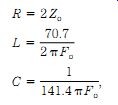
(22-26)

(22-27)
(22-28)
where
R is in ohms
L is in henrys (H)
C is in farads (F)
Fo is in hertz (Hz).
22-37 (A) Wilkinson power divider, (B) coaxial cable version, (C) microstrip
version (end view), and (D) plan view of strip-line version.
Figure 22-37B shows a coaxial-cable version of the Wilkinson divider that can be used at frequencies up to 2 GHz. The lower frequency limit is set by practicality because the transmission-line segments become too long to be handled easily. The upper frequency limit is set by the practicality of handling very short lines and by the dielectric losses, which are frequency dependent. The transmission line segments are each a quarter wavelength; their length is found from:

(22-29)
where L _ the physical length of the line in inches F _ the frequency in megahertz (MHz) V _ the velocity factor of the transmission line (0 to 1) An impedance transformation can take place across a quarter-wavelength trans mission line if the line has a different impedance than the source or load impedances being matched. Such an impedance-matching system is often called a Q- section.
The required characteristic impedance for the transmission line is found from:

(22-30)
where........
(Zo)
_ the characteristic impedance of the quarter-wavelength section
ZL = the load impedance
Zo = the system impedance (e.g., 50-ohm ).
In the case of parallel MIC devices, the nominal impedance at port C of the Wilkinson divider is one-half of the reflected impedance of the two transmission lines. For example, if the two lines are each 50-ohm transmission lines, then the impedance at port C is 50/2 __ 25 _. Similarly, if the impedance of the load (i.e., the reflected impedance) is transformed to some other value, then port C sees the parallel combination of the two transformed impedances. In the case of a parallel MIC amplifier, you might have two devices with 50-ohm input impedance each. Placing these devices in parallel halves the impedance to 25 _, which forms a 2:1 SWR with a 50-ohm system impedance. But if the quarter-wavelength transmission line trans forms the 50-ohm input impedance of each device to 100 ohm, then the port C impedance is 100/2 _ 50-ohm . . . which is correct. At the upper end of the UHF spectrum, and in the microwave spectrum, it might be better to use a stripline transmission line instead of coaxial cable.
A stripline (see Fig. 22-37C) is formed on a printed circuit board. The board must be double-sided so that one side can be used as a ground plane and the stripline is etched into the other side. The length of the stripline depends on the frequency of operation; either half-wave or quarter-wave lines are usually used. The impedance of the stripline is a function of three factors: (1) stripline width (w), (2) height of the stripline above the ground-plane (h), and (3) dielectric constant ( ) of the printed circuit material:

(22-31)
where......
h =the height of the stripline above the groundplane
w = the width of the stripline (h and w in same units)
Zo = the characteristic impedance in ohms.
22-38 General circuit for a multi-MIC amplifier using Wilkinson dividers.
The stripline transmission line is etched into the printed circuit board, as in Fig. 22-37D. Strip-line methods use the printed wiring board to form conductors, tuned circuits, and so on. In general, for microwave operation, the conductors must be very wide (relative to their simple dc and RF power carrying size requirements) and very short in order to reduce lead inductance. Certain elements, the actual strip-lines, are transmission-line segments and follow transmission-line rules. The printed circuit material must have a large permitivity and a low loss tangent. For frequencies up to about 3 GHz, it is permissible to use ordinary glass-epoxy double-sided board ( _ 5), but for higher frequencies, a low-loss material, such as Rogers Duroid ( _ 2.17), must be used.
When soldering connections in these amplifiers, it is important to use as little solder as possible and keep the soldered surface smooth and flat as possible. Other wise, the surface wave on the strip-line will be interrupted-and operation suffers.
Figure 22-38 shows a general circuit for a multi-MIC amplifier based on one of the above discussed Wilkinson power dividers. Because the divider can be used as either splitter or combiner, the same type can be used as input (WD1) and output (WD2) terminations. In the case of the input circuit, port C is connected to the amplifier main input and ports A/B are connected to the individual inputs of the MIC devices. At the output circuit, another divider (WD2) is used to combine power out put from the two MIC amplifiers and direct it to a common output connection. Bias is supplied to the MIC amplifiers through a common dc path at port C of the Wilkin son dividers.