AMAZON multi-meters discounts AMAZON oscilloscope discounts
One of the things that fascinated people about radio from its very earliest days is that signals arrive seemingly by magic through the air from long distances. It was very quickly discovered that radio signals are electromagnetic waves--exactly like light and infrared, except for frequency and wavelength. Radiowave have a much lower frequency than light; therefore, the wavelengths are much longer. The wavelengths of radio signals range from around 25,000 m at the low-VLF range down to millimeters in the upper microwave spectrum.
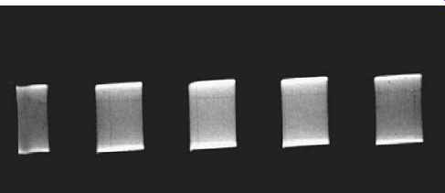
FIG. 1 CW signal.
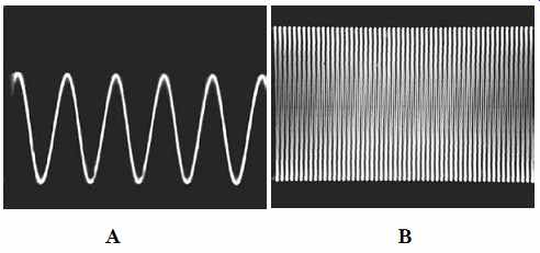
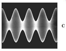
FIG. 2 (A) Audio modulating signal; (B) RF carrier; and (C) AM signal.
Consider three different forms of signals: continuous wave (CW), amplitude modulation (AM), and frequency modulation (FM). The CW signal is only considered very briefly because it is largely irrelevant to most readers of this guide. The CW signal (Fig. 1) is made up of sinusoidal oscillations at the transmitter frequency.
For example, a 500-kHz maritime signal oscillates 500,000 times per second. The critical point about the CW signal is that it has a constant amplitude while it is on. If the signal is turned on and off, to form dots and dashes of the Morse code, it is possible to send messages with the CW signal. This type of signal was transmitted by ships at sea during the early days of wireless . . . and indeed maritime radiotelegraph CW is still heard on the air today (even though less and less--The U.S. Coast Guard has stopped monitoring 500 kHz).
Modulation is the act of adding information to an unmodulated radio signal (called the carrier). That unmodulated signal is, by the way, the same as an unkeyed CW signal. The modulating signal is usually audio from speech or music sources. In radio, the technical term for the modulating signal is intelligence, although considering the content of certain talk shows, the Citizen's Band, and other radio transmissions, it is difficult to keep a straight face when talking about the modulating signal as "intelligence." Fig. 2 shows the relationship between the modulating signal (Fig. 2A), the carrier (Fig. 2B), and the resultant amplitude-modulated signal (Fig. 2C).
The transmitter modulator stage superimposes the audio signal onto the carrier, resulting in the characteristic signal shown in Fig. 2C. This signal is received at the radio set. Notice that the peaks of the AM signal vary in step with the audio modulating signal. The frequency of the AM carrier remains constant, but its intensity or amplitude varies with the audio signal. In this case, the frequency or phase of the carrier varies in step with the audio signal, and the amplitude remains constant.
The tuner
The airspace surrounding the radio is filled with a cacophony of electromagnetic signals that are ready for the plucking. Very early in the radio business, it was found that radios not only worked better with tuning units but would separate signals on different wavelengths (frequencies). The standard radio tuner consists of an inductor and a capacitor. Fig. 3 shows an RF tuner circuit. An inductor stores energy in a surrounding magnetic field, and the capacitor stores energy in an electrostatic field between the two plates.
Inductors and capacitors both provide some opposition to the flow of ac current (including radio frequency or "RF" frequencies). This opposition is called reactance and for inductors it is inductive reactance (XL); for capacitors, it is called capacitive reactance (XC). At a certain frequency, called resonance, these two reactances are equal (XL = XC). When this occurs (in the LC "tank" circuit), the electrostatic field of the capacitor and the magnetic field oscillate so that energy is swapped back and forth between the fields of the inductor and capacitor. The tuner will accept this frequency but reject others. The resonant frequency of the LC "tank" circuit of Fig. 3 is given by:
F _ 1 2_1LC , 5-3(eqn. 1)
where f is the frequency in hertz (Hz)
L is the inductance in henrys (H)
C is the capacitance in farads (F).
Parallel-resonant LC circuit.
Radio tuners don't normally use the simple LC resonant tank circuit of Fig. 3 but rather depend on the RF transformer principle shown in Fig. 4. The primary winding of the RF transformer (L1A) consists of a few turns of wire wound on the lower end of the same coil form as the main tuning coil, L1B.
If either the inductor or capacitor is made variable, then an operator can select from a number of resonant frequencies by varying the frequency of the tuned circuit.
In most radios, the tuner control is a variable capacitor because of the ease with which these components can be made.
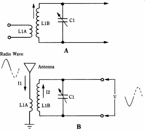
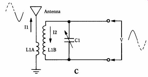
FIG. 4 (A) Link-coupled RF transformer LC-tuned circuit; (B) antenna coupler
circuit using Fig. 2A circuit on one half of incoming signal; and (C)
same circuit on alternate half-cycle (note current direction reversal).
When the radiowave is captured by the antenna, a small current (I1) at the same frequency as the radiowave is set up in the antenna-ground path. One-half of the radiowave causes the current to flow toward the ground (Fig. 4B). Because the primary (L1A) and secondary (L1B) are magnetically coupled, current I1 induces current I2, which flows in the LC tank circuit producing a signal voltage (V) across the out put terminals. Similarly, when the radiowave reverses polarity, the antenna-ground current also reverses direction (Fig. 4C). The current in the secondary is also therefore reversed, creating the other half of the output signal voltage (V). As the radiowave oscillates between its peaks at the radio transmitter frequency, the cur rents (I1 and I2) and signal voltage (V) also oscillate at the same frequency. Only the resonant frequency oscillates efficiently in the LC tank circuit, so only it will appear at the output terminals-even though many waves set up currents in the antenna-ground circuit.
As a point of interest, even though most radio tuners use a fixed inductor and a variable capacitor (which is ganged to the tuning knob on the radio front panel), a few models out there used a fixed capacitor and a variable inductor (Fig. 5). The coil has a hollow coil form and is tuned with a powdered-iron or ferrite core that is connected to the tuning dial through a dial cord. These radios were produced during World War II, when the metal needed to make a variable capacitor was far too precious to the war effort for use in consumer radios. Also, some very high-quality commercial and military receivers used permeability (i.e., inductor) tuning mechanisms; car radios also typically used PTM assemblies in the days before all-electronic tuning.
The selectivity of the radio is its ability to separate stations adjacent to each other on the dial. The number of LC-tuned circuits in the signal path determines the selectivity. Fig. 6 shows the curves to expect with one tuned circuit (A), two tuned circuits (B), and three tuned circuits (C). Notice that in each case, the LC tuned circuit does not pick out only one single frequency, but rather it picks up a small band of frequencies that surround the resonant frequency.
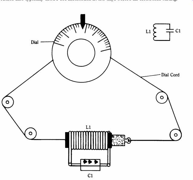
FIG. 5 Inductor-tuned radio tuning circuit was common in World War II consumer
and military "morale" radio receivers.
The selectivity of the receiver is measured in terms of the bandwidth of the tuned circuit. The standard method for specifying selectivity is to measure the frequency response of the circuit to find the points where the power drops -3 dB or the voltage drops -6 dB (same point, but specified differently). Fig. 7 shows the response of a moderately selective LC tank circuit. The bandwidth is the frequency difference F2 - F1, where F1 and F2 are the frequencies at which the response drops -6 dB (voltage), or -3 dB (power), from the level found at resonant frequency, FR.
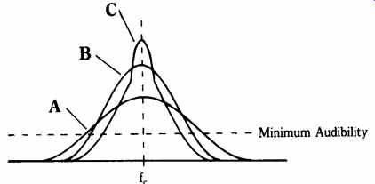
FIG. 6 Bandwidth effects of three different coupling schemes.
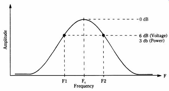
FIG. 7 Bandpass characteristics.
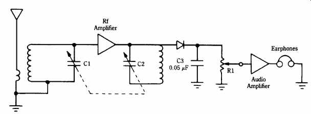
FIG. 8 Simple TRF radio receiver.
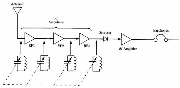
FIG. 9 Multistage TRF radio receiver.
Tuned radio-frequency (TRF) receivers
The tuned radio frequency (TRF) radio uses one or more radio frequency (RF) amplifiers to boost the weak signal received from the antenna. The simplest form of TRF radio (Fig. 8) consists of a single RF amplifier stage, with frequency selection (LC tank) circuits at the input and output. The signal at the antenna input of the RF amplifier is very weak, but because of the amplification of the tube in the amplifier, it is boosted to a stronger level at the output.
The RF amplifier is followed by a detector, which is, in turn, followed by an audio amplifier and a reproducer (e.g., loudspeaker). The detector demodulates the RF signal to recover the audio signal that was impressed on the RF carrier at the transmitter. This audio signal is boosted to a higher power level in the audio frequency (AF) amplifier and is then fed to a loudspeaker, earphones, or other audio reproducer.
More complex TRF radios will use two or more RF amplifiers in cascade (Fig. 9) prior to the detector and AF amplifier. The extra amplification boosts the signal level even higher than is possible in the single-stage version. Also, the additional tuned circuits tend to sharpen the selectivity quite a bit. If a single tuning shaft operates all of the variable capacitors, i.e., the capacitors are ganged together (as shown by the dotted line in Fig. 9), then "single-knob" operation is possible.
Superheterodyne receivers
The superheterodyne radio receiver (Fig. 10) was invented in the early 1920s, but only a very few sources could supply them because of patent restrictions. Later, however, patents were pooled as the radio industry grew and eventually the patents expired. The superheterodyne design was so superior that within a decade it took over all but a very few radios and is still today the basic design of all AM and FM radio receivers.
The block diagram to a superheterodyne receiver is shown in Fig. 10. The basic idea of the superheterodyne is to convert all the RF carrier signals from the radio waves to a fixed frequency, where it can be amplified and otherwise processed. The stages of the basic superheterodyne receiver consists of a mixer, a local oscillator (LO), an intermediate frequency (IF) amplifier, a detector, and an AF amplifier. The latter two stages are also used in TRF radios and serve exactly the same function in superheterodynes. Better-quality superhet radios also include an RF amplifier.
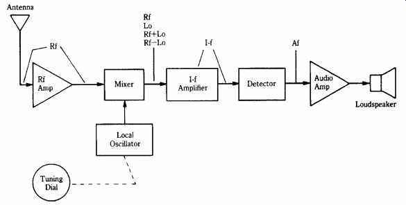
FIG. 10 Block diagram to a superheterodyne receiver.
The RF amplifier boosts the weak signal from the antenna and provides the radio with some additional selectivity. It also prevents the signal from the LO from being coupled to the antenna, where it could be radiated into space. The RF amplifier is sometimes called the preselector in radio schematics.
The output of the RF amplifier is applied to the input of the mixer stage. Also the input to the mixer is the local oscillator (LO) signal. The two are mixed together in a nonlinear circuit; two produces at least four output frequencies: RF, LO, RF - LO (difference), and RF + LO (sum). Either the sum or difference frequency can be selected for the intermediate frequency (IF), but in the vast majority of antique or classic radios, it was the difference frequency that was used. For AM radios, the IF frequency is 455 or 460 kHz in home radios and 260 or 262.5 kHz in auto radios; FM broadcast receivers and most VHF/UHF monitors use 10.7 MHz as the IF. In many receivers, the LO and mixer are combined into a single stage called a converter. An other name for the mixer or converter is first detector.
The IF amplifier provides the radio with the largest amount of signal gain and the tightest selectivity. It is the fact that the IF operates on only one frequency (e.g., 455 kHz) which permits the very high gain to be achieved without oscillation and other difficulties.
The detector operates at the IF frequency and will demodulate the IF frequency to recover the audio. From the detector, it is passed on to the AF amplifier and the reproducer (speaker).
Using the NE-602/NE-612 chips
The Signetics NE-602A and NE-612 are monolithic integrated circuits containing a double-balanced mixer (DBM), an oscillator, and an internal voltage regulator in a single eight-pin package (Fig. 11). The DBM section operates to 500 MHz, and the internal oscillator section works to 200 MHz. The primary uses of the NE-602 are in HF and VHF receivers, frequency converters, and frequency translators. The de vice can also be used as a signal generator in many popular inductor-capacitor (LC) variable-frequency oscillator (VFO), piezoelectric-crystal (XTAL), or swept frequency configurations. This section explores the various configurations for the dc power supply, the RF input, the local oscillator, and the output circuits. Certain applications of the device are also covered.
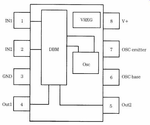
FIG. 11 Internal circuit of NE-602.
The NE-602 version of the device operates over a temperature range of 0 to +70 C, and the SA-602 operates over the extended temperature range of -40 to +85 C. The most common form of the device is probably the NE-602N, which is an eight-pin mini-DIP package. Eight-lead SO surface-mount ("D-suffix") packages are also available. In this section, the NE-602N is featured, although the circuits also work with the other packages and configurations. The improved NE-602AN and NE 602AD are now available.
Because the NE-602 contains both a mixer and a local oscillator, it can operate as a radio receiver "front-end" circuit. It features good noise rejection and reason able third-order intermodulation performance. The noise figure is typically 5 dB at a frequency of 45 MHz. The NE-602 has a third-order intercept point on the order of -15 dBm, referenced to a matched input, although it is recommended that a maximum signal level of -25 dBm (˜3.16 mW) be observed. This signal level corresponds to about 12.6 mV into a 50-ohm load, or 68 mV into the 1500-ohm input impedance of the NE-602. The NE-602 is capable of providing 0.2 uV sensitivity in receiver circuits without external RF amplification. One criticism of the NE-602 is that it appears to sacrifice some dynamic range for high sensitivity-a problem said to be solved in the "A" series (e.g., NE-602AN and in the NE-612).
Frequency conversion or translation
The process of frequency conversion is called heterodyning. When two signals of different frequencies (F1 and F2) are mixed in a nonlinear circuit, a collection of different frequencies will appear in the output of the circuit. These are characterized as F1, F2, and (nF1 +/- mF2), where n and m are integers. In most practical situations, n and m are 1, so the total output spectrum will consist at least of F1, F2, F1 + F2, and F1 - F2. Of course, if the two input circuits contain harmonics, then additional products are found in the output. In superheterodyne radio receivers, either the sum or difference frequency is selected as the intermediate frequency (IF). In order to make the frequency conversion possible, a circuit needs a local oscillator and a mixer circuit (both of which are provided by the NE-602).
The local oscillator (LO) consists of a VHF NPN transistor with the base connected to pin 6 of the NE-602, and the emitter is connected to pin 7; the collector of the oscillator transistor is not available on an external pin. There is also an internal buffer amplifier, which connects the oscillator transistor to the DBM circuit. Any of the standard oscillator circuit configurations can be used with the internal oscillator, provided that access to the collector terminal is not required. Thus, Colpitts, Clapp, Hartley, Butler, and other oscillator circuits can be used with the NE-602 device, and the Pierce and Miller oscillator circuits are not.
The double-balanced mixer (DBM) circuit is shown in Fig. 12; it consists of a pair of cross-connected differential amplifiers (Q1/Q2 with Q5 as a current source; similarly Q3/Q4 with Q6 working as a current source). This configuration is called a Gilbert transconductance cell. The cross-coupled collectors form a push-pull out put (pins 4 and 5) in which each output pin is connected to the V+ power-supply terminal through 1500-ohm resistances. The input is also push-pull and is cross coupled between the two halves of the cell. The local oscillator signal is injected into each cell-half at the base of one of the transistors.
Because the mixer is "double-balanced," it has a key attribute that makes it ideal for use as a frequency converter or receiver front-end: suppression of the LO and RF input signals in the outputs. In the NE-602 chip, the output signals are F1 + F2, and F1 - F2; neither LO nor RF signals appear in the output in any great amplitude. Although some harmonic products appear, many are also suppressed because of the DBM action.
DC power-supply connections on the NE-602 The V+ power-supply terminal of the NE-602 is pin 8, and the ground connection is pin 3; both must be used for the dc power connections. The dc power supply range is +4.5 to +8 Vdc, with a current drain ranging from 2.4 to 2.8 mA.
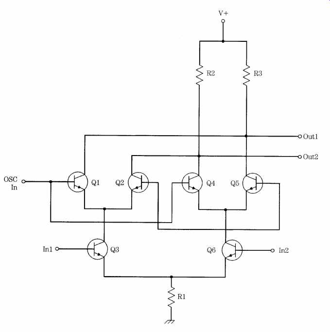
FIG. 12 Transconductance cell double-balanced mixer used in NE-602.
It is highly recommended that the V+ power-supply terminal (pin 8) be by passed to ground with a capacitor of 0.01 to 0.1 uF. The capacitor should be mounted as close to the body of the NE-602 as is practical; short leads are required in radio-frequency (RF) circuits.
Fig. 13A shows the recommended power-supply configuration for situations where the supply voltage is +4.5 to +8 V. For best results, the supply voltage should be voltage-regulated. Otherwise, the local oscillator frequency might not be stable, which leads to problems. A series resistor (˜100 to 180 ohm) is placed between the V+ power supply and the V+ terminal on the NE-602. If the power-supply volt age is raised to +9 V, then increase the value of the series resistance an order of magnitude to 1000 to 1500 ohm (Fig. 13B).
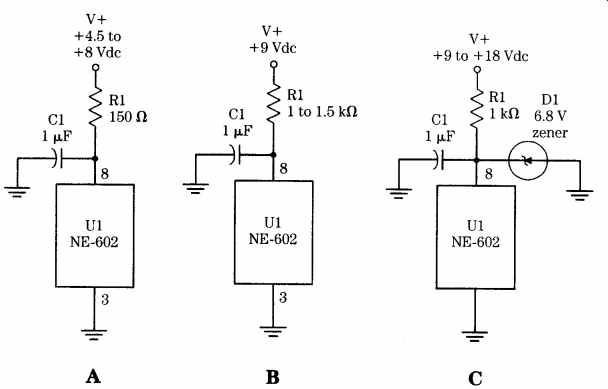
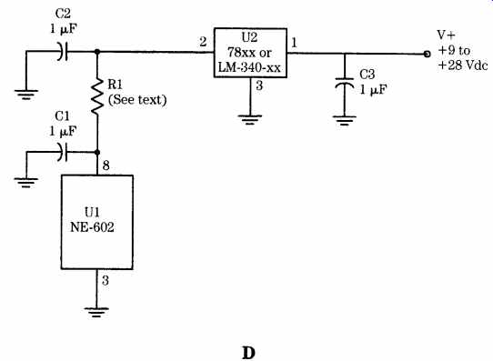
FIG. 13 Dc power supply connections for the NE-602.
If the dc power-supply voltage is either unstable, or is above +9 V, then it is highly recommended that a means of voltage regulation be provided. In Fig. 13C, a zener diode is used to regulate the NE-602 V+ voltage to 6.8 Vdc-even though the supply voltage ranges from +9 to +18 V (a situation found in automotive applications). An alternative voltage regulator circuit is shown in Fig. 13D. This circuit uses a three-terminal IC voltage regulator to provide V+ voltage to the NE-602. Be cause the NE-602 is a very low current drain device, the lower power versions of the regulators (e.g., 78Lxx) can be used. The low-power versions also permit the NE 602 to have its own regulated power supply-even though the rest of the radio receiver uses a common dc power supply. Input voltages of +9 to more than +28 Vdc, depending on the regulator device selected, can be used for this purpose. The version of Fig. 13D uses a 78L09 to provide +9 V to the NE-602, although 78L05 and 78L06 can also be used to good effect.
NE-602 input circuits
The RF input port of the NE-602 uses pins 1 and 2 to form a balanced input. As is often the case in differential amplifier RF mixers, the RF input signals are applied to the base terminals of the two current sources (Q5 and Q6 in Fig. 12). The input impedance of the NE-602 is 1500 ohm, shunted by 3 pF at lower frequencies, although in the VHF region, the impedance drops to about 1000 ohm.
Several different RF input configurations are shown in Fig. 14; both single ended (unbalanced) and differential (balanced) input circuits can be used with the NE-602. In Fig. 14A, a capacitor-coupled, untuned, unbalanced input scheme is shown. The signal is applied to pin 1 (although pin 2 could have been used instead) through a capacitor, C1, that has a low impedance at the operating frequency. The signal level should be less than +25 dBm, or about 68 mV rms (180 mV peak to peak).
Whichever input is used, the alternate input is unused and should be bypassed to ground through a low-value capacitor (0.001 to 0.1 uF, depending on the frequency).
A wideband transformer coupled RF input circuit is shown in Fig. 14B. In this configuration, a wideband RF transformer is connected so that the secondary is applied across pins 1 and 2 of the NE-602, with the primary of the transformer connected to the signal source or antenna. The turns ratio of the transformer can be used to transform the source impedance to 1500 ohm (the NE-602 input impedance).
Either conventional or toroid-core transformers can be used for T1. As in the previous circuit, one input is bypassed to ground through a low-reactance capacitor.
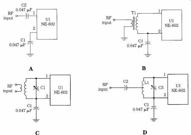
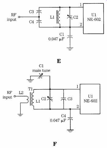
FIG. 14 Input circuits for the NE-602.
Tuned RF input circuits are shown in Figs. 14C-14E and 15. Each of these circuits performs two functions: (a) it selects the desired RF frequency while rejecting others and (b) it matches the 1.5-kOhm input impedance of the NE-602 to the source or antenna system impedance (e.g., 50 ohm). The circuit shown in Fig. 14D uses an inductor (L1) and capacitor (C1) tuned to the input frequency, as do the other circuits, but the impedance matching function is done by tapping the inductor; a dc-blocking capacitor is used between the antenna connection and the coil. A third capacitor, C3, is used to bypass one of the inputs (pin 2) to ground.
Another version of the circuit is shown in Fig. 14E. It is similar in concept to the previous circuit but uses a tapped capacitor voltage divider (C3/C4) for the impedance-matching function. Resonance with the inductor is established by the combination of C1, the main tuning capacitor, in parallel with the series combination of C2 and C3:
(eqn. 2)
The previous two circuits are designed for use when the source or antenna sys tem impedance is less than the 1.5-ohm input impedance of the NE-602. The circuit of Fig. 14F can be used in all three situations: input impedance lower than, higher than, or equal to the NE-602 input impedance-depending on the ratio of the number of turns in the primary winding (L2) to the number of turns in the secondary winding (L1). The situation shown schematically in Fig. 14F is for the case where the source impedance is less than the input impedance of the NE-602.
The secondary of the RF transformer (L1) resonates with a capacitance made up of C1 (main tuning), C2 (trimmer tuning or bandspread), and a fixed capacitor, C3.
An advantage of this circuit is that the frame of the main tuning capacitor is grounded. This feature is an advantage because most tuning capacitors are designed for grounded-frame operation, so construction is easier. In addition, most of the variable-frequency oscillator circuits used with the NE-602 also use a grounded frame capacitor. The input circuit of Fig. 14F can therefore use a single dual-section capacitor for single-knob tuning of both RF input and local oscillator.
Fig. 15 shows a tuned-input circuit that relies, at least in part, on a volt age variable-capacitance ("varactor") diode for the tuning function. The total tuning capacitance that resonates transformer secondary L2 is the parallel combination of C1 (trimmer), C2 (a fixed capacitor), and the junction capacitance of varactor diode, D1. The value of capacitor C3 is normally set to be large compared with the diode capacitance so that it will have little effect on the total capacitance of series combination C3/CD1. In other cases, however, the capacitance of C3 is set close to the capacitance of the diode, so it becomes part of the resonant circuit capacitance.
A varactor diode is tuned by varying the reverse bias voltage applied to the diode. Tuning voltage Vt is set by a resistor voltage divider consisting of R1, R2, and R3. The main tuning potentiometer (R1) can be a single-turn model, but for best resolution of the tuning control use a 10- or 15-turn potentiometer. The fine-tuning potentiometer can be a panel-mounted model for use as a bandspread control or a trimmer model for use as a fine adjustment of the tuning circuit (a function also shared by trimmer capacitor, C1).
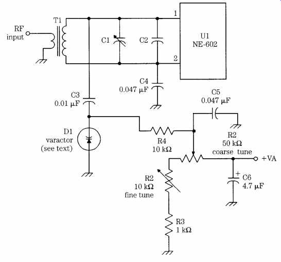
FIG. 15 Varactor-tuned input circuit for NE-602.
The voltage used for the tuning circuit (VA) must be well-regulated, or the tuning will shift with variations of the voltage. Some designers use a separate three terminal IC regulator for VA, but that is not strictly necessary. A more common situation is to use a single low-power 9-V three-terminal IC voltage regulator for both the NE-602 and the tuning network. However, it will only work when the diode needs no more than +9 Vdc for correct tuning of the desired frequency range. Unfortunately, many varactor diodes require a voltage range of about +1 to +37 V to cover the en tire range of available capacitance.
In due course, the oscillator circuits will also show a version of the Fig. 15 circuit that is tuned by a sawtooth waveform (for swept frequency operation) or a digital-to-analog converter (for computer-controlled frequency selection).
NE-602 output circuits
The NE-602 output circuit consists of the cross-coupled collectors of the two halves of the Gilbert transconductance cell (Fig. 12) and are available on pins 4 and 5. In general, it doesn't matter which of these pins is used for the output; in single-ended output configurations, only one terminal is used and the alternate out-put terminal is ignored. Each output terminal is connected internally to the NE-602 to V+ through separate 1.5-kOhm resistors.
Fig. 16A shows the wideband, high-impedance (1.5 kOhm) output configuration.
Either pin 4 or 5 (or both) can be used. A capacitor is used to provide dc blocking.
This capacitor should have a low reactance at the frequency of operation, so values between 0.001 and 0.1 uF are generally selected.
Transformer output coupling is shown in Fig. 16B. In this circuit, the primary of a transformer is connected between pins 4 and 5 of the NE-602. For frequency converter or translator applications, the transformer could be a broadband RF trans former wound on either a conventional slug-tuned form or a toroid form. For direct conversion autodyne receivers, the transformer would be an audio transformer. The standard 1:1 transformers used for audio coupling can be used. These transformers are sometimes marked as impedance ratio rather than turns ratio (e.g., 600 ohm : 600 ohm, or 1.5K:1.5K).
Frequency converters and translators are the same thing, except that the converter terminology generally refers to a stage in a superhet receiver and translator is more generic. For these circuits, the broadband transformer will work, but it is probably better to use a tuned RF/IF transformer for the output of the NE-602. The resonant circuit will reject all but the desired frequency product; e.g., the sum or difference IF frequency. Fig. 16C shows a common form of resonant output circuit for the NE-602. The tuned primary of the transformer is connected across pins 4 and 5 of the NE-602, and a secondary winding (which could be tuned or untuned) is used to couple the signal to the following stages.
A single-ended RF tuned transformer output network for the NE-602 is shown in Fig. 16D. In this coupling scheme, the output terminal of the IC is coupled to the V+ dc power-supply rail through a tuned transformer. Perhaps a better solution to the single-ended problem is the circuit of Fig. 16E. In this circuit, the transformer primary is tapped for a low impedance and the tap is connected to the NE-602 out put terminal through a dc-blocking capacitor. These transformers are easily available in either 455-kHz or 10.7-MHz versions and can also be made relatively easily.
Still another single-ended tuned output circuit is shown in Fig. 16F. In this circuit, one of the outputs is grounded for RF frequencies through a capacitor. Tuning is a function of the inductance of L1 and the combined-series capacitance of C1, C2, and C3. By tapping the capacitance of the resonant circuit at the junction of C2-C3, it is possible to match a lower impedance (e.g., 50 ohm) to the 1.5-kOhm output impedance of the NE-602.
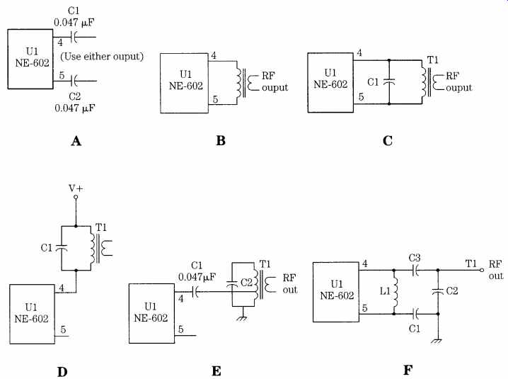
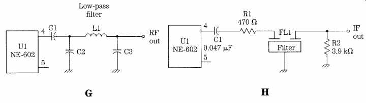
FIG. 16 Output circuits for NE-602.
The single-ended output network of Fig. 16G uses a low-pass filter as the frequency-selective element. This type of circuit can be used for applications, such as a heterodyne signal generator in which the local oscillator frequency of the NE-602 is heterodyned with the signal from another source applied to the RF input pins of the IC. The difference frequency is selected at the output when the low-pass filter is designed so that its cut-off frequency is between the sum and difference frequencies.
In Fig. 16H, an IF filter is used to select the desired output frequency. These filters are available in a variety of different frequencies and configurations, including the Collins mechanical filters that were once used extensively in high-grade communications receivers (262-, 455-, and 500-kHz center frequencies). Current high-grade communications receivers typically used crystal IF filters centered on 8.83, 9, or 10.7 MHz or 455 kHz (with bandwidths of 100 Hz to 30 kHz). Even some broad cast radio receivers use IF filters. Such filters are made of piezo-ceramic material and are usually centered on 260 or 262.5 kHz (AM auto radios), 455 or 460 kHz (other AM radios), or 10.7 MHz (FM radios). The lower-frequency versions are typically made with 4-, 6-, or 12-kHz bandwidths, and the 10.7-MHz versions have bandwidths of 150 to 300 kHz (200 kHz is most common).
In the circuit, Fig. 16H it is assumed that the low-cost ceramic AM or FM filters are used (for other types, compatible resistances or capacitances are needed to make the filter work properly). The input side of the filter (FL1) in Fig. 16H is connected to the NE-602 through a 470-ohm resistor and an optional dc blocking capacitor (C1). The output of the filter is terminated in a 3.9-kOhm resistor. The difference IF frequency resulting from the conversion process appears at this point.
One of the delights of the NE-602 chip is that it contains an internal oscillator circuit that is already coupled to the internal double-balanced mixer. The base and emitter connections to the oscillator transistor inside the NE-602 are available through pins 6 and 7, respectively. The internal oscillator can be operated at frequencies up to 200 MHz. The internal mixer works to 500 MHz. If higher oscillator frequencies are needed, then use an external local oscillator. An external signal can be coupled to the NE-602 through pin 6, but must be limited to less than about -13.8 dBm, or 250 mV, across 1500 Ohm.
The next section shows some of the practical local oscillator (LO) circuits that can be successfully used with the NE-602, including one that allows digital or computer control of the frequency. Oscillator circuits are covered in greater detail in Section 13.