AMAZON multi-meters discounts AMAZON oscilloscope discounts
Low-priced shortwave receivers often suffer from performance problems that are a direct result of the trade-offs that the manufacturers make to produce a low-cost model. In addition, older receivers often suffer the same problems, as do many homebrew radio receiver designs. Chief problems are sensitivity, selectivity, and image response.
Sensitivity is a measure of the receiver's ability to pick-up weak signals. Part of the cause of poor sensitivity is low-gain in the front end of the radio receiver, al though the IF amplifier contributes most of the gain.
Selectivity is a measure of the ability of the receiver to (a) separate two closely spaced signals and (b) reject unwanted signals that are not on or near the desired frequency being tuned. The selectivity provided by a preselector is minimal for very closely spaced signals (that is the job of the IF selectivity in a receiver), but it is used for reducing the effects (e.g., input overloading) of large local signals . . . so fits the second half of the definition.
Image response affects only superheterodyne receivers (which most are) and is an inappropriate response to a signal at twice the receiver IF frequency that the receiver is tuned to. A superhet receiver converts the signal frequency (RF) to an intermediate frequency (IF) by mixing it with a local oscillator (LO) signal generated inside the receiver. The IF can be either the sum or difference between the LO and RF (i.e., LO _ RF or LO _ RF), but in most older receivers and nearly all low-cost receivers it is the difference (LO _ RF). The problem is that there are always two frequencies that meet "difference" criteria: LO _ RF and an image frequency (Fi) that is LO _ IF. Thus, both Fi _ LO and LO _ RF are equal to the IF frequency. If the image frequency gets through the radio's front-end tuning to the mixer, it will appear in the output as a valid signal.
A cure for all of these is a little circuit called an active preselector. A preselector can be either active or passive. In both cases, however, the preselector includes an inductor/capacitor (LC) resonant circuit that is tuned to the frequency that the receiver is tuned to. The preselector is connected between the antenna and the receiver antenna input connector (Fig. 1A). Therefore, it adds a little more selectivity to the front end of the radio to help discriminate against unwanted signals. The inset to Fig. 1A shows the normal switching used in preselectors to allow it to be cut in or out of the circuit.
The difference between the active and passive designs is that the active design contains an RF amplifier stage, but the passive design does not. Thus, the active pre selector also deals with the sensitivity problem of the receiver. This section looks at one passive and several active RF preselector circuits that you can build and adapt to your own needs.
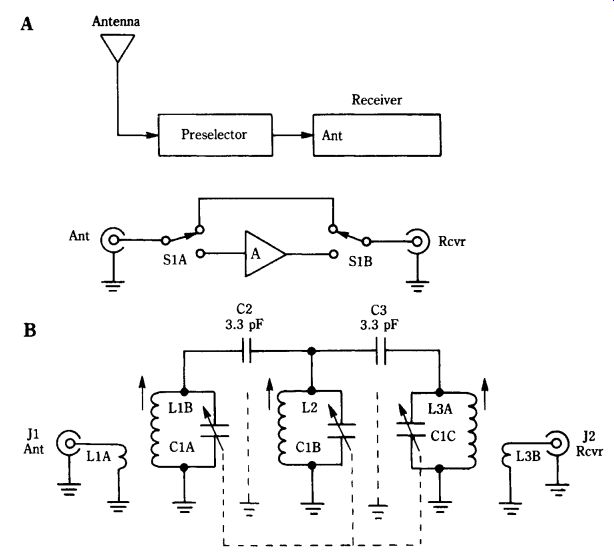
FIG. 1 (A) Preselector is connected as an RF amplifier ahead of the receiver
and (B) passive preselector circuit.
The passive preselector circuit is shown in Fig. 1B. This circuit contains only inductors and capacitors, with each tank circuit shielded from each other. The individual tuned circuits are coupled using the common reactance method (i.e., capacitors C2 and C3 carry RF from one circuit to another). The input coil and the output coil contain link coupling to transfer the RF signal in and out of the circuit respectively.
The tuning capacitors used in the passive preselector should be ganged to a common shaft. A proper unit would have three identical capacitors on the same shaft, with trimmer capacitors on each section (which allows the sections to be aligned to track each other). The trimmer capacitors are adjusted to track the high end of the band, and the slug-tuned inductors are adjusted for low-end tracking.
The active preselector circuits are based on either of two devices: the MPF-102 junction field-effect transistor (JFET) and the 40673 metal-oxide semiconductor field effect transistor (MOSFET). Both of these devices are easily available from both mail order sources and from local distributor replacement lines (for example, the MPF-102 is the NTE-312 and the 40673 is the NTE-222). These transistors were selected be cause they are both easily obtained and are well-behaved into the VHF region.
Preselectors should be built inside shielded metal boxes in order to prevent RF leakage around the device. Select boxes that are either die-cast or are made of sheet metal and have an overlapping lip. Do not use a low-cost tab-fit sheet-metal box.
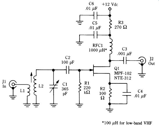
FIG. 2 JFET active preselector circuit.
JFET preselector circuits
Figure 7-2 shows the most basic form of JFET preselector. This circuit will work into the low-VHF region. This circuit is in the common source configuration, so the input signal is applied to the gate and the output signal is taken from the drain. The source bias is supplied by the voltage drop across resistor R2, and the drain load is supplied by a series combination of a resistor (R3) and a radio frequency choke (RFC1). The RFC should be 1000 uH (1 mH) at the AM broadcast band and HF (shortwave), and 100 uH in the low-VHF region (_30 MHz). At VLF frequencies (below the AM broadcast band), use 2.5 mH for RFC1 and increase all 0.01-uF capacitor values to 0.1 uF. All capacitors are either disk ceramic or one of the newer "poly" capacitors (if rated for VHF service-not all are!).
The input circuit is tuned to the RF frequency, but the output circuit is untuned.
The reason for the lack of output tuning is that tuning both the input and the output permits the JFET to oscillate at the RF frequency-and you don't want that. Other possible causes of oscillation include layout and a self-resonance frequency of the RFC that is too near the RF frequency (select another choke).
The input circuit consists of an RF transformer that has a tuned secondary (L2/C1). The variable capacitor (C1) is the tuning control. Although the value shown is the standard 365-pF "AM broadcast variable," any form of variable can be used if the inductor is tailored to it. These components are related by:

, (Eq. 1)
where
F is the frequency in hertz
L is the inductance in henrys
C is the capacitance in farads.
Be sure to convert inductances from microhenrys to henrys and picofarads to farads. Allow approximately 10 pF to account for stray capacitances, although keep in mind that this number is a guess that might have to be adjusted (it is a function of your layout, among other things). We can also solve Eq. (1) for either L or C:
(Eq. 2) and (Eq. 3)
Space does not warrant making a sample calculation, you can check the results for yourself. In a sample calculation, I wanted to know how much inductance is required to resonate 100 pF (90 pF capacitor plus 10 pF stray) to 10 MHz WWV. The solution, when all numbers are converted to hertz and farads, results in 0.00000253 H, or 2.53 uH. Keep in mind that the calculated numbers are close, but are nonetheless approximate-and the circuit might need to be tweaked on the bench.
The inductor (L1/L2) can be either a variable inductor (as shown) from a distributor, such as Digi-Key, or "homebrewed" on a toroidal core. Most people will want to use the T-50-6 (RED) or T-68-6 (RED) toroids (Amidon Associates) for shortwave applications. The number of turns required for the toroid is calculated from N _ 100 _ [LuH_ AL] 1/ 2, where LuH is in microhenrys and AL is 49 for T-50-RED and 57 for T-68-RED. Example: a 2.53-uH coil needed for L2 (Fig. 2) wound on a T-50-RED core requires 23 turns. Use nos. 26 or 28 enameled wire for the winding.
Make L1 approximately 4 to 7 turns over the same form as L2.
Figure 3 shows two methods for tuning both the input and output circuits of the JFET transistor. In both cases, the JFET is wired in the common gate configuration, so the signal is applied to the source and the output is taken from the drain. The dotted line indicates that the output and input tuning capacitors are ganged to the same shaft.
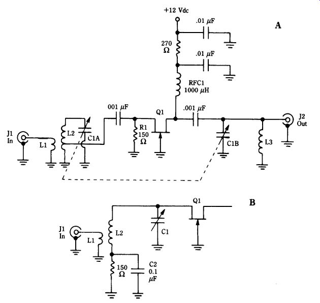
FIG. 3 (A) Grounded-gate JFET preselector circuit and (B) alternate input circuit.
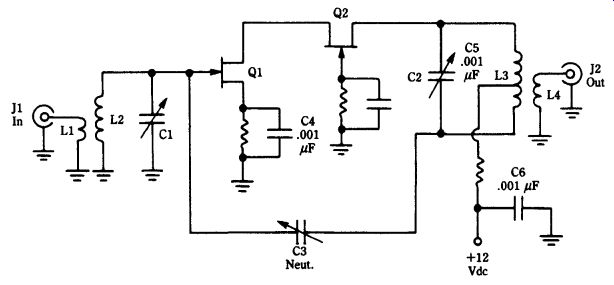
FIG. 4 Cascode active preselector circuit.
The source circuit of the JFET is low-impedance, so some means must be pro vided to match the circuit to the tuned circuit. In Fig. 3A, a tapped inductor is used for L2 (tapped at 1/3 the coil winding); in Fig. 3B, a slightly different configuration is used.
The circuit in Fig. 4 is a VHF preamplifier that uses two JFET devices connected in cascode (i.e., input device Q1 is in common source and is direct coupled to the common gate output device Q2). In order to prevent self-oscillation of the circuit, a neutralization capacitor (NEUT) is provided. This capacitor is adjusted to keep the circuit from oscillating at any frequency within the band of operation. In general, this circuit is tuned to a single channel by the action of L2/C1 and L3/C2.
MOSFET preselector circuits
The 40673 MOSFET used in the following preselector circuit (Fig. 5) is inexpensive and easily available. It is a dual-gate MOSFET. The signal is applied to gate G1, and gate G2 is either biased to a fixed positive voltage or connected to a variable dc voltage that serves as a gain control signal. The dc network is similar to that of the previous (JFET) circuits, with the exception that a resistor voltage divider (R3/R4) is needed to bias gate G2.
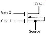
FIG. 5 MOSFET transistor.
There are three tuned circuits for this preselector project, so it will produce a large amount of selectivity improvement and image rejection. The gain of the device will also provide additional sensitivity. All three tuning capacitors (C1A, C16, and C1C) are ganged to the same shaft (Fig. 6) for "single-knob tuning." The trimmer capacitors (C2, C3, and C4) are used to adjust the tracking of the three tuned circuits (i.e., ensure that they are all tuned to the same frequency at any given setting of C1A-C1C).
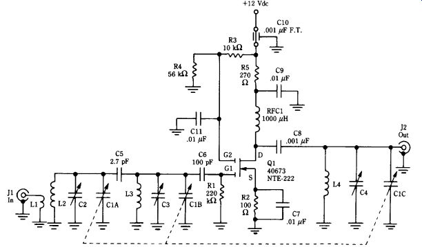
FIG. 6 MOSFET active preselector circuit.
The inductors are of the same sort as described. It is permissible to put L1/L2 and L3 in close proximity to each other, but these should be separated from L4 in order to prevent unwanted oscillation because of feedback arising from coil coupling.
The circuit in Fig. 7 is a little different. In addition to using only input tuning (which lessens the potential for oscillation), it also uses voltage tuning. The hard to-find variable capacitors are replaced with varactor diodes, also called voltage variable-capacitance diodes. These PN junction diodes exhibit a capacitance that is a function of the applied reverse bias potential, VT. Although the original circuit was built and tested for the AM broadcast band (540 to 1610 kHz), it can be changed to any band by correctly selecting the inductor values. The designated varactor (NTE-618) offers a capacitance range of 440 pF down to 15 pF over the voltage range of 0 to _18 Vdc.
The inductors might be either "store-bought" types or wound over toroidal cores. I used a toroid for L1/L2 (forming a fixed inductance for L2) and "store bought" adjustable inductors for L3 and L4. There is no reason, however, why these same inductors cannot be used for all three uses. Unfortunately, not all values are available in the form that has a low-impedance primary winding to permit antenna coupling.
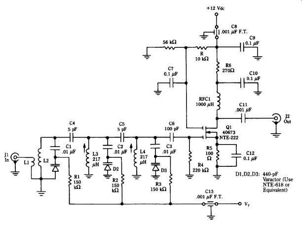
FIG. 7 Varactor-tuned MOSFET active preselector circuit.
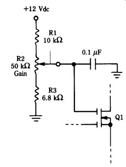
FIG. 8 Variable RF gain control for the MOSFET circuit.
Figure 7 shows the connection points for the dc power (_9 to _12 Vdc).
These points are 0.001-uF ceramic feedthrough capacitors. These are a little hard to find locally, but can be bought from Newark Electronics or other distributors.
In both of the MOSFET circuits, the fixed bias network used to place gate G2 at a positive dc potential can be replaced with a variable voltage circuit, such as Fig. 8. The potentiometer in Fig. 8 can be used as an RF gain control to reduce gain on strong signals and increase it on weak signals. This feature allows the active preselector to be custom set to prevent overloading from strong signals.
Noise and preselectors
The weakest signal that you can detect is determined mainly by the noise level in the receiver. Some noise arrives from outside sources, and other noise is generated inside the receiver. At the VHF/UHF range, the internal noise is predominant, so it is common to use a low-noise preamplifier ahead of the receiver. This preamplifier will reduce the noise figure for the entire receiver. If you select a commercial ready-built or kit VHF preamplifier, such as the units sold by Hamtronics, Inc. ( 65 Moul Rd., Hilton, NY 14468-9535; Phone: 716-392-9430), be sure to specify the low noise variety for the first amplifier in the system.
The low-noise amplifier (LNA) should be mounted on the antenna if it is wide band and at the receiver if it is tunable (notice: the term preselector only applied to tuned versions, while preamplifier could denote either tuned or wideband models).
Of course, if your receiver is used only for one frequency, then it can also be mounted at the antenna. The reason for mounting the antenna right at the antenna is to build up the signal and improve the signal-to-noise ratio (SNR) prior to feeding the signal into the transmission line, where losses cause it to weaken somewhat.
Broadband RF preamplifier for VLF, LF, and AM BCB
In many situations, a broadband (as opposed to tuned) RF amplifier is needed.
Typical applications include boosting the output of RF signal generators (which tend to be normally quite low level), antenna preamplification, loop antenna amplifier, and in the front ends of receivers. A number of different circuits published, including some by me, but one failing that I've noted on most of them is that they often lack response at the low end of the frequency range. Many designs offer -3 dB frequency response limits of 3 to 30 MHz, or 1 to 30 MHz, but rarely are the VLF, LF, or even the entire AM broadcast band (540 to 1700 kHz) covered.
The original need for this amplifier was that I needed an amplifier to boost AM BCB DX signals. Many otherwise fine communications or entertainment-grade "general coverage" receivers operate from 100 kHz to 30 MHz or so, and that range initially sounds really good to the VLF through AM BCB DXer. But when examined closer, it turns out that the receiver lacks sensitivity on the bands below either 2 or 3 MHz, so it fails somewhat in the lower end of the spectrum. Although most listening on the AM BCB is to powerful local stations (where receivers with no RF amplifier and a loop stick antenna will work nicely), those who are interested in DXing are not well served.
In addition to the receiver, I wanted to boost my signal generator 50-ohm output to make it easier to develop some AM and VLF projects that I am working on and to provide a preamplifier for a square-loop antenna that tunes the AM BCB.
Several requirements were developed for the RF amplifier. First, it had to retain the 50-ohm input and output impedances that are standard in RF systems. Second, it had to have a high dynamic range and third-order intercept point in order to cope with the bone-crunching signal levels on the AM BCB. One of the problems of the AM BCB is that those sought after DX stations tend to be buried under multikilowatt local stations on adjacent channels. That's why high dynamic range, high-intercept point loop antennas tend to be required in these applications. I also wanted the amplifier to cover at least two octaves (4:1 frequency ratio), but it achieved a decade (10:1) response (250 to 2500 kHz).
Furthermore, the amplifier circuit had to be easily modifiable to cover other frequency ranges up to 30 MHz. This last requirement would make the amplifier useful to a large number of readers as well as extend its usefulness to me.
Consider a number of issues when designing an RF amplifier for the front end of a receiver. The dynamic range and intercept point requirements were mentioned previously. Another issue is the amount of distortion products (related to third-order intercept point) that are generated in the amplifier. It does no good to have a high capability on the preamplifier only to overload the receiver with a lot of extraneous RF energy it can't handle-energy that was generated by the preamplifier, not from the stations being received. These considerations point to the use of a push-pull RF amplifier design.
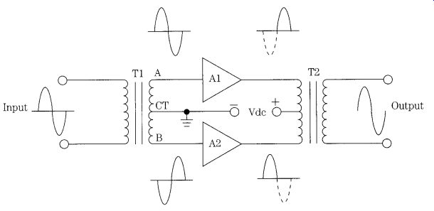
FIG. 9 Push-pull broadband amplifier block diagram.
Push-pull RF amplifiers
The basic concept of a push-pull amplifier is demonstrated in Fig. 9. This type of circuit consists of two identical amplifiers that each process half the input sine wave signal. In the circuit shown, this job is accomplished by using a center-tapped transformer at the input to split the signal and another at the output to recombine the signals from the two transistors. The transformer splits the signal because its center tap is grounded; thus, it serves as the common for the signals applied to the two transistors. Because of normal transformer action, the signal polarity at end "A" will be opposite that at end "B" when the center tap ("CT") is grounded. Thus, the two amplifiers are driven 180 out of phase with each other; one will be turning on while the other is turning off and vice versa.
The push-pull amplifier circuit is balanced, and as a result it has a very interesting property: even-order harmonics are canceled in the output, so the amplifier out put signal will be cleaner than for a single-ended amplifier using the same active amplifier devices.
There are two general categories of push-pull RF amplifiers: tuned amplifiers and wideband amplifiers. The tuned amplifier will have the inductance of the input and output transformers resonated to some specific frequency. In some circuits, the non-tapped winding might be tuned, but in others, a configuration such as Fig. 10 might be used. In this circuit, both halves of the tapped side of the transformer are individually tuned to the desired resonant frequency. Where variable tuning is desired, a split-stator capacitor might be used to supply both capacitances.
The broadband category of circuit is shown in Fig. 11A. In this type of circuit, a special transformer is usually needed. The transformer must be a broadband RF transformer, which means that it must be wound on a suitable core so that the windings are bifilar or trifilar. The particular transformer in Fig. 11A has three windings, of which one is much smaller than the others. These must be trifilar wound for part of the way and bifilar wound the rest of the way. This means that all three windings are kept parallel until no more turns are required of the coupling link. Then, the remaining two windings are kept parallel until they are completed. Figure 7-11B shows an example for the case where the core of the transformer is a ferrite or powdered-iron toroid.
Actual circuit details
The actual RF circuit is shown in Fig. 12; it is derived from a similar circuit found in Doug DeMaw's excellent book W1FB's QRP Notebook (ARRL, 225 Main Street, Newington, CT 06111). The active amplifier devices are JFETs that are intended for service from dc to VHF. The device selected can be the ever-popular MPF-102 or its replacement equivalent from the SK, ECG, or NTE lines of devices.
Also useful is the 2N4416 device. The particular device that I used was the NTE-451 JFET transistor. This device offers a transconductance of 4000 microsiemens, a drain current of 4 to 10 mA, and a power dissipation of 310 mW, with a noise figure of 4 dB maximum.
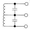
FIG. 10 Tuned-coupling transformer.
The JFET devices are connected to a pair of similar transformers, T1 and T2. The source bias resistor (R1) for the JFETs, and its associated bypass capacitor (C1), are connected to the center tap on the secondary winding of transformer T1. Similarly, the _9-Vdc power-supply voltage is applied through a limiting resistor (R2) to the center tap on the primary of transformer T2.
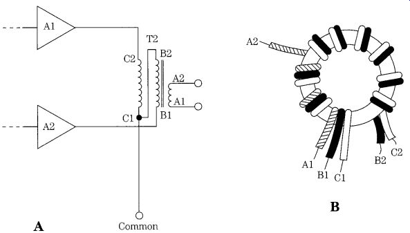
FIG. 11 (A) Untuned (broadband) coupling transformer and (B) winding the transformer
on a toroid.
Take special note of those two transformers. These transformers are known generally as wideband transmission-line transformers and can be wound on either toroid or binocular ferrite or powdered iron cores. For the project at hand, because of the low frequencies involved, I selected a type BN-43-202 binocular core. The type-43 material used in this core is a good selection for the frequency range involved. The core can be obtained from either Amidon Associates or Ocean State Electronics [ P.O. Box 1458, 6 Industrial Drive, Westerly, RI 02891; Phones 401-596-3080 (voice), 401 596-3590 (fax) or 800-866-6626 (orders only)]. Three windings are on each trans former. In each case, the "B" and "C" windings are 12 turns of no. 30 AWG enameled wire wound in a bifilar manner. The coupling link in each is winding "A." The "A" winding on transformer T1 consists of four turns of no. 36 AWG enameled wire, and on T2 it consists of two turns of the same wire. The reason for the difference is that the number of turns in each is determined by the impedance-matching job it must do (T1 has a 1:9 pri /sec ratio, and T2 has a 36:1 pri /sec ratio). Neither the source nor drain impedances of this circuit are 50 _ (the system impedance), so there must be an impedance-transformation function. If the two amplifiers in the circuit were of the sort that had 50-_ input and output impedances, such as the Mini-Circuits MAR-1 through MAR-8 devices, then winding "A" in both transformers would be identical to windings "B" and "C." In that case, the impedance ratio of the transformers would be 1:1:1.
The detail for transformers T1 and T2 is shown in Fig. 13. I elected to build a header of printed circuit perforated board for this part; the board holes are on 0.100 in centers. The PC type of perfboard has a square or circular printed circuit soldering pad at each hole. A section of perfboard was cut with a matrix of 5 _ 9 holes. Vector Electronics push terminals are inserted from the unprinted side then soldered into place. These terminals serve as anchors for the wires that will form the windings of the transformer. Two terminals are placed at one end of the header, and three are placed at the opposite end.
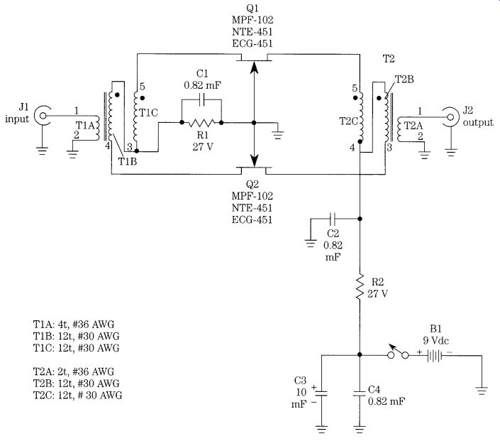
FIG. 12 JFET push-pull broadband amplifier.
The coupling winding is connected to pins 1 and 2 of the header and is wound first on each transformer. Strip the insulation from a length of no. 36 AWG enameled wire for about 1/4 from one end. This can be done by scraping with a scalpel or X-acto knife or by burning with the tip of a soldering pencil. Ensure that the exposed end is tinned with solder then wrap it around terminal 1 of the header. Pass the wire through the first hole of the binocular core, across the barrier between the two holes, and then through the second hole. This U-shaped turn counts as one turn. To make transformer T1 pass the wire through both sets of holes three more times (to make four turns). The wire should be back at the same end of the header as it started. Cut the wire to allow a short length to connect to pin 2. Clean the insulation off this free end, tin the exposed portion, then wrap it around pin 2 and solder. The primary of T1 is now completed.
FIG. 13 Winding the coupling transformers using a bazooka core and a perfboard
or printed circuit header.
The two secondary windings are wound together in the bifilar manner and consist of 12 turns each of no. 30 AWG enameled wire. The best approach seems to be twisting the two wires together. I use an electric drill to accomplish this job.
Two pieces of wire, each 30 long, are joined together and chucked up in an electric drill. The other ends of the wire are joined together and anchored in a bench vise or some other holding mechanism. I then back off and hold the drill in one hand, until the wire is nearly taut. Turning on the drill causes the two wires to twist together. Keep twisting them until you obtain a pitch of about 8 to 12 twists per inch.
It is very important to use a drill that has a variable speed control so that the drill chuck can be made to turn very slowly. It is also very important that you follow certain safety rules-especially with regard to your eyesight, when making twisted pairs of wire. Be absolutely sure to wear either safety glasses or goggles while doing this operation. If the wire breaks, and that is a common problem, then it will whip around as the drill chuck turns. Although no. 36 wire doesn't seem to be very substantial, at high speed it can severely injure an eye.
To start the secondary windings, scrap all of the insulation off both wires at one end of the twisted pair and tin the exposed ends with solder. Solder one of these wires to pin 3 of the header and the other to pin 4. Pass the wire through the hole of the core closest to pin 3, around the barrier, then through the second hole, returning to the same end of the header where you started. That constitutes one turn. Now do it 11 more times until all 12 turns are wound. When the 12 turns are completed, cut the twisted pair wires off to leave about 1/2 free. Scrape and tin the ends of these wires.
Connecting the free ends of the twisted wire is easy, but you will need an ohmmeter or continuity tester to see which wire goes where. Identify the end that is connected at its other end to pin 3 of the header and connect this wire to pin 4. The remaining wire should be the one that was connected at its other end to pin 4 earlier; this wire should be connected to pin 5 of the header.
Transformer T2 is made in the identical manner as transformer T1, but with only two turns on the coupling winding, rather than four. In this case, the coupling winding is the secondary, and the other two form two halves of the primary. Wind the two turn secondary first, as was done with the four-turn primary on T1.
The amplifier can be built on the same sort of perforated board as was used to make the headers for the transformers. Indeed, the headers and the board can be cut from the same stock. The size of the board will depend somewhat on the exact box you select to mount it in. For my purposes, the box was a Hammond 3 _ 5.5 _ 1.5 cabinet. Allowing room for the 9-Vdc battery at one end, and the input/output jacks and power switch at the other, left me with 2.5 _ 3.5 of available space in which to build the circuit (Fig. 14). For those who wish to experiment with a printed circuit board.
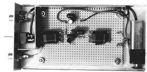
FIG. 14 Completed preamplifier.
I built the circuit from the output end backward toward the input, so trans former T2 was mounted first with pins 1 and 2 toward the end of the perfboard. Next, the two JFET devices were mounted, and then T1 was soldered into place. After that, the two resistors and capacitors were added to the circuit. Connecting the elements together and providing push terminals for the input, output, dc power supply ground, and the _9 Vdc finished the board.
Because the input and output jacks are so close together, and because the dc power wire from the battery to the switch had to run the length of the box, I decided to use a shield partition to keep the input and output separated. This partition was made from 1-in brass stock. This material can be purchased at almost any hobby shop that caters to model builders. The RG-174/U coaxial cable between the input jack on the front panel and the input terminals on the perfboard run on the outside of the shield partition.
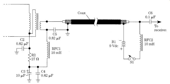
FIG. 15 Powering a remote preamplifier.
Variations on the theme
Three variations on the circuit extend the usefulness for many different readers.
First, there are those who want to use the amplifier at the output of a loop antenna that is remote mounted. It isn't easy to go up to the roof or attic to turn on the amplifier any time you wish to use the loop antenna. Therefore, it is better to install the 9-Vdc power source at the receiver end and pass the dc power up the coaxial cable to the amplifier and antenna. This method is shown in Fig. 15. At the receiver end, RF is isolated from the dc power source by a 10-mH RF choke (RFC2), and the dc is kept from affecting the receiver input (which could short it to ground!) by using a blocking capacitor (C4). All of these components should be mounted inside of a shielded box. At the amplifier end, lift the grounded side of the T2 secondary and connect it to RFC2, which is then connected to the _9-Vdc terminal on the perfboard. A decoupling capacitor (C3) keeps the "cold" end of the T2 secondary at ground potential for RF, while keeping it isolated from ground for dc.
A second variation is to build the amplifier for shortwave bands. This can be accomplished easily enough. First, reduce all capacitors to 0.1 uF. Second, build the transformers (T1 and T2) on a toroid core rather than the binocular core. In the original design (op. cit.), a type TF-37-43 ferrite core was used with the same 12:12:2 and 12:12:4 turns scheme as used.
Alternatively, select a powdered-iron core, such as T-50-2 (RED) or T-50-6 (YEL). I suspect that about 20 turns will be needed for the large windings, 4 turns for the "A" winding on T2, and 7 turns for the "A" winding on T1. You can experiment with various cores and turns counts to optimize for the specific section of the short wave spectrum that you wish to cover.
The third variation is to make the amplifier operate on a much lower frequency (e.g., well down into the VLF region). The principal changes needed are in the cores used for transformers T1 and T2, the number of turns of wire needed, and the capacitors needed. The type 43 core will work down to 10 kHz or so but requires a lot more turns to work efficiently in that region. The type 73 material, which is found in the BN-73-202 core, will provide an AL value of 8500 as opposed to 2890 for the BN-43 202 device used in this section. Doubling the number of turns in each winding is a good starting point for amplifiers below 200 kHz. The type 73 core works down to 1 kHz, so with a reasonable number of turns should work in the 20- to 100-Hz range as well.
Broadband RF amplifier (50-ohm input and output)
This project is a highly useful RF amplifier that can be used in a variety of ways.
It can be used as a preamplifier for receivers operating in the 3- to 30-MHz shortwave band. It can also be used as a postamplifier following filters, mixers, and other de vices that have an attenuation factor. It is common, for example, to find that mixers and crystal filters have a signal loss of 5 to 8 dB (this is called insertion loss). An amplifier following these devices will overcome that loss. The amplifier can also be used to boost the output level of signal generator and oscillator circuits. In this ser vice, it can be used either alone, in its own shielded container, or as part of another circuit containing an oscillator circuit.
The circuit is shown in Fig. 16A. This circuit was originated by Hayward and used extensively by Doug DeMaw in various projects. The transistor (Q1) is a 2N5179 broadband RF transistor. It can be replaced by the NTE-316 or ECG-316 devices, if the original is not available to you. The NTE and ECG devices are intended for service and maintenance replacement applications, so they are often sold by the local electronic parts distributors.
This amplifier has two important characteristics: the degenerative feedback in the emitter circuit and the feedback from collector to base. Degenerative, or negative, feedback is used in amplifiers to reduce distortion (i.e., make it more linear) and to stabilize the amplifier. One of the negative feedback mechanisms of this amplifier is seen in the emitter. The emitter resistance consists of two resistors, R5 is 10 ohm and R6 is 100 ohm. In most amplifier circuits, the emitter resistor is bypassed by a capacitor to set the emitter of the transistor at ground potential for RF signals, while keeping it at the dc level set by the resistance. In normal situations, the reactance of the capacitor should be not more than one-tenth the resistance of the emitter resistor. The 10-ohm portion of the total resistance is left unbypassed, forming a small amount of negative feedback.
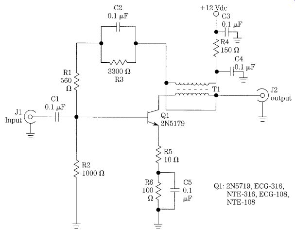
FIG. 16 Feedback NPN transistor preamplifier.
The collector to base feedback is accomplished by two means. First, a resistor capacitor network (R1/R3/C2) is used; second, a 1:1 broadband RF transformer (T1) is used. This transformer can be homemade. Wind 15 bifilar turns of no. 26 enameled wire on a toroidal core, such as the T-50-2 (RED) or T-50-6 (YEL); smaller cores can also be used.
The circuit can be built on perforated wireboard that has a grid of holes on 0.100-in centers. Alternatively, you can use the printed circuit board pattern shown in Fig. 16B. In this version of the project, the PC board is designed for use with a Mini-Circuits 1:1 broadband RF transformer. Alternatively, use a homebrew trans former made on a small toroidal core. Use the size 37 core, with no. 36 enameled wire. As in the previous case, make the two windings bifilar.
Broadband or tuned RF/IF amplifier using the MC-1350P
The MC-1350P is a variant of the MC-1590 device, but unlike the 1590, it is avail able in the popular and easy-to-use eight-pin mini-DIP package. It has gain sufficient to make a 30-dB amplifier, although it is a bit finicky and tends to oscillate if the circuit is not built correctly. Layout, in other words, can be a very critical factor because of the gain.
If you cannot find the MC-1350P, use the NTE-746 or ECG-746. These devices are MC-1350Ps, but are sold in the service and maintenance replacement lines and are usually available locally.
Figure 17A shows the basic circuit for the MC-1350P amplifier. The signal is applied to the _IN input, pin 4, and the _IN input is decoupled to ground with a 0.1-uF capacitor. All capacitors in this circuit, except C6 and C7, should be disk ceramic or one of the newer dielectrics that are competent at RF frequencies to 30 MHz. A capacitor in series with the input terminal, C1, is used to prevent dc riding on the signal from affecting the internal circuitry of the MC-1350P.
The output circuitry is connected to pin 1 of the MC-1350P. Because this circuit is broadband, the output impedance load is an RF choke (L1). For most HF application, L1 can be a 1-mH choke, although for the lower end of the shortwave region and the AM broadcast band, use a 2.5-mH choke. The same circuit can be used for 455-kHz IF amplifier service if the coil (L1) is made 10 mH.
Pin 5 of the MC-1350P device is used for gain control. This terminal needs to see a voltage of +5 to +9 V, with the maximum gain at the +5-V end of the range (this is opposite what is seen in other chips). The gain-control pin is bypassed for RF signals.
The dc power supply is connected to pins 8 and 2 simultaneously. These pins are decoupled to ground for RF by capacitor C4. The ground for both signals and dc power are at pins 3 and 7. The V_ is isolated somewhat by a 100-ohm resistor (R3) in series with the dc power-supply line. The V_ line is decoupled on either side of this resistor by electrolytic capacitors. C6 should be a 4.7- to 10-uF tantalum capacitor, and C7 is a 68-uF (or greater) tantalum or aluminum electrolytic capacitor.
A partial circuit with an alternate output circuit is shown in Fig. 17B. This circuit is tuned, rather than broadband, so it could be used for IF amplification or RF amplification at specific frequencies. Capacitor C8 is connected in parallel with the inductance of L1, tuning L1 to a specific frequency. In order to keep the circuit from oscillating the resonant tank circuit is "de-Q-ed" by connecting a 2.2-k_ resistor in parallel with the tank circuit. Although considered optional in Fig. 17A, it is not optional in this circuit if you want to prevent oscillation.
Figure 17C shows a printed circuit board pattern that can be used for building the circuit of Fig. 17A. The spacing of the holes for the inductor are de signed to accommodate the Toko line of fixed inductors from Digi-Key (use sizes 7 or 10).
The MC-1350P device has a disgusting tendency to oscillate at higher gains. One perfboard version of the Fig. 17A circuit that I built would not produce more than 16 dB without breaking into oscillation. One tactic to prevent the oscillation is to use a shield between the input and output of the MC-1350P. Extra holes are on the printed circuit pattern to anchor a shield. The shield should be made of copper or brass stock sheet metal, such as the type that can be bought at hobby shops. Cut a small notch along one edge of a piece of 1 stock. The notch should be just large enough to fit over the MC-1350P without shorting out. The location of the shield is shown by the dotted line in Fig. 17A. Notice that it is bent a little bit in order to fit from the two ground pins on the MC-1350P (i.e., pins 2 and 7).
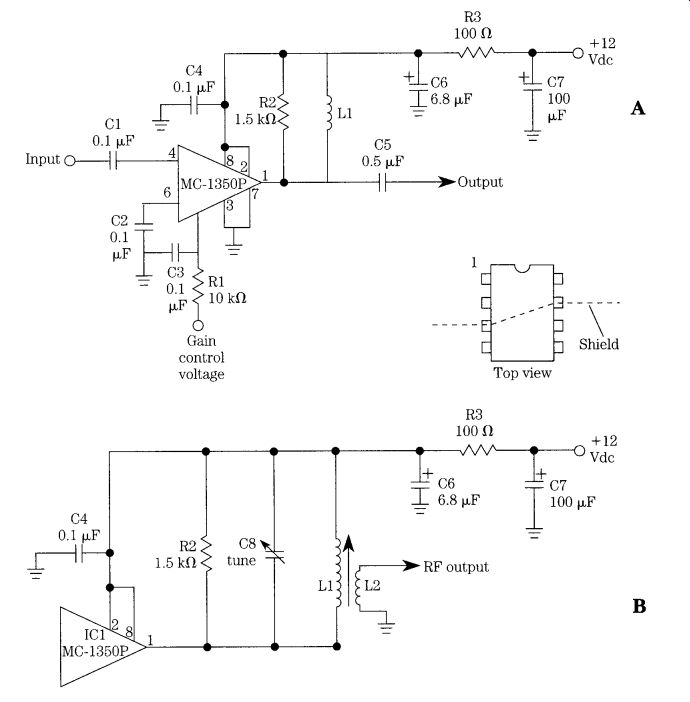
FIG. 17 (A) MC-1350P preamplifier; (B) alternate output circuit; and (C) printed
circuit board pattern.
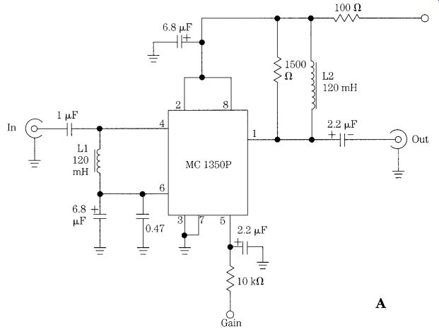
FIG. 18 (A) Circuit for a MC-1350P preamplifier (alternate version) and (B)
printed circuit pat tern.
VLF preamplifier
The VLF bands run from 5 or 10 to 500 kHz or just about everything below the AM broadcast band. The frequencies above about 300 kHz can be accommodated by circuitry not unlike 455-kHz IF amplifiers. But as frequency decreases, it becomes more of a problem to build a good preamplifier. This project is a preamplifier designed for use from 5 to 100 kHz. This band contains a lot of Navy communications, as well as the most accurate time and frequency station, operated by the National Institute of Science and Technology (NIST), WWVB. The operating frequency of WWVB is a very accurate 60 kHz and is used as a frequency standard in many situations. The signal of WWVB is also used to update electronic clocks.
The circuit of Fig. 18A is similar to Fig. 17A, except that a large-value RF choke (L1) is used across the _IN and _IN terminals. Both of these chokes are 120 mH 10 Toko units. If oscillation occurs, then select a different value (82 or 100 mH) for one of these chokes. The problem is that the chokes have a capacitance between windings and that capacitance can resonate the choke to a frequency (this is the "self-resonance" factor). By using different values of chokes in the input and output circuits, their self-resonant frequencies are moved away from each other, reducing the chance of oscillation.
Conclusion
A preselector can improve the performance of your receiver, no matter whether you listen to VLF, AM broadcast band, shortwave, or VHF/UHF bands. The circuits presented in this section allow you to "roll your own" and be successful at it.