AMAZON multi-meters discounts AMAZON oscilloscope discounts
Most of the gain and selectivity of a superheterodyne radio receiver are in the intermediate frequency (IF) amplifier. The IF amplifier is, therefore, a high-gain, narrow bandwidth amplifier. Typically, IF power gains run in the 60- to 120-dB range, depending on the receiver design. It usually has far narrower bandwidth than the RF amplifier. For example, 2.8 KHz for an SSB receiver and 500 Hz for a CW receiver.
The purpose of the IF amplifier is to provide gain and selectivity to the receiver.
The selectivity portion of the equation is provided by any of several different types of filter circuit. FIG. 1 shows several different filters used in IF amplifiers. The classical circuit is shown in Fig. 1A. This transformer is shown with taps, but it may also exist without the taps. The taps provide a low-impedance connection while retaining the overall advantages of high-impedance tuned circuits. Note that the capacitors are usually inside the transformer shielded can. A slightly different version is shown in Fig. 1B. This transformer differs from the one previous in that the secondary winding is capacitor coupled to its load and that capacitor may or may not be resonating. Still a third version is had by making the secondary winding an untuned low-impedance loop.
A somewhat different approach is shown in Fig. 1C. This transformer is a series-resonant tapped circuit on the input end and parallel-tuned and tapped on the output end. It requires two shield cans to implement this approach.
Finally, we have the representation shown in Fig. 1D. This symbol represents any of several mechanical or crystal filters. Such filters usually give a much narrower bandwidth than the LC filters discussed previously.
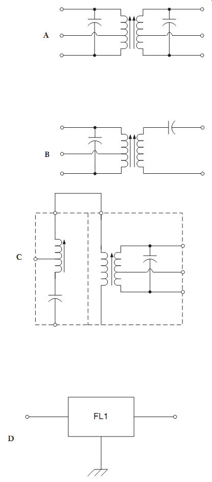
FIG. 1 Various IF filters.
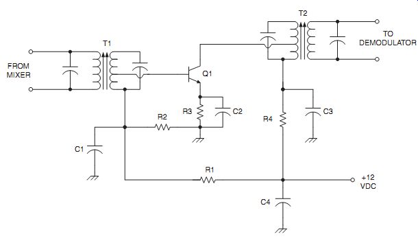
FIG. 2 Simple transistor IF amplifier.
Amplifier circuits
A simple IF amplifier is shown in Fig. 2. A simple AM band radio may have one such stage, while FM receivers, shortwave receivers, and other types of communications receiver may have two to four stages such as Fig. 2. This IF amplifier is based on the type of LC filter circuits discussed in Fig. 1A. Transformer T1 has a low impedance tap on its secondary connected to the base of a transistor (Q1). Similarly with T2, but in this case the primary winding is tapped for the collector of the transistor. The bias for the transistor is provided by resistors R1 and R2, with capacitor C1 being used to place the cold end of the T1 secondary at ground potential for ac signals. Resistor R3 is used to provide a bit of stability to the circuit. Capacitor C2 is used to keep the emitter of the transistor at ground potential for ac signals, while keeping it at a potential of IER3 for dc. The reactance of capacitor C2 should be _R3/10. Resistor R4 forms part of the collector load for transistor Q1. Capacitors C3 and C4 are used to bypass and decouple the circuit.
FIG. 3 shows a gain-controlled version of Fig. 2. This particular circuit is designed for a low frequency (240 to 500 KHz), although with certain component value changes it could be used for higher frequencies as well. Another difference be tween this circuit and the circuit of Fig. 2 is that this circuit has double-tapped transformers for T1 and T2.
The major change is the provision for automatic gain control. A capacitor is used to sample the signal for some sort of AGC circuit. Furthermore, the circuit has an additional resistor (R3) to the dc control voltage of the AGC circuit.
Cascode pair amplifier
A cascode pair amplifier is shown in Fig. 4. This amplifier uses two transistors (both JFETs) in an arrangement that puts Q1 in the common source configuration and Q2 in the common gate configuration. The two transistors are direct-coupled. In put and output tuning is accomplished by a pair of LC filters (L2C1 and L3C2). To keep this circuit from oscillating at the IF frequency a neutralization capacitor (C3) is provided. This capacitor is connected from the output LC filter on Q2 to the input of Q1.
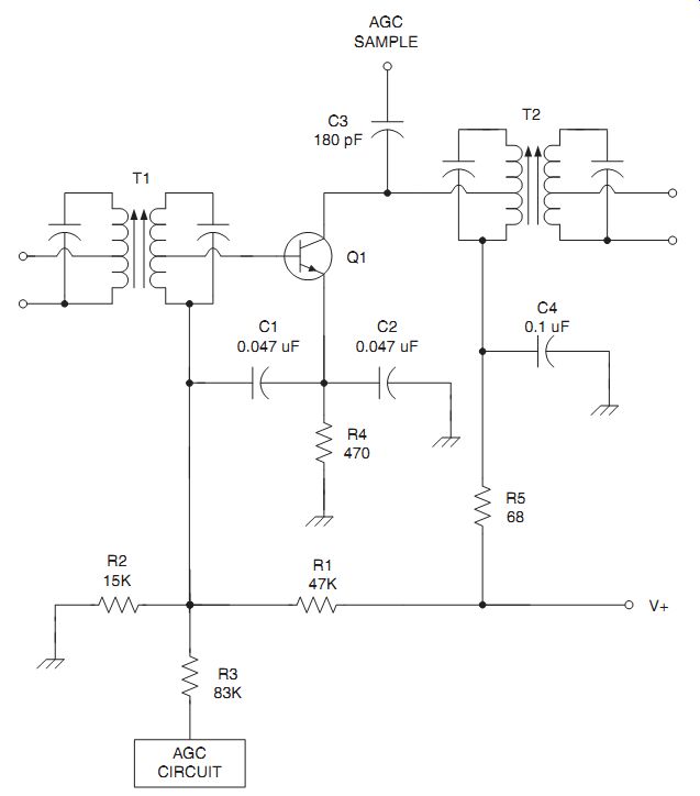
FIG. 3 Simple IF amplifier with AGC.
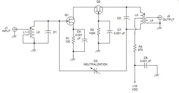
FIG. 4 Cascode JFET IF amplifier.
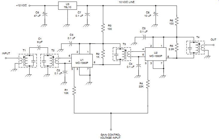
FIG. 5 IF amplifier with crystal filter.
"Universal" IF amplifier
The IF amplifier in Fig. 5 is based on the popular MC-1350P integrated circuit.
This chip is easily available through any of the major mail order parts houses and many small ones. It is basically a variation on the LM-1490 and LM-1590 type of circuit but is a little easier to apply.
If you have difficulty locating MC-1350P devices, the exact same chip is available in the service replacement lines such as ECG and NTE. These parts lines are sold at local electronics parts distributors and are intended for the service repair shop trade. I used actual MC-1350P chips in one version and NTE-746 (same as ECG-746) chips in the other without any difference in performance. The NTE and ECG chips are actually purchased from the sources of the original devices and then re-numbered.
The circuit is shown in Fig. 5. Two MC-1350P devices in cascade are used.
Each device has a differential input (pins 4 and 6). These pins are connected to the link windings on IF transformers (e.g., T2 at device U1 and T3 at U2). In both cases, one of the input pins are grounded for AC (i.e., RF and IF) signals through a bypass capacitor (C2 and C4).
In the past I've had difficulties applying the MC-1350P devices when two were used in cascade. The problem is that these are high-gain chips and any coupling at all will cause oscillation. I've built several really good MC-1350P oscillators-the problem is that I was building IF amplifiers. The problem is basically solved by two tactics that I'd ignored in the past. This time I reversed the connections to the input terminals on the two devices. Note that pin 4 is bypassed to ground on U1, while on U2 it is pin 6. The other tactic is to use different value resistors at pin 5.
Pin 5 on the MC-1350P device is the gain control pin. It is used to provide either manual gain control (MGC) or automatic gain control (AGC). The voltage applied to this pin should be between _3 and _9 V, with the highest gain being at _3 V and nearly zero gain at _9 V.
The outputs of the MC-1350P are connected to the primaries of T3 and T4. Each output circuit has a resistor (R2 and R5) across the transformer winding. The transformers used are standard "transistor radio" IF transformers provided that the impedance matching requirements are met.
The DC power is applied to the MC-1350P devices through pins 1 and 2, which are connected together. Bypass capacitors C3 and C5 are used to decouple the DC power lines and thereby prevent oscillation. All of the bypass capacitors (C2, C3, C4, and C5) should be mounted as close to the bodies of U1 and U2 as possible. They can be disk ceramic devices, or some of the newer dielectric capacitors, provided of course that they are rated for operation at the frequency you select. Most capacitors will work to 10.7 MHz, but if you go to 50 MHz or so, some capacitor types might show too much reactance (disk ceramic devices work fine at those frequencies, how ever).
The dc power supply should be regulated at some voltage between _9 and _15 Vdc. More gain can be obtained at _15 Vdc, but I used _10 Vdc with good results.
In each power line there is a 100-ohm resistor (R3 and R6), which help provide some isolation between the two devices. Feedback via the power line is one source of oscillation in high-frequency circuits.
The dc power line is decoupled by two capacitors. C7 is a 0.1-uF capacitor and is used to decouple high frequencies that either get in through the regulator or try to couple from chip to chip via the dc power line (which is why they are called "decoupling" capacitors). The other capacitor (C8) is a 10- to 100-uF device used to smooth out any variations in the dc power or to decouple low frequencies that the 0.1 uF doesn't take out effectively.
The RF/IF input circuit deserves some comment. I elected to use a double-tuned arrangement. This type of circuit is of a category that are coupled via a mutual reactance. Various versions of this type of circuit are known, but I elected to use the version that uses a capacitive reactance (C1) at the "hot" end of the LC tank circuits.
Coupling in and out of the network is provided by the transformer coupling links.
The power and gain control connections are bought through the aluminum box wall through 1000-pF feedthrough capacitors. Two kinds are available, one solder-in and the other screw thread-mounted. For aluminum boxes the screw thread is needed because it is difficult to solder to aluminum. Both types are available in either 1000- or 2000-pF values, either of which can be used in this application. If you elect to use some other form of connector, then add disk ceramic capacitors (0.001 uF) to the connector, right across the pins as close as possible to the connector.
There are several ways to make this circuit work at other frequencies. If you want to use a standard IF frequency up to 45 MHz or so, then select one with the configuration shown in Fig. 5 (these are standard). If you want to make the circuit operate in the HF band on a frequency other than 10.7 MHz, then it's possible to use the 10.7-MHz transformer. If the desired frequency is less than 10.7 MHz, then add a small value fixed or trimmer capacitor in parallel with the tuned winding. It will add to the built-in capacitance, reducing the resonant frequency. I don't know how low you can go, but I've had good results at the 40-m amateur band (7-7.3 MHz) using additional capacitance across a 10.7-MHz IF transformer.
On frequencies higher than 10.7 MHz you must take some more drastic action.
Take one of the transformers and turn it over so that you can see the pins. In the middle of the bottom header, between the two rows of pins, there will be an indentation containing the tuning capacitor. It is a small tubular ceramic capacitor (you may need a magnifying glass to see it well if your eyes are like mine). If it is color coded you can obtain the value using your knowledge of the standard color code.
Take a small screwdriver and crush the capacitor. Clean out all of the debris to pre vent shorts at a later time. You now have an untuned transformer with an inductance right around 2 uH. Using this information, you can calculate the required capacitance using this formula:
(Eqn. 1)
…where…
C is the capacitance in picofarads
f is the desired frequency in kilohertz (kHz)
LuH is the inductance in microhenrys.
Equation (Eqn. 1) is based on the standard L-C resonance equation, solved for C, and with all constants and conversion factors rolled into the numerator. If you know the capacitance that must be used, and need to calculate the inductance, then swap the L and C terms in Eq. (Eqn. 1).
If the original capacitor was marked as to value or color-coded, then you can calculate the approximate capacitance needed by taking the ratio of the old frequency to the new frequency and not replacing them with some other capacitor. In that case, IF filtering is done at the input (between the IF amplifier and the mixer circuit).
If the original capacitor was marked as to value or color-coded, then you can calculate the approximate capacitance needed by taking the ratio of the old frequency to the new frequency and then square it. The square of the frequency ratio is the capacitance ratio, so multiply the old capacitance by the square of the frequency ratio to find the new value. For example, suppose a 110-pF capacitor is used for 10.7 MHz, and you want to make a 20.5-MHz coil. The ratio is (10.7/20.5)2 _ 0.272 MHz. The new capacitance will be about 0.272 _ 110 pF _ 30 pF. For other frequencies, you might consider using homebrew toroid inductors.
A variation on the theme is to make the circuit wideband. This can be done for a wide portion of the HF spectrum by removing the capacitors from the transformers and not replacing them with some other capacitor. In that case, IF filtering is done at the input (between the IF amplifier and the mixer circuit).
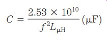
Coupling to other filters
Crystal and mechanical filters require certain coupling methods. FIG. 6 shows a method for coupling to a crystal filter connected between two bipolar transistors. Each stage of the amplifier is a common emitter bipolar transistor amplifier, biased by R1/R2 and R5/R6. The connection to the filter circuit is direct because the filter is not sensitive to dc (such cannot be said of mechanical filters).
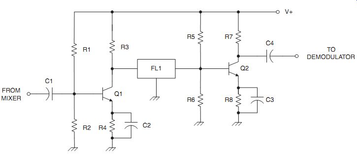
FIG. 6 Universal IF amplifier.
FIG. 7 shows a different approach that accommodates mechanical filters as well as crystal filters. The particular circuit shown is for very high frequency IF amplifiers (e.g., 50 MHz), but with changes to the values of the components, this IF amplifier could be used from VLF through VHF regions. The resonant frequency of this circuit is set by L1 and C1 and the filter circuit. The amplifier is a MOSFET transistor device connected in the common source configuration. Gate G1 is used for the signal and G2 is used for DC bias and gain control (see "AGC").
The filter is connected to the filter through a capacitor to block the dc at the drain of the MOSFET device (similar capacitors would be used in bipolar circuits as well). The output of the filter may or may not be capacitor coupled depending upon the design of the circuits to follow this one.
FIG. 7 MOSFET IF amplifier with AGC.
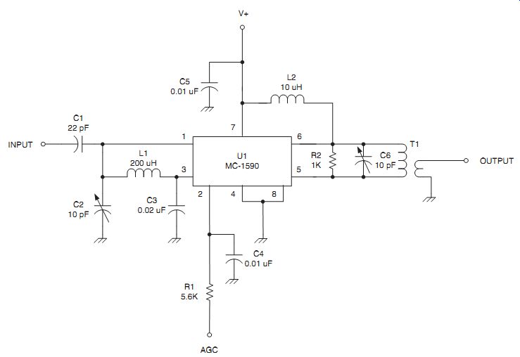
FIG. 8 MC-1590 IF amplifier.
IC IF amplifiers
The universal IF amplifier presented earlier is an example of an integrated circuit (IC) IF amplifier. In this section we will take a look at several additional IC IF amplifier circuits.
MC-1590 circuit
FIG. 8 shows an amplifier based on the 1490 or 1590 chips. This particular circuit works well in the VHF region (30 to 80 MHz). Input signal is coupled to the IC through capacitor C1. Tuning is accomplished by C2 and L1, which forms a parallel resonant tank circuit. Capacitor C3 sets the unused differential input of the 1590 chip to ground potential, while retaining its dc level.
Output tuning in Fig. 8 reflects the fact that the 1590 chip is differential out put as well as differential input. The LC-tuned circuit, consisting of the primary of T1 and capacitor C6, is parallel-resonant and is connected between pins 5 and 6. A resistor across the tank circuit reduces its loaded Q, which has the effect of broadening the response of the circuit.
V_ power is applied to the chip both through the V_ terminal and pin 6 through the coil L2. Pin 2 is used as an AGC gain-control terminal.
SL560C circuits
The SL560C is basically a gain block that can be used at RF and IF frequencies.
FIG. 9 shows a circuit based on the SL560C. The input of the SL560C is differential, but this is a single-ended circuit. That requires the unused input to be by passed to ground through capacitor C3. Because this is a wideband circuit, there is no tuning associated with the input or output circuitry. The input circuitry consists of a 0.02-uF coupling capacitor and an RF choke (RFC1).
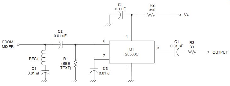
FIG. 9 SL-560C IF amplifier.
A tuned circuit version of the circuit is shown in Fig. 10. This circuit replaces the input circuitry with a tuned circuit (T1) and places a transformer (T2) in the out put circuit. Also different is that the V_ circuit in this case uses a zener diode to regulate the dc voltage.
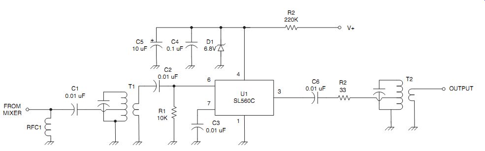
FIG. 10 SL560C IF amplifier (tuned circuit version).
IF processing ICs
There are several forms of IC used for IF processing. The CA3189E (Fig. 11) is one of several that are used in broadcast and communications receivers. The input circuitry consists of a filter, although LC-tuned circuits could be used as well. In this version, the filter circuit is coupled via a pair of capacitors (C1 and C2) to the CA3189E. The input impedance is set by resistor R1 and should reflect the needs of the filter rather than the IC (filters don't produce the same response when mis matched).
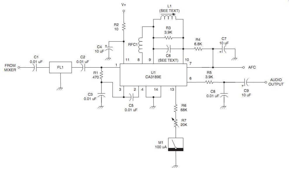
FIG. 11 CA3189E FM IF system.
The CA3189E is an IF gain block and demodulator circuit, all in one IC. Coil L1 and C6 are used for the quadrature detector and their value depends on the frequency used. There are three outputs used on the CA3189E. The audio output is de rived from the demodulator, as is the automatic frequency control (AFC) output.
There is also a signal-strength output that can be used to drive an S-meter (M1) or left blank.
Successive detection logarithmic amplifiers
Where signal level information is required, or where instantaneous outputs are required over a wide range of input signal levels, a logarithmic amplifier might be used. Linear amplifiers have a gain limit of about 100 dB, but only have head room of 3 to 6 dB in some circumstances. One solution to the problem is the logarithmic amplifier. Radar receivers frequently use log amps in the IF amplifier stages.
The successive detection method is used because it is difficult to produce high gain logarithmic amplifiers. The successive detection method uses several log amps and then detects all outputs and sums these outputs together. Each amplifier has an output voltage equal to:
Vo _ k log Vin, (Eqn. 2) where
Vo is the output voltage
Vin is the input voltage
k is a constant.
The circuit shown in Fig. 12A is such an amplifier, while Fig. 12B shows a hypothetical output-vs-input characteristic for the amplifier. Because the circuit uses four or more stages of nonlinear amplification, signals are amplitude-compressed in this amplifier. Because of this, the amplifier is sometimes called a compression amplifier.
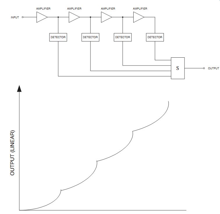
FIG. 12 Output of compression amplifiers.
Filter switching in IF amplifiers
Switching filters is necessary to accommodate different modes of transmission.
AM requires 4 or 6 KHz on shortwave and 8 KHz on the AM broadcast band (BCB).
Single-sideband requires 2.8 KHz, RTTY/RATT requires 1.8 KHz, and CW requires either 270 or 500 Hz. Similarly, FM might require 150 KHz for the FM BCB and as little as 5 KHz on land-mobile communications equipment. These various modes of transmission require different filters, and those filters have to be switched in and out of the circuit.
The switching could be done directly, but that requires either a coaxial cable between the switch and the filter or placing the switch at the site of the filters. A better solution is found in Fig. 13: diode switching. A diode has the unique ability to pass a small ac signal on top of the dc bias. In Fig. 13 switch S1 is used to apply the proper polarity voltage to the diodes in the circuit. In one sense of S1, the positive voltage is applied to D4 through the primary winding of T2, through RFC4 and RFC2, to D3 and then through the secondary winding of T1 to ground. This same current flow reverse biases diodes D1 and D2. The response is to turn on filter FL2. Similarly when S1 is turned to the other position. In that case D1 and D2 are forward biased, selecting FL1, and D3-D4 are reverse biased.
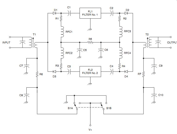
FIG. 13 Dual filter scheme.