AMAZON multi-meters discounts AMAZON oscilloscope discounts
Although the transistor amplifiers we looked at in Section 10 are useful for all sorts of applications, designers of amplifier systems are turning more and more to integrated circuit designs. The operational amplifier (the name goes back to the days when analog computers were more widely used, but that's another story ... ) is perhaps the basic building-block of linear electronic systems. The 'op-amp' (a commonly used abbreviation) is designed to be a close approximation to a perfect amplifier. Here is a specification for such a perfect device:
1. Gain. This should be infinitely high. Obviously an amplifier with infinite gain would be useless, as the smallest input would result in full output! As we shall see, a very high or even infinite gain can be controlled by suitable feedback.
2. Input resistance. Ideally, this should also be infinite, so that there is no loading of the input source at all.
3. Output resistance. Ideally, this should be zero. With a zero output resistance, the amplifier can be connected to a load of any resistance without the output voltage being affected.
4. Bandwidth. This should be infinite, which means that the amplifier should be able to amplify (infinitely!) any frequency from zero (direct voltage) to light!
5. Common mode rejection ratio. This, too, should be infinite, but an explanation is needed. An operational amplifier has one output, but two inputs, an inverting input and a non-inverting input. Fig. 1 shows an op-amp system, with the two inputs clearly marked,'-' for inverting and '+' for non-inverting. A positive voltage applied to the inverting input makes the output swing negative and a positive voltage applied to the non-inverting input makes the output swing positive. It is vital to note that the inputs are relative to each other and not to either of the supply lines. Thus, if both inputs (common mode) are made more positive or negative, there should be no output. This is illustrated in Fig. 2.
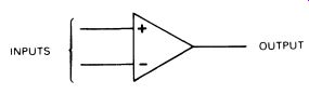
FIG. 1 circuit symbol for an operational amplifier
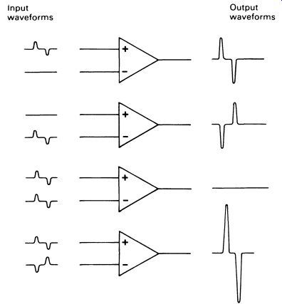
Fig. 2 showing
the output of the op-amp for various types of input
6. Supply voltage. The amplifier should be unaffected by reasonable variations in its power supply voltage.
Now we can compare the theoretical specifications with a real one-the specification for the SN72741 op-amp:
1. Gain: 200 000 voltage gain, about 106 dB.
2. Output resistance: 75 ohm.
3 . Input resistance: 2 M-ohm.
4. Bandwidth: d.c. to 1 MHz.
5. Common mode rejection ratio: 90 dB (i.e. a signal applied to both inputs will be at least 32 000 times smaller than the same signal applied to one input).
6. Supply voltage: output will change less than 150 uV per volt change in the power supply.
The amplifier will operate from a supply of + and -3 to 18 V (see below) and takes a quiescent supply current of about 2mA. The maximum power dissipation is 50mW, and the maximum output current is around 30 mA, by no means perfect, but not bad for a device retailing at less than the price of a cup of coffee! The SN72741 is far from being a 'state of the art' device, but it is a good general purpose op-amp, ideal for all sorts of commercial (i.e. cost-effective) designs, and very suitable for demonstrations and experiments.
Fig. 3 shows the connections to this integrated circuit, which is most commonly available in an 8-pin DIL pack.
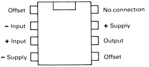
FIG. 3 the SN72741 op-amp integrated circuit
Offset No connection
-Input +Supply
+Input Output
-Supply Offset
The pins marked 'offset' can for the most part be ignored. They are there to compensate for a small design problem with the SN72741, namely the fact that with both inputs at exactly the same potential the output may be a fraction positive or negative of zero. Usually this does not matter, but in applications where it does the simple arrangement shown in Fig. 4 provides a pre-set control for exact setting.
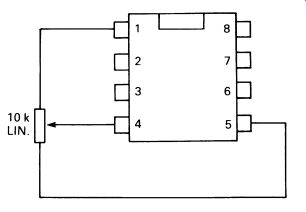
FIG. 4 offset null setting for the SN12741
Despite the usefulness and wide application of the op-amp, there will be many occasions when the engineer will want to design an amplifier using discrete components. There will be even more occasions when the service engineer will meet other types of amplifier. But the study of operational amplifiers is important because the general principles of design particularly in feedback circuits-applies to virtually every amplifier design.
1. NEGATNE FEEDBACK TECHNIQUES
First of all, we need some control over that (almost) infinite gain! Fig. 5 illustrates the basic op-amp configuration with feedback.
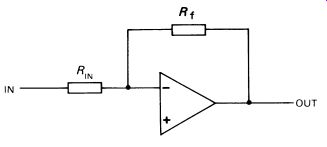
FIG. 5 the basic op-amp feedback configuration, using the inverting
input
Assuming that the amplifier really does have infinite gain, the gain is controlled only by the values of the resistors RIN and Rr. RIN is the input resistor, and must be substantially less than the input resistance of the op amp. Rr is the feedback resistor. The voltage gain of the system is very simply calculated as:
A= Rr RIN
where A is the voltage gain. The fact that the op-amp has finite gain affects the calculation only slightly, provided the required gain is not approaching the specified maximum of 100dB or so. Fig. 6a is a practical circuit. Notice the odd power-supply requirements. The SN72741 needs a power supply that is symmetrical about zero. This permits the output voltage to swing above and below zero. There are various ways of contriving such a supply, but the simplest (and good enough for our purposes) is to use two 9 V batteries (PP3 or PP9) wired as shown in Fig. 6b.
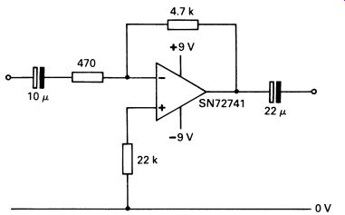
FIG. 6 (a) a practical amplifier based on the circuit of Fig. 5 ; (b) a simple power supply that can be used for the amplifier in
Fig. 6a
Remember that the inverting input is relative to the non-inverting input, not to the 0 V supply line. In our simple amplifier we want the input to be relative to 0 V ('earth'), so we connect the non-inverting input to 0 V. This is best done via a resistor, though the value is uncritical 22 kOhm is convenient. This amplifier circuit has a gain of ten time (3 dB) set by the values of the input and feedback resistors, 4700/470. The capacitors are added for a.c. operation, and could be left out for low frequency applications, according to the input characteristics.
This amplifier is inverting. The design of a non-inverting amplifier is slightly more difficult, since although the input is applied to the non inverting input, the feedback still has to be applied to the inverting input.
The basic configuration is shown in Fig. 7.
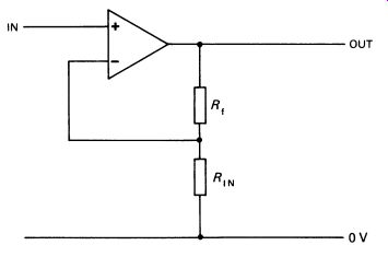
FIG. 7 the basic non-inverting configuration for the op-amp.
The gain of the non-inverting amplifier shown here is calculated as: A= RIN +Rr RIN A practical non-inverting amplifier with a gain of 11 is shown in Fig. 8. The capacitors are added for a.c. operation, as for the circuit in Fig. 6.
It is possible to apply several inputs to the op-amp configuration, isolating the inputs from one another with the input resistors, which should be as high in value as practicable-the higher they are, the better the isolation. Such a circuit could be used for an audio mixer, shown in Fig. 9. The input resistors R1 , R2 and R3 set the maximum gain of the channels; in this case, R1 and R2 give a gain of 10, and R 3 gives a gain of unity (no amplification). The logarithmic potentiometers give volume controls that are suitable for audio use-slider controls are more convenient to use than rotary ones.
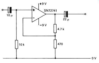
FIG. 8 a practical circuit based on the configuration in Fig. 7; the power supply in Fig. 6b can be used for this circuit
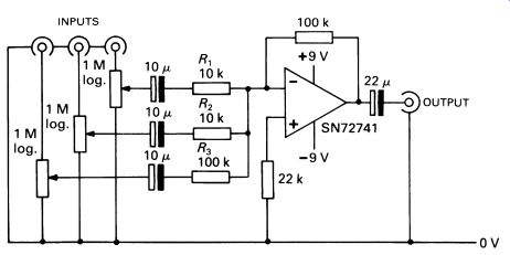
FIG. 9 a practical circuit for an audio mixer; an op-amp provides
amplification (the power-supply circuit of Fig. 6b can be used with
this design)
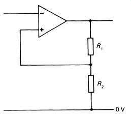
FIG. 10 an op-amp in a positive feedback configuration; note that
it is the non-inverting input that is connected to the junction of the
two resistors
2. POSITIVE FEEDBACK TECHNIQUES
It may appear at first that positive feedback-feedback that reinforces the input rather than reduces it-would not have a great deal of application to a very high gain operational amplifier. This is not in fact the case, and a whole class of circuits is based on positive feedback. Fig. 10 shows the basic configuration for positive feedback.
The similarity to Fig. 7 is superficial-compare the positions of the inverting and non-inverting inputs. Assume there is no output from the circuit, the output being exactly zero. If a small positive voltage is applied to the input, the output swings negative. The non-inverting input, previously held at zero volts through R 2 , is now provided with an amplified negative signal from the output, via R1. This reinforces the input by increasing the potential difference between the two inputs. The result is that the output swings very rapidly to its maximum negative excursion, just slightly away from the negative supply voltage.
If a sufficiently large negative potential is applied to the input, enough to make the output positive, even momentarily, the circuit will rapidly change state and the output will swing to its maximum positive excursion.
This is very like the bistable circuit of Section 10, in that the circuit can adopt one of two stable states: this is, in fact, an op-amp bistable. A practical circuit is shown in Fig. 11 , the only extra factor being the extra resistor to ensure that the inverting input remains at zero volts in the absence of an applied signal.
An adaptation of this circuit can be used as a perfectly usable touch switch, to turn a lamp on or off. Fig. 12 provides a suitable circuit.
The touch contacts are illustrated in Fig. 13 and can be made with drawing-pins. The resistance across a human thumb is about 50 k-Ohm to 2 M-ohm, depending on the dryness of the skin, and this allows enough current to flow to make the circuit change state. The tiny current is, of course, completely harmless, but the circuit must be used only with battery power or with a correctly designed and isolated power supply. The diode is necessary to ensure that the lamp lights only when the output of the amplifier is negative; without the diode, the lamp would light all the time.
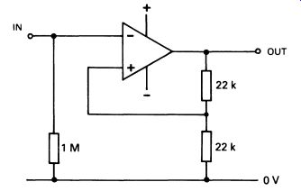
FIG. 11 a practical circuit for an op-amp bistable
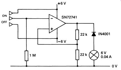
FIG. 12 a practical design using the circuit of Fig. 11 that
operates as a touch-sensitive switch to turn a lamp on or off; if the
circuit is required to switch a high voltage or current, the lamp can
be replaced with a relay (see Section 17)
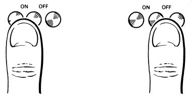
FIG. 13 suggested layout for the switch for Fig. 12
3. OPERATIONAL AMPLIFIER OSCILLATORS
In Section 10 we developed the bistable multivibrator into an astable.
There is a parallel with the op-amp. Fig. 14 shows a basic op-amp oscillator.
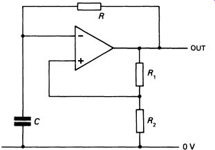
FIG. 14 an op-amp oscillator
The principle is straightforward. Starting with the amplifier in a condition where the output is positive, the capacitor C is charged, via R, until the inverting input becomes sufficiently positive to cause the 'bistable' to change state, the output now becoming negative. It is now a negative potential that is applied to C, via R, and C is discharged and recharged with the other polarity. When the potential on the inverting input charges, the 'bistable' again changes state; and so on. The calculation for the rate at which the circuit changes state is given by the following formula, where T is the total time taken for the oscillator to go through one complete cycle:
T= 2RCln (1 + ~~)
(ln is the natural logarithm, log to the base e). Fig. 15 gives a practical circuit to demonstrate the op-amp astable, with a simple transistor amplifier to increase the output volume.
The variable resistor allows you to adjust the output over a range of audio frequencies. The output of the circuit is approximately a square wave (Fig. 16).
FIG. 15 a practical circuit enabling the op-amp oscillator to drive a small speaker; the operating frequency of the oscillator can be adjusted by means of a variable resistor
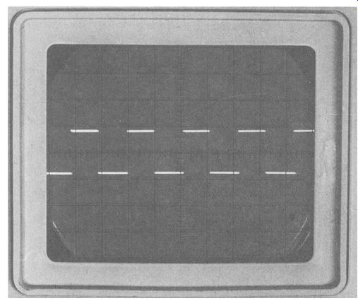
FIG. 16 the output of the oscillator in Fig. 15
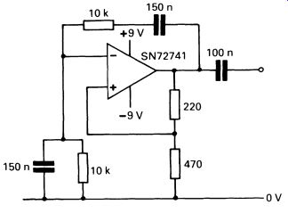
FIG. 17 the Wien bridge oscillator is used where a sinewave output
is required

FIG. 18 the output of the Wien bridge oscillator
One type of oscillator that produces a sinewave output is the Wien bridge oscillator. This circuit is shown in Fig. 1 7. This circuit has two Rs and two Cs, which makes frequency adjustment difficult. A dual 10 k-Ohm potentiometer can be used. The frequency of operation is given by:
F=-t7TRC
where F is the frequency in hertz. Fig. 18 gives the output waveform.
4. CONTROL OF FREQUENCY RESPONSE
By putting frequency-sensitive components or networks in the feedback loop, the frequency response of the op-amp can be controlled. If the feed back resistor Rr in Fig. 5 is replaced by a capacitor, then the op-amp will act as a low-pass filter. As high frequencies pass through the capacitor more readily than low frequencies, the feedback is greater at high frequencies and the gain lower.
A resistor and capacitor in parallel, used in the feedback loop--Fig. 19--will cause the amplifier to amplify a selected frequency, with the gain falling off above and below the center frequency. The same formula that we used for the Wien bridge oscillator (F = -!-1rRC) gives the center frequency, the frequency at which the amplifier exhibits the highest gain.
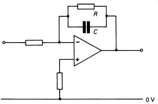
FIG. 19 the frequency response of the op-amp can be controlled by
means of frequency-sensitive components in the feedback loop
QUESTIONS
1. Give the ideal specification of an operational amplifier in terms of (i) gain, (ii) input resistance, (iii) output resistance, (iv) bandwidth.
2. Draw circuit diagrams for an op-amp using (i) negative feedback, (ii) positive feedback, providing a bistable circuit.
3. Draw circuit diagrams for (i) inverting, (ii) non-inverting amplifiers using op-amps. In both cases show resistor values to give a gain of 25.
4. Draw a circuit (omit component values) for an op-amp astable circuit.
5. What is meant by 'common mode rejection ratio'?