AMAZON multi-meters discounts AMAZON oscilloscope discounts
Section 7 covered the basic physics of semiconductor devices, and just touched on the methods used to manufacture the components themselves.
Semiconductor manufacture, or 'fabrication' as it is more generally called in the industry, is a highly specialized and very difficult subject, but it is useful for the electronics engineer or technician to have some idea of the principles involved.
Various different semiconductor materials are used, but the most common (and cheapest) is silicon. In this section we shall look at the fabrication of semiconductor devices based on silicon, but you should bear in mind that roughly similar techniques--although with different materials-are used to deal with germanium and the other semiconductors.
1. PURE AND VERY PURE ...
The first step is to take a single large crystal of pure silicon. This is not as easy as it seems, for silicon that only thirty years ago would have been called 'chemically pure' would be hopelessly contaminated for the purpose of semiconductor manufacture. In the early days of transistor manufacture (1960s) the purity of the raw material, usually germanium, was the major obstacle to reliable production. A process that had worked perfectly for weeks would suddenly start turning out 100 percent rejects, and would have to be stopped. The batch of semiconductors would be thrown out, everything cleaned, and (with luck) the process might be restored to correct operation after a month. This sort of thing was one of the main reasons for the high cost of early transistors. Today, manufacturers of semiconductor grade silicon aim for no impurity atoms at all. This level is never reached, but crystals having impurities less than 1 part in 1 000 000 000 are routinely made.
One way of making pure silicon crystals was described at the end of Section 6. We begin with the sausage-shaped single crystal of silicon that is drawn out of the pure silicon 'melt'.
The silicon crystal is sliced up (like salami) into circular wafers, typically 50mm diameter and 0.5 mm thick. The surfaces are ground and polished perfectly flat, leaving the wafer about 0.2 mm thick. The wafer is finally cleaned with chemical cleaners.
The technique for making a single pn diode is as follows.
Beginning with a wafer of p -type silicon, made by adding a tiny amount of p- type impurity such as indium or boron to the pure silicon, an n-type epitaxial layer about 15 um thick is 'grown' on the wafer. This is done by heating the wafer to about 1200°C in an atmosphere of silicon and hydrogen tetrachloride with a trace of antimony, phosphorus or arsenic. Next a thin (about 0.5 um) layer of silicon dioxide is grown on top of the wafer by heating it to about 1000°C in an atmosphere of oxygen or steam.
Silicon dioxide has three very useful properties. It is chemically rather inert and is not attacked by gases in the atmosphere, or indeed most other chemicals, even at high temperatures. Second, it is impervious and prevents the diffusion of impurities through it. Third, it is an excellent electrical insulator. The wafer at this stage is shown in cross-section in Fig. 1.
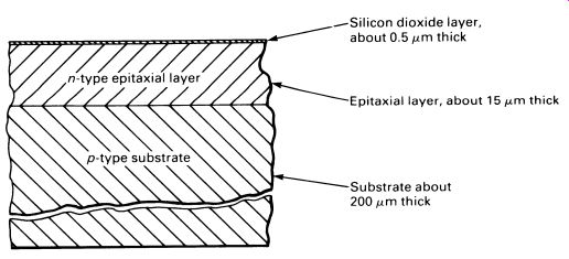
FIG. 1 silicon wafer in cross-section, after formation of a silicon
dioxide layer on its surface.
Next, openings have to be made in the silicon dioxide layer, in the right places. This is done photographically. The wafer is coated with a photoresist, a light-sensitive emulsion similar to the emulsion on a black· and-white film. A pattern, having the necessary cutouts, is placed over the photoresist, and the wafer is exposed to powerful ultraviolet light. The pattern, or mask, is removed, and the wafer washed with trichloroethylene, a chemical that dissolves the photoresist only in the places where it was not exposed to the ultraviolet light. This leaves the photoresist as a 'negative' of the mask.
At the end of this stage, the wafer is washed in hydrofluoric acid, a very powerful acid that will actually dissolve glass-but not the special photo resist (nor, fortunately, the silicon wafer!). The wafer is washed again, and the resist removed with hot sulphuric acid. The various steps are shown in Fig. 2.
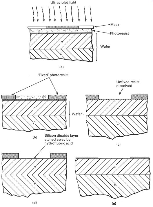
FIG. 2 the various stages in masking and etching the silicon dioxide
layer.
The end-result of this procedure is to produce the right pattern of holes in the silicon dioxide layer. Our wafer now goes back in the furnace, with an atmosphere of p -type impurity. The impurity diffuses into the wafer below the holes in the silicon dioxide, but nowhere else (see Fig. 3). Fig 3 p-type impurity is diffused into the upper n-type layer The whole process is repeated, with a different mask, to diffuse another n-region into the p-region just created. Then the whole process is repeated a third and then a fourth time, to diffuse more doped regions into the wafer. Fig. 4 shows the final result.
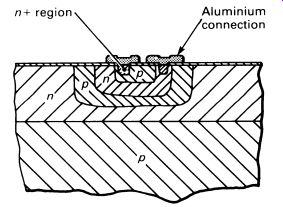
FIG. 4 a completed silicon planar epitaxial pn diode.
Connections have been made to the heavily doped n+ regions, by evaporating an aluminum film on to the wafer, after suitable masking. If this seems a terribly complicated way of making a pn diode (compare Figure 7. 7, p. 84, with Fig. 4, for example) then it is for a reason.
Those extra p and n layers below the diode itself-the pn junction connected to the outside world-serve to isolate the diode from the rest of the wafer. A reverse-biased pn junction surrounds all parts of the diode, preventing leakage to the rest of the wafer. Now this is not a very useful feature if we are going to cut the wafer up into individual diode chips.
But suppose we cut the wafer into larger sections? The aluminum layer could carry current from one part of the wafer to another, and transistors and diodes could all be combined on a single chip to build a complete circuit! And this idea is the basis of microelectronics. The first integrated circuits used just this technique, though more recent devices are rather more subtle, and rely on electrical connections inside the silicon structure rather than on superimposed aluminum 'wiring'.
2. INTEGRATED CIRCUITS
Diodes and transistors-bipolar and FETs-can be produced on a silicon wafer. So, too, can resistors, either deposited on top of the wafer in the form of tantalum (a poor conductor), or built into the wafer as a 'pinch' resistor. The pinch effect is similar to that observed in a partially turned off FET and relies on a very thin region for conduction. Resistance values of up to 100 k-Ohm can be produced in this way.
Capacitors are more problematic, and although it is possible to make capacitors on an integrated circuit, the values are generally limited to a few picofarads if the capacitor region is not to be excessively large. Capacitors are to be avoided in integrated circuits as far as possible.
There is no equivalent of an inductor, but fortunately most circuits can be designed to avoid this requirement.
3. TESTING AND PACKAGING
The silicon wafer may eventually contain several hundred complete integrated circuits. They are, of course, all produced simultaneously, the masks used during processing consisting of hundreds of identical units. See Fig. 5.
It is usual to test the individual circuits before the wafer is cut up.
Testing is done automatically, and the machine marks any faulty circuits with a blob of ink. The yield, i.e. the percentage of 'good' circuits, varies considerably. Complex circuits might have a yield as low as only a few percent, whereas simple circuits would be much better. The reason is clear-if a number of faults are scattered over a wafer, the larger the number of circuits on that wafer, the more fault-free circuits there will be.
Once the wafer has been tested, it is cut up and the faulty circuits discarded, again automatically. The chip is mounted on a suitable frame, and connections are made between the aluminum 'pads' on the chip and the frame which forms the connections to the chip. The chip is still usually hand-wired to the frame, using ultrasonic welding to make the connections. The work is done under a binocular microscope, using special micro-manipulators. Fine gold wire is often used for the connections. Fig. 6 illustrates the first part of the process.
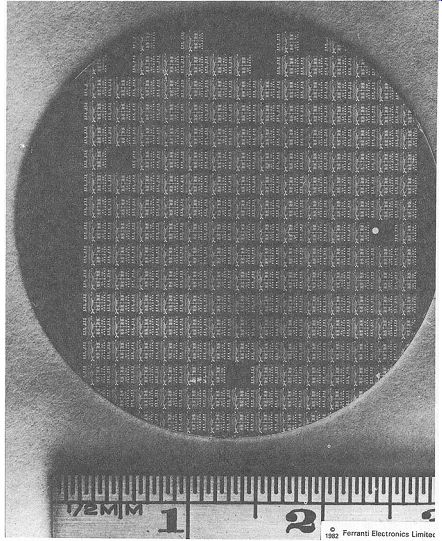
FIG. 5 a silicon wafer-with a ruler to indicate the scale-showing
a little under 200 individual integrated circuits, ready to be tested
and cut up
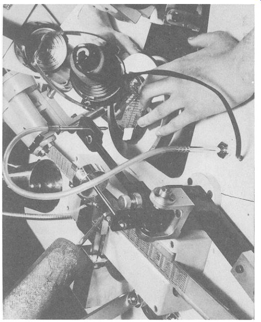
Fig 6 mounting individual silicon chips in their frames,
prior to adding the connections and encapsulation
Various styles of encapsulation are used, but by far the most common is the DIL pack (Dual-In-Line). DIL packs are based on a standard to inch matrix. The pins down each side are always 0.1 inch apart, and the distance between the two rows of pins is a multiple of 0.1 inch, generally 0.3 inches for packages of eighteen pins or less, and 0.6 inches for twenty pins or more. Fig. 7 illustrates typical plastic DIL packs.
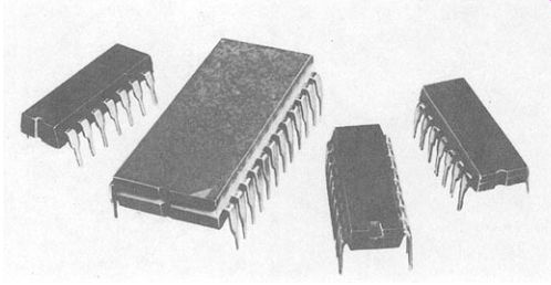
FIG. 7 a selection of DIL-packs, the form in which integrated circuits
are generally sold Ceramic DIL packs are used as well as the plastic
ones, but only for the most expensive devices, or those requiring a very
high degree of environ mental protection. The number of individual semiconductor
devices that can be packed on to a single chip is astonishing. Although
a 14-pin DIL pack may contain a relatively simple circuit (see below)
a 40-pin DIL pack can contain the electronics for a complete computer!
Fig. 8 shows a complex integrated circuit. It is in fact the central
processor unit of a computer. Devices like this have a huge number of
transistors and diodes, approaching 10000 on a chip less than 10mm square.
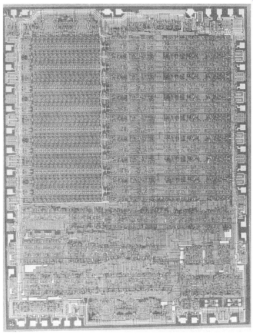
FIG. 8 an example of a large-scale integrated circuit, a microprocessor;
this IC contains all the important parts of a computer central processor
unit
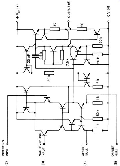
FIG. 9 circuit diagram of a typical bipolar IC, operational amplifier
type SN72741
4. SOME EXAMPLES OF SIMPLE INTEGRATED CIRCUITS
In the next section we shall look at operational amplifiers, so it seems sensible to take one of the most popular operational amplifiers as an example of the kind of circuit design used (see Fig. 9). This is the operational amplifier type SN72741. As you can see, there are many transistors, a few resistors (they take up more room on the chip than transistors or diodes), and as few capacitors as possible (one). But this is a relatively simple circuit; it is very cheap, currently costing less than a cup of coffee.
Such is the scale of mass production in the microelectronics industry! The second example-in Fig. 10--relates to Section 19, and shows a 2-input AND gate. A 14-pin DIL pack contains a chip with four such gates.
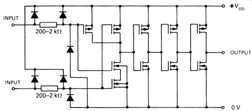
FIG. 10 a typical simple IC using MOSFET technology; components
can be packed up to twenty times more densely than with bipolar technology
(this diagram shows one of four identical circuits included in the CD4082
quad 2-input AND gate).
The use of MOSFET technology means greater economy, as it can be packed on the chip up to twenty times more densely than bipolar transistors. Also, the power requirements are much lower. The CD4082 quad 2-input AND gate is as cheap as the SN72741 operational amplifier.
More complicated chips, such as the Z80 microprocessor, are more expensive, but still amazingly cheap. The Z80 currently costs about the same as a pound of coffee beans.
QUESTIONS
1. Why would a complex IC have a lower production 'yield' than a simple one?
2. What method is used to manufacture pure silicon such as might be used for semiconductor manufacture?
3. Silicon dioxide layers feature prominently in the manufacture of all silicon semiconductor devices. What are important properties of silicon dioxide?
4. What is the pin spacing of the standard DIL pack?
5. Name two 'impurity' materials that are added to pure silicon to produce (i) n -type, (ii) p -type silicon.