AMAZON multi-meters discounts AMAZON oscilloscope discounts
Counting circuits are among the most important of all sub-systems, and are used in a tremendous variety of electronic equipment. People unused to electronics often fail to appreciate just how fast an electronic counting circuit can work. A typical TTL counter might accept a count frequency of 30 MHz. You only begin to realize the speed of this when you compare it with other things that are normally considered very fast. Imagine you have a revolver, and that a counter working at 30 MHz is connected in such a way that it begins to count the instant the firing pin hits the cartridge.
Fire the pistol and watch the counter-if you have good eyesight you will notice that the counter reaches a count of around 10 000 before the bullet emerges from the end of the pistol's barrel! Electronic counters can also work slowly, but the potential for such rapid counting opens the way for all sorts of useful designs.
Before the advent of integrated circuits, counting circuits were rather complicated and difficult to build. Electronics technicians and designers needed a detailed knowledge of many types of counting circuit, mostly based on the transistor bistable configuration, but some based on special 'counting tubes'. For low-speed operation, mechanical counters worked by electromagnets were often the best answer.
The position is very different nowadays. Many types of counter are available in integrated circuit form, and it is not really essential to know in detail what goes on inside the circuit. Indeed, manufacturers with an original circuit design are often reluctant to publish details. What we do need is a clear idea of the various forms of counter, what their limitations are, and how they can be used.
1. THE BISTABLE
The bistable is one of the simpler circuit elements. Before the integrated circuit era, the bistable circuit had to be made up from discrete components, and required, in its simplest form, two transistors and four resistors. The circuit is given in Fig. 1.
Imagine that TR 1 is conducting, so that TR 1 has a very low resistance.
Point 'X' in the circuit will be near to 0 V (disregarding the forward voltage drop of the junction of the transistor). The base of TR2 is held at this level via R2 , and since the transistors in this circuit are of the npn type, TR2 is turned off. Point 'Y' is therefore at a high potential, and this high potential is applied to the TR 1 base, keeping TR 1 turned on. The circuit is completely stable in this condition and will remain indefinitely with TR 1 on and TR2 off.
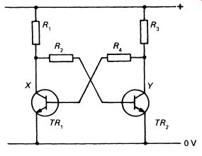
FIG. 1 the simplest transistor bistable requires six discrete components
But the circuit is symmetrical. Both 'sides' are identical, and it will be equally stable with TR 1 off and TR2 on (hence the name 'bistable'). The bistable can be made to switch states by the application of a suit able voltage to the base of one or other of the transistors. If TR 1 is on, a brief pulse of positive voltage to the base of TR2 will turn on TR2 instead, switching TR 1 off. A simple demonstration circuit is easy to make, and Fig. 2 gives all the information needed. LEDs are connected in the two collector circuits to show which transistor is switched on. Momentary connection of terminal T1 or T2 to the positive supply will switch on the associated transistor, and switch off the other one.
More simply, bi-stables can be made using NOR gates. The circuit shown in Fig. 3a (p. 300) performs in the same way as the discrete component version in Fig. 2, the section shown dashed is required only in the demonstration circuit to indicate which state the circuit has adopted.
Once again, it is quite simple to build the demonstration circuit. Details are given in Fig. 3b.
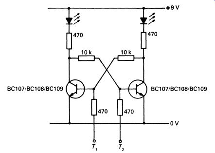
FIG. 2 a practical transistor bistable, suitable for demonstration
purposes; component tolerances are uncritical, and most npn transistors
will work satisfactorily in this circuit (red LEDs make useful indicators
to show which transistor is on)
2. INTEGRA TED CIRCUIT FLIP-FLOPS
Purpose-built bistable ICs are also available. A bistable similar to that in Fig. 3a is termed an S-R flip-flop (the S-R standing for SET-RESET). The circuit symbol for this is given in Fig. 4.
When S is 1 and R = 0, Q is also 1 , and Q is 0. When S is 0 and R is 1 , the circuit changes state and Q becomes 0 and Q becomes 1. If both Sand R are 0 or 1, the circuit will remain in the state in which it was last set.
Put simply, a logic 1 on either the S or R input makes the circuit flip (or flop) over to the Q or Q output respectively.
The third input is the clock input, CK. If both Sand R are at logic 1, a 1 pulse applied to the CK input will cause the circuit to change state (Q and Q becoming 0 and 1 or 1 and 0). Each successive clock pulse-a swing from 0 to 1 and back again-will make the circuit change state. It is usual (but not universal) for the circuit to change state as the clock pulse falls from 1 to 0. Fig. 5 shows the clock input, and the way the output changes state.
The CLR (clear) input has to be held at logic 1 for normal operation. It is taken to 0 to reset the bistable, which makes Q go to logic 0, Q to 1 , and suppresses all further changes of state. The various combinations of inputs and outputs are shown in the table in Fig. 6.
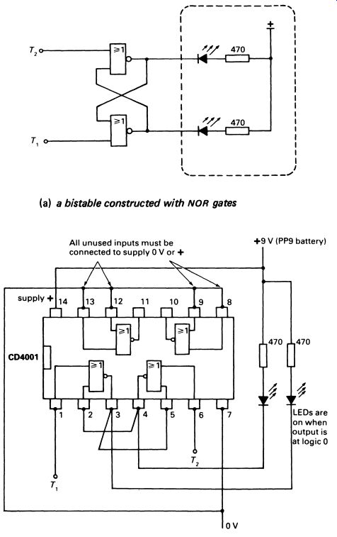
FIG. 3 (a) a bistable constructed with NOR gates (b) a demonstration
NOR gate bistable, with LED indicators to show the state of the circuit:
a CD4001 integrated circuit is used, and a 9 V PP3 battery provides the
power source
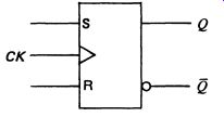
FIG. 4 S-R flip-flop symbol
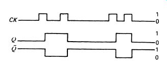
FIG. 5 clock and output waveforms of the flip-flop
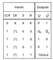
FIG. 6 function table for the S-R flip-flop X = doesn't matter Q0,
Q0 = outputs remain in the state they were in before the indicated input
conditions were established TOGGLE = Q and Q change state n. = clock
pulse rises from 0 to 1 and falls to 0 again
Fig. 7 shows another more complicated type of bistable called a J-K master-slave flip-flop. This consists of a pair of S-R flip-flops, connected together by various logic gates. The input gates are connected to the outputs, so that the J and K outputs are in the opposite state. This ensures correct operation of the circuit under most conditions.
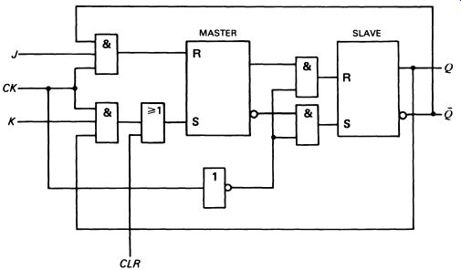
FIG. 7 master-slave J-K flip-flop logic diagram
The circuit illustrated is a real device, type SN74107, which has two identical J-K master-slave bistables in a single 14-pin package-illustrated in Fig. 8.
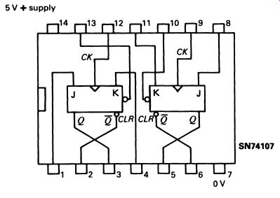
FIG. 8 a TTL dual master-slave J-K flip-flop, the SN74107
Although the master-slave arrangement appears unnecessarily complicated, it differs from the simpler arrangement in an important respect. If the clock pulse is at logic 1, a logic 1 applied to J or K will not affect the outputs. However, new data are accepted by the master. When the clock pulse returns to logic 0, the master is isolated from the inputs but its data are transferred to the slave, and Q and Q can change state. In a system incorporating several such flip-flops, this gives the important advantage that they all change state simultaneously.
3. BINARY COUNTERS
It is clear from Fig. 5 that a single flip-flop actually divides by two: the waveform from Q (or Q) is at half the frequency of the clock. The circuit is actually 'counting' up to two. We can wire the two flip-flops in the SN7473 together, as shown in Fig. 9.
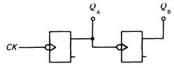
FIG. 9 two flip-flops connected to provide a binary count of 0 to
3
It is understood, when drawing logic diagrams like this one, that terminals not shown are connected to the right logic levels for the circuit to operate correctly-/, K and CLR are all taken to logic 1, and of course the circuit's power supply has to be connected. The output of this configuration is illustrated in Fig. 10. Follow the logic by looking at the two figures.
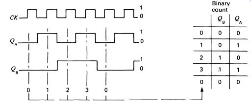
FIG. 10 clock and output waveforms of the two flip-flops shown in
figure 9; the table shows the derivation of the binary count
This circuit has divided by two twice, or divided the input frequency by four. Also, if we look at the logic levels at QA and Q8 we can see that the outputs have provided a count of 0 to 3 in binary. After 3, the counter goes through the cycle again. Each stage doubles the size of the count, so that three stages would count up to 8. and four stages would count up to 16 (including the zero). Four-stage binary counters are available all in one package, such as the SN7 493 shown in Fig. 11.
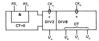
FIG. 11 a typical TTL four-stage binary counter, the SN7493
There are two clock inputs in this integrated circuit: CKA is the normal one used, but CK 8 , connected to the second flip- flop in the chain, is provided because the QA output is not connected to the clock input of the second flip-flop. This gives the user the choice of a three- or four-stage counter; for four-stage operation QA is connected externally to CK8 . The two RS inputs are used to reset the counter (all outputs to logic 0); both RS inputs have to be high to cause reset to take place. These various alternatives are 'designed in' to the integrated circuit to make it as flexible as possible. It makes economic sense for a manufacturer of ICs to aim at the largest possible market! There are many more types of flip-flop, but perhaps the only other really important one to consider here is the D- type flip-flop (D stands for data). The D-type flip-flop has only one input apart from the clock, and this is connected to the J and K inputs as shown in Fig. 12.
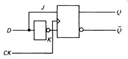
FIG. 12 input connections of the D-type flip-flop
The inverter in the K line ensures that the J and K inputs are always different from each other. A logic 0 or 1 on the data input will flip (or flop) the outputs when the clock pulse is at logic 0. The D-type can also be persuaded to toggle, by connecting it as shown in Fig. 13.
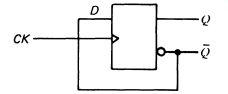
FIG. 13 connection required to make the D-type flip-flop toggle
with the clock pulses
Typical of TTLD-type flip-flops is the SN7474, shown in Fig. 14, which has two flip-flops in the same package. The 'preset' input is the complement of the 'clear' input, and sets the outputs to the opposite state.
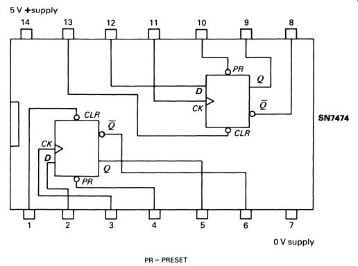
FIG. 14 a typical TTL dual D-type flip-flop, the SN7474.
Binary counters have many uses, but sometimes it is better to have a counter with a suitable output for ordinary denary (tens) counting.
Counters of this kind use ordinary flip-flops for the actual counting, with a system of logic gates to stop the count at nine. Typical of this sort of counter is the SN7490 decade counter. It has four outputs-the output is still in binary-and the sequence of counting is called binary coded decimal (BCD) meaning that the count is in binary but stops at nine.
The BCD output can be converted to a useful 'one often' output-ten lines, all at logic 0 except one. The one that is at logic 1 steps along the row for each count. To perform the conversion, a circuit called a BCD to decimal decoder is used: it has four inputs and ten outputs. A typical TTL circuit of this type is the SN74141. A popular example of a 'one-chip' decade counter--CMOS this time--is the CD4017. This is illustrated in Fig. 15a. The circuit in Fig. 15b makes an interesting demonstration of this type of counter. The LED display can either be made from separate LEDs, or with a 10-segment LED bar display like the one illustrated in Section 16 (p. 235). Provided the batter is not more than 9 V, no current limiting resistors are needed, the output current limitation of the CMOS gates being sufficient to ensure safe operation.
Decade counters, along with their associated decoders, can be 'chained' to provide counting and a digital display of the count. Each stage's nine count is used to clock the following stage to provide the carry to the tens, hundreds and thousands counters (and so on, if more stages are used). Alternative output decoders produce a suitable combination of outputs to drive a 7-segment LED display or LCD.
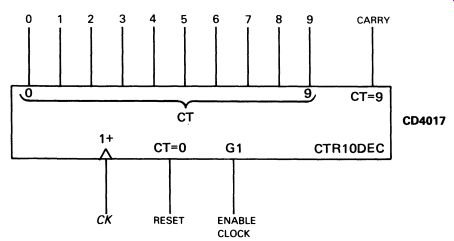
FIG. 15 -------- RESET: Normally at logic 0; when at logic 1, this
resets the counter (zero output high) and prevents the counter operating
ENABLE CLOCK: Normally at logic 0; if at logic 1, clock pulses have
no effect on count CARRY: Long pulse, goes from logic 0 to logic 1
as count goes from 9 to 0; used instead of 9 output for 'chaining'
counters (a) a CMOS decade (one-of-ten) counter
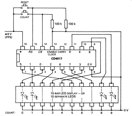
FIG. 15 cont. (b) circuit for demonstrating the decade counter;
only one of the LED segments is lit at any time, the segment corresponding
to the count; pressing RESET sets the count to zero, and each successive
press of the COUNT button advances the count by one; if the switch does
not operate 'cleanly', contact bounce may cause the count to advance
several steps (try using different switches); the supply voltage of
9 V should not be exceeded with this circuit, since there are no external
limiting resistors for the LEDs
4. LATCHES
It is often useful to 'freeze' the display while allowing the counter to go on counting. This may be essential to check the total of a fast counter without interrupting the count. A circuit known as a latch is needed for this. A latch has four inputs and four outputs. Normally the four outputs assume the same state as the inputs, but when a control input (known as the strobe input) is taken to logic 1, the outputs are locked in whatever logic state they were in at the instant of the strobe input going high. This enables the display to be frozen, without affecting the counter(s). A TTL circuit of this type is the SN7475 quad bistable latch.
As you might expect, it is possible to combine the BCD counter, latch and decoder on a single IC, which saves wiring and simplifies the construction of a complete counter system. The SN74143 illustrated in Fig. 16 is a good example of this type of integrated circuit.
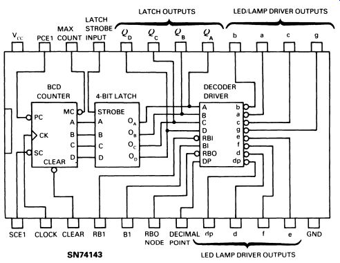
FIG. 16 a TTL BCD counter/latch/decoder circuit, the SN74143
5. SYNCHRONOUS COUNTERS
The simple binary counter illustrated in Fig. 9 is usually described as an asynchronous or 'ripple-through' counter. The reason is that it takes a certain amount of time for each stage of the counter to operate, and the more stages there are, the longer it is before the clock pulse has propagated through the system and all the outputs have settled down to their steady state values. There are various problems associated with this mode of operation. If you are designing a high-speed system, it is essential to know exactly when each switching takes place, or else logic sequences can get out of step; this can cause instability which prevents an apparently sound design from working.
A counter that works in a more predictable way is the synchronous counter. Synchronous counters have the counting sequence controlled by a clock pulse, all the outputs of the flip-flops changing state simultaneously (or synchronously). Synchronous counters are quite complicated, and involve gating the inputs of an array of J-K master-slave flip-flops. Outwardly its operation looks the same as an asynchronous counter, apart from the fact that all changes in the outputs take place as the clock pulse falls to logic 0.
6. UP-DOWN COUNTERS
Counters are also available to count up (add to the count) or count down (subtract from the count). Such counters feature an UP/DOWN control input which determines which way the counter works, according to the logic state applied to it.
7. CMOS COUNTERS
Because most of the circuits so far considered are from the TTL family, you might think that CMOS counters are less common. This is not the case, and there are CMOS counterparts (with slight variations) for all the types discussed already. For medium- and low-speed operation-up to 5 MHz-the advantages of CMOS counters are considerable. The low power requirements, wide power-supply voltage tolerance and excellent noise immunity make CMOS the first choice for low-speed/low-cost applications-and incidentally for easy and reliable demonstrations!
8. SHFT REGISTERS
A shift register is in many ways similar to a multi-stage counter, but it is used to store binary data and to 'shift' the data to the right or left along a row of output lines. Shift registers form an important part of all computers. Fig. 17 shows a typical four-stage shift register (CMOS) the CD4015 contains two identical registers.
This type of shift register is known as a serial-in, parallel-out design, and it works like this. When the clock pulse ( CK) goes to logic 1, the logic level currently on the DATA input is transferred to Q1 • The next clock pulse also 'reads' the data input and transfers it to Q1 , and the logic level previously present on Q1 is shifted to Q2 • The third clock pulse reads the data input again, sets Q1 to the corresponding logic level, and shifts the old data on Q1 to Q2 , and that on Q2 to Q3 • Each new clock pulse shifts the data one place to the right. At the end of the register (Q4 in this case) data are lost. It is possible to connect shift registers together to add stages-progress of data through an eight-stage shift register (such as could be made using the two halves of the CD4015) is charted in Fig. 18. The RS (reset) input allows the register to be reset, making all the outputs logic 0 (see Fig. 17).
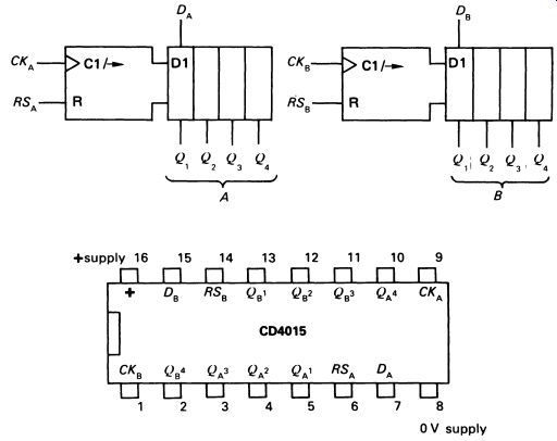
FIG. 17 a CMOS dual four-stage shift register, the CD4015
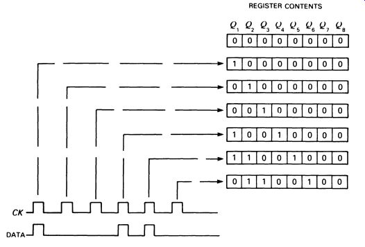
FIG. 18 the passage of data through an eight-stage shift register
There are many variations in shift register types. Some are serial-in, serial-out, and simply accept an input, which appears at the output after a fixed number of clock cycles-they are like the one shown in Fig. 16 but with only the Q4 output. Others have a parallel-in facility, by means of which data can be loaded into the register by applying them to a number of inputs (one for each stage) simultaneously. Still others are bidirectional and can shift data either way according to the logic level applied to a control input.
9. INTEGRATED CIRCUITS FOR COUNTING
Finally, it must be made clear that there are a large number of different kinds of ICs for counting in both major logic families, and many special purpose counting ICs using PMOS or NMOS techniques. Most are variations on the basic type of counters, shift registers, latches and decoders described in this section, and many are combinations of these circuits.
One thing is certain. These days it is very unlikely that anyone will have to design a counter circuit using discrete components. The current range of ICs is so large, and the individual devices so cheap, that 'doing it the hard way' would hardly ever be justified. When selecting an IC--particularly a counter or shift register--it is important to read the manufacturer's data-sheet carefully. All relevant specifications and parameters should be listed in great detail. Systems that refuse to work are often the result of mistakes in reading the data-sheet, or of not bothering to read the data sheet at all.
QUESTIONS
1. Give another name for the flip-flop.
2. An electronic stop-watch would probably incorporate latch circuits.
Describe the function of a latch.
3. The following data are applied to an 8-bit shift register:
0 0 1 1 0 1 0 1
What data would be present after three clock pulses, assuming the input remains at logic 0?
4. Sketch a system diagram for a TTL 0 to 9 counter, driving a 7 -segment LED display.
5. What are the functions of the CLEAR and SET lines of a counter IC?