AMAZON multi-meters discounts AMAZON oscilloscope discounts
Every counting circuit has to start with a circuit to generate pulses to count. Rarely, the pulses may be produced by some source outside the circuitry, for instance when counting events. More usually, the pulses are generated by special pulse-generator or timing circuits.
This section begins by looking at various methods by which pulses suitable for digital systems can be produced, and then goes on to consider the design of a 'real-life' digital system, as an example of the way digital systems are put together from gates and other commonly available ICs.
1. TIMERS
Although timers can be developed from discrete components, it is usual to design this part of the system using ICs. The most commonly used timer circuit is the NE555, packaged in an 8-pin DIL pack and sold for the price of a cup of coffee. The NE555 is quite an elderly design, and has a more modern variant, the ICM7555 of 'low-power 555'. The latter uses CMOS technology instead of bipolar, and operates with about one hundredth of the supply current; otherwise, the two ICs are identical.
The NE555 can be replaced directly with the ICM7555, but the reverse is not necessarily true. The package and pin connections are given in Fig. 1.
The NE55/ICM7555 ('55' for short in this section, and often in the industry) is very versatile, and can be used as a monostable or as an astable.
Pins 1 and 8 are the power supplies. The functions of the other pins become clearer by reference to a diagram of the system inside the 555. This is illustrated in Fig. 2.
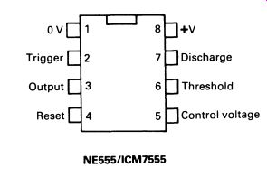
FIG. 1 a popular timer IC, the NE555
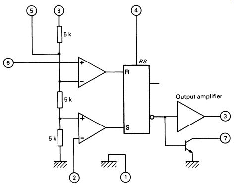
FIG. 2 System diagram of the internal circuitry of the NE555
The basic monostable configuration is given in Fig. 3. When the trigger is taken from + 5 V to 0 V (logic 1 to logic 0) the output will go high for a period determined by the values of R and C. The length of the output pulse is given as 1.1 RC seconds, so in the circuit of Fig. 3 will be 1.1 x (220 x 1000) x (100/1 000000000), which is 0.0242, or about 24 ms. The calculation can be made easier to remember if you use k-Ohm and 1-1F, and this provides an answer in milliseconds directly when used in the formula in place of R and C. In this circuit the timing sequence will continue even if the trigger is taken back to logic 1. To stop the timer, the reset input is taken from logic 1 to logic 0.
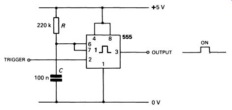
FIG. 3 the NE555 in a monostable configuration
Because the 555 can deliver currents of 100 mA or more, it is possible to use the 555 to drive a relay, for example, directly. However, precautions need to be taken to ensure that the back e.m.f. generated by the relay coil when the relay is switched off does not cause damage to the circuits. A diode placed across the coil in the 'opposite' direction to the current flow will absorb the induced high voltage. Where relays are packaged for use in digital circuits (for example, DIL reed relays) a diode is often connected across the coil inside the encapsulation.
The output of the 555 is, however, ideal for driving TTL or CMOS logic ICs, as it has a very rapid rise and fall, required for accurate timing and correct operation of some systems.
The 555 can be used in an astable mode, to generate a continuous train of pulses. The 'on' and 'off' times can be controlled separately, within certain limits. Fig. 4 shows a typical astable configuration.
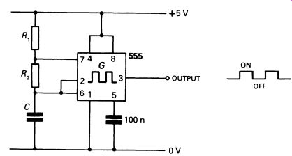
FIG. 4 the NE555 in an astable configuration
Note that the 100 nF capacitor connected to pin 5 is required for the NE555, but is not needed for the CMOS version-by reference to Fig. 2, can you see why?
The 'on' time (logic 1) is given by:
0.693(R1 +R2 )C
and the 'off' by:
so it is evident that the 'on' time must always exceed the 'off' time in this configuration, unless R 1 has a very low resistance compared with R 2 , in which case they can be about equal. The output sense can always be reversed (1 for 0) by the simple step of following the 555 with a TTL or CMOS inverter.
The 555 is very accurate, and is affected very little by temperature and voltage variations. The ICM7555 can be used with any supply voltage in the range 2-18 V, and timing accuracy changes by only about 50 parts per million per degree C. Maximum operating frequency is 500kHz, and the minimum frequency is determined only by the leakage of the capacitor used; one cycle per several hours is achievable.
Both TTL and CMOS logic gates can be used as timers, provided the frequency required is not too low. A simple CMOS monostable is shown in Fig. 5. The input to the inverter is normally held at logic 0 by resistor R. If the input is rapidly taken to logic 1, the input of the gate goes to logic 1 as well, and the output goes to logic 0. However, the capacitor now charges via R, since the left-hand side (in the diagram) is at logic 1 level. The charging rate is governed by R (assuming R to be at least a few kilohms), and the voltage across the capacitor drops at a controlled rate. When the voltage on the input of the gate drops to half the supply voltage, the gate changes state and the output goes high again.
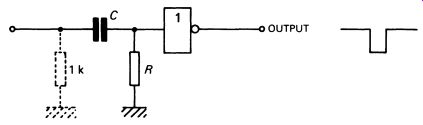
FIG. 5 a simple CMOS monostable
The shaping of the input and the requirement for an input resistor (1 k-Ohm in the diagram) to discharge the capacitor are taken care of if the circuit is preceded by another gate (see Fig. 6). With the input to the first gate at logic 1, the output is also a logic 1. If the input is taken to logic 0, the output is a logic 0 pulse, of duration 0.5 RC. Note that the input must be held at logic 0 throughout the duration of the output pulse. There will be no further output from the circuit until the input is taken back to logic 1 and then to logic 0 again.
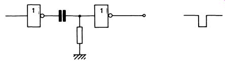
FIG. 6 the CMOS monostable is usually preceded by a CMOS gate, which
takes care of the correct input parameters
CMOS circuits may also be used to make astables. Fig. 7 illustrates the standard CMOS astable configuration. The time taken for one complete cycle of this astable circuit is approximately 1.4 RC, with a small variation according to supply voltage. The circuit is remarkably unaffected by temperature variations, and no temperature compensation will be required.
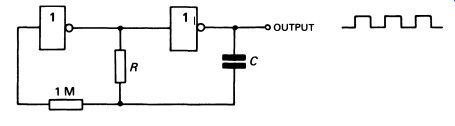
FIG. 7 a basic CMOS astable circuit
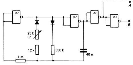
FIG. 8 a CMOS astable circuit that has independently variable 'on'
and 'off' times
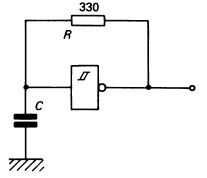
FIG. 9 a TTL astable configuration
It is possible to control the 'on and 'off' times independently by forcing the capacitor to charge and discharge through different resistors-easily done with diodes. The circuit of Fig. 8 provides an output pulse that can be varied from 1 to 2 ms, with a fixed interval between pulses of about 20ms.
It is possible to make similar circuits using TTL logic, though for timing applications a gate with a Schmitt input should be used. Normal TTL responds erratically to input signals that rise and fall slowly; the Schmitt input range of gates provides a rapid switching transition even when the input is a 'slow' rise or fall. A TTL astable design is shown in Fig. 9.
Although CMOS and TTL astables can be quite accurate, and some of the purpose-made timers are very accurate, their accuracy depends eventually on the performance of the resistor and capacitor used as timing elements. For some applications, such as clocks and watches or computer clock generators, this is not accurate enough. As we saw in Section 10, the most accurate form of oscillator in general use is the quartz crystal oscillator. A crystal-controlled oscillator can be made using a CMOS gate, as in the circuit of Fig. 10 overleaf. The crystal should not have an operating frequency of more than 3 MHz. The variable capacitor can be used for trimming the frequency within narrow limits.
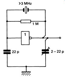
FIG. 10 a crystal oscillator circuit using a single CMOS gate
2. IMPLEMENTATION OF A DIGITAL SYSTEM
Traffic lights in Britain go through a sequence of green (go), amber (stop if you can), red (stop), red and amber (on your marks ... ), and back to green again. The design of a timing system to operate such traffic lights, even without radar control, car counters and other 'extras', turns out to be by no means trivial.
First, assuming that we have excluded systems of motors, cams and switches, we must choose the kind of technology. CMOS is probably the best, not because we are worried about power requirements, but because CMOS is less affected by electrical interference than is TTL. Also, CMOS happens to be a better bet for prototype demonstrations! Temperature range, -55 to 125 °C, should be satisfactory for Britain. It is essential to design the power supply to protect the circuits from transients in the power line (suppose the power-supply lines are struck by lightning?) and it is possible that this consideration alone could tip the scales in favor of TTL. Assume that we settle on CMOS. There are four possible configurations for the lights, shown in the table in Fig. 11.
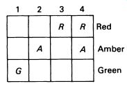
FIG. 11 truth table for UK traffic lights
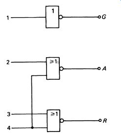
FIG. 12 a system of gates to implement the truth tables in Fig. 11
Three gates will 'translate' the four outputs into the right combinations of lights-two NOR gates and an inverter (see Fig. 12). Each of the four lines must go high in turn, so a counting circuit would almost certainly be the best bet-a CMOS CD4017 (see Fig. 21.15 ) seems ideal, except that there are too many output lines. The counter must be driven by timer, to 'clock' the count. The circuit given in Fig. 13 works.
Note the rather smart connection between output 4 and the RESET input: when the clock sends the CD4017 to a count of 5, output 4 goes high and makes RESET high as well, forcing the counter to reset back to zero, with line 0 high. This works with the CD40 17, but might not work with other counters, which need a longer pulse on RESET. In these cases a monostable needs to be fitted between the output and the RESET input.
It all depends on the internal organization of the IC.
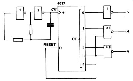
Fig 13 driving
the gates with a CD4017 counter.
The 555 generates clock pulses, to time the lights.
Drivers will have spotted the snag with the design--the lights need to be red or green much longer than they are amber or red and amber. Fig. 14 shows a sort of 'stop-gap' design, in which the lights are green or red for four times as long as they are amber or red and amber. It does this by making use of all ten output lines of the CD4017, plus larger NOR gates to decode the outputs. Operation is straightforward and should need no explanation beyond the circuit diagram.
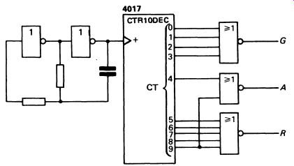
FIG. 14 using the counter to provide more realistic timings for
the lights
What is really needed is a system in which the timer's frequency is altered for each light-or perhaps separate timers for each of the four possible intervals. It turns out that the second idea is quite practical and relatively simple to implement. Fig. 15 illustrates a complete system.
This one does need explanation.
Assume that the circuit initially has output 0 high. The upper input line of the 4-input NOR gate (G1) is at logic 1, so the output of the gate G1 is at logic 0. After a period determined by the RC timing network (100 uF and 1 Mil) the input to G1 will drop to a point where it goes from logic 1 to logic 0. With all its inputs now at logic 0, G1 output goes high, applying a logic 1 to G2 input via the 4.7 nF capacitor; G2 output goes to logic 0 until the time constant 0.5 RC has elapsed (R = 120k-Ohm, C= 4.7 nF, gives around 250 us). At this point G2 output goes high again, and the leading edge of this pulse clocks the 4017 counter. Output 0 goes to logic 0, and now output 1 becomes logic 1.
The whole sequence is repeated, but with a different timing network, 4.7 uF and 1 Mil. The counter steps to outputs 2 and 3, and finally to 4, which forces a RESET and goes back to output 0.
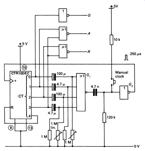
FIG. 15 a practical demonstration circuit giving independently variable
'on' times for red and green traffic lights
Three gates decode the outputs to operate three lights, as in the earlier system. In this design the amber and red and amber time constants are fixed at about 2.5 s. The green and red can be separately set up to approximately 50s.
As a working system this might or might not prove practical when fitted into real traffic lights. There is one design difficulty to be sorted out, too. If (after a power cut) the counter powers up with outputs 5, 6, 7, 8 or 9 high, there is no reason why the circuit should ever start. A manual clocking switch solves the problem for the experimental model, however, an automatic start-up would be needed in practice.
There is also the question of making the CMOS outputs drive three heavy-duty light bulbs. This would probably be done with triacs, and perhaps opto-isolators. Less impressively, LEOs can be used for demonstration purposes--see Fig. 16.
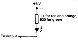
FIG. 16 a traffic light indicate circuit for use with the circuit
in Fig. 15 for demonstration purposes
The whole system is working near the upper limit of timing by means of CMOS gates; the leakage of the timing capacitors (which should be low leakage types such as tantalum beads} is becoming too significant. In a real-life traffic light, the electronic system would account for only a very small part of the cost. Maintenance costs are high, and a results of a failed traffic light chaotic, so high-reliability components (555 timers, at least) would be used.
But the exercise of designing logic systems is the same, and the designer must balance many different, and often conflicting, requirements to arrive at an optimum design.
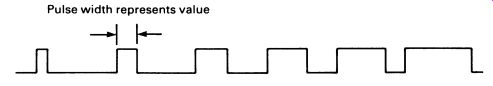
FIG. 17 pulse-width modulation ----- Pulse width represents value
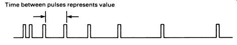
FIG. 18 pulse-position modulation ------ Time between pulses represents
value
3. PULSE-WIDTH MODULATION AND PULSE-POSITION MODULATION
Timing circuits can be used to encode information, either for transmission down wires or fiber-optic systems, or for modulating radio frequency carriers. There are two possible ways of sending information. If extreme accuracy is needed, then a purely digital method can be used, sending a stream of numbers that represent instantaneous values (as in digital sound recording). This is relatively complex and expensive. Where less accuracy is called for, a method known as pulse-width modulation can be used.
Pulse-width modulation (PWM) works by transmitting a stream of pulses, the duration of each pulse corresponding to a varying quantity. The principle is demonstrated in Fig. 17, which shows a sequence of pulses representing an increasing value. The resolution of the system will depend upon how finely the timing of individual pulses can be timed at the transmitter and measured at the receiver. PWM techniques are often used for transmission of digital data from computers, a long pulse representing a 1 and a short pulse representing a 0. The resolution of such a system need only be sufficiently good to distinguish between two possible values! A modification of PWM is pulse-position modulation (PPM), which uses fixed-length pulses but varies the time between them to represent analog values. Fig. 18 illustrates a PPM sequence, again representing a steadily increasing value.
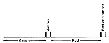
FIG. 19 the waveform for one complete cycle of the traffic lights:
pulse position modulation
With reference to the traffic-light timing system in Fig. 15, it should be clear how such pulses can be generated using digital circuits and timers. If the system does not need to respond quickly, relative to the pulse frequency used, both PWM and PPM can be multiplexed to provide information about several different variables. A counter in the transmitting system 'looks at' different variables in turn, and a similar counter in the receiver uses the interval between relevant pairs of pulses to recreate the original data. The traffic-light controller system of Fig. 15 actually produces a PPM signal which is applied to the clock input of the 4017. The 'events' that are represented by the spaces between the 250 JLS clock pulses are the times that each light is on. Fig. 19 shows the waveform for one complete cycle of the traffic lights, assuming that the 'green' is about 35 seconds and the 'red' is 40 seconds.
This train of pulses contains all the necessary information to operate traffic lights at some point remote from the timers. As with the television transmission, it is necessary to devise a system to synchronize the receiving counter with the transmitting counter; this might be a long pulse, a short burst of closely spaced pulses, or even a temporary cessation of the transmission. Synchronization is necessary to ensure that the multiplexing of the receiver is looking at the same channel as the transmitter.
Fig. 20 illustrates a PPM coded sequence for eight channels, with a long pause used to synchronize the transmission. The first four channels are showing a lower value than the last four. Each channel is 'updated' once every 20 ms or so, and it is not possible to change information at the receiving station more rapidly than this. The resolution of each channel is unaffected by the rate at which the signal is multiplexed, depending only on the accuracy of timing circuits in the transmitter and receiver.
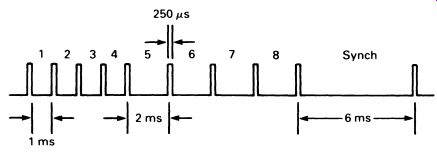
FIG. 20 pulse-position modulation for a multi-channel control transmission;
the long gap is used to synchronize the counters at the transmitter and
receiver
At the receiver, the signal can be decoded by a simple counter, with added circuitry for the synchronizing system. A suitable circuit is given in Fig. 21; this would decode the waveform of Fig. 20 into separate pulses.
The clocking signal is applied to the input of a 4017 counter, and also to the RESET input. RESET is normally held positive by the resistor, the capacitor being fully charged. When the input waveform goes negative, the capacitor is discharged through the diode and RESET goes low, allowing the counter to work. The time constant of the circuit is chosen so that RESET rises above half the supply voltage only during the 6 ms synchronizing pulse.
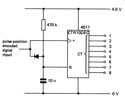
FIG. 21 a pulse-position decoder circuit, suitable for use with
the encoder circuit in Fig. 22.
During the gap in the pulse train used to synchronize the system, the capacitor discharges beyond the point where the potential on the RESET input rises above half the supply voltage, causing the counter to reset to zero. Note that the receiver will operate correctly with any number of channels, from one to ten, provided the synchronizing system is working.
If it appears that the principles of PPM transmission and reception have been given in greater detail than might be expected, then it is for a reason. The system described above is the standard method used for the radio control of models, and we can use the principles explained in this section, in conjunction with the transmitter and receiver circuits described earlier, to produce a working model control transmit/receive system.
The circuit in Fig. 22 represents the complete encoding and modulation system for the transmitter illustrated in Figure 15.3 and 15.13. In essence it is clearly very similar to the traffic-light controller in Fig. 15, and the principles of operation are much the same. A second gate (G3 ) inverts the output, and a single pnp transistor is used to increase the output current capability (a transistor used in this way is referred to as a 'buffer'). The circuit uses a 4022, an IC that is almost identical to the 4017, but counts up to eight instead of ten. The transmitter encoder provides seven identical independent channels of control. The synchronizing interval is generated by R5C5, providing a fixed pulse of about 6 ms. All the other channels are variable between 1 and 2 ms, the standard values that represent 'full left' and 'full right' to a model control servo (see below). In the center position, the pulse interval is 1. 5 ms ('straight ahead'). Supply decoupling (see Section 10) is provided by the 2200 resistor and the 10 uF capacitor, which prevent transients on the power-supply lines from triggering the 4022 spuriously.
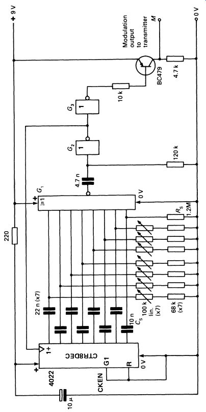
FIG. 22 complete coding system for an 8-channel radio control; the
output of this circuit can be used to modulate the transmitter described
in Section 15.
The radio control receiver decoder works on this principle, the input to the decoder being driven by the receiver's output. CMOS circuits are relatively unaffected by voltage fluctuations resulting from heavy loads imposed on the battery by servos. Not so the receiver circuits. In order to hold the supply voltage to the receiver constant, decoupling is required in the power line between the decoder and the receiver. A simple decoupling circuit (Figure 10.12) is not effective enough, so a transistor is used to improve the performance. This circuit is similar to the simple regulator circuit shown in Figure 10.26, but with a capacitor replacing the Zener diode.
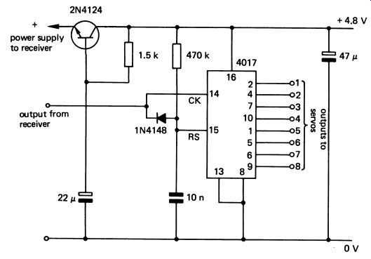
FIG. 23 the complete radio control receiver decoder, including a
voltage regulator for supplying the receiver. This circuit can be used
with the receiver described in Section
15 The decoder and de coupling
circuit is shown in Fig. 23. This circuit connects directly to the
circuit in Figure 15.23 to make
the complete radio control receiver.
Model radio control servos are best obtained ready-made, as the mechanical parts are small and have to be precise. The electronics in the servo convert the 1-2ms pulse into a mechanical movement, the system diagram being given in Fig. 24.
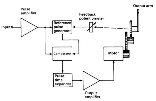
FIG. 24 system diagram for a typical model control servo
A specially designed IC is used, the NE544. This, along with a few discrete components, a motor, gears and feedback potentiometer, are all squeezed into a plastic case about 40 x 30 x 20 mm! Model servos are designed to be used with multi-channel systems, and accept an input pulse supplied at the rate of one every 20ms or so. Most servos require a 'positive pulse', which is the type used for the receiver described in this guide.
Servos can be tested with a circuit that provides the requisite pulses the circuit of Fig. 8 is ideal! The two outputs provide suitable pulses for either type of servo.
The operation of the servo is typical of a feedback control system, and works as follows. A small, high-efficiency motor is connected through a reduction gear system to the servo output arm, and also to a potentiometer. This potentiometer is connected to the reference pulse generator (see Fig. 24). Imagine the servo is in its 'center' position when a 1.5 ms pulse is received. After amplification the pulse is fed to the comparator. The incoming pulse also triggers the reference pulse generator, which, while the potentiometer is in the middle of its travel, is also 1.5 ms long. While the pulses are the same length, there is no output from the comparator.
If the incoming signal is now reduced to 1 ms (command for 'full left'), the comparator detects a difference between the incoming pulse and the reference pulse-the incoming pulse is 0.5 ms shorter. This causes an out put from the comparator, which, via the pulse time expander and output amplifier, drives the motor. The motor rotates both the output arm and the control potentiometer until the reference pulse is also 1 ms long and the output from the comparator ceases.
Increasing the input pulse length to 2 ms ('full right') again causes an output from the comparator, but because the incoming pulse is now longer than the reference pulse-by 1 ms-the output is of the opposite polarity. Once again, power is applied to the motor, but in the opposite sense so that the motor turns the other way. The output arm and potentiometer again turn until the reference pulse once again matches the input pulse.
Advantages of this system are (i) the servo uses little power unless it is changing position, (ii) the motor will work against any attempt to force the output arm into a different position, and (iii) a lot of torque is avail able, better than 2 kg/em for an average servo.
This section, dealing principally with digital circuits and timers, has actually brought together several aspects of electronics and electronic systems.
Timers have led to the design and development of a traffic-light con trol system. Digital transmission of data, based on timers, has led to a data-encoding and decoding system. And finally, the data system has been used to modulate a transmission that can be received by a receiver system (both transmitter and receiver having been described elsewhere in the book). The result is a practical system, fully compatible with current commercial model control systems, that can form the basis of an interesting project for students.
When using the radio-control system, be careful about safety. The 27 MHz band, used for model boats, cars and aircraft, is open to interference from CB radios working at 27 MHz on different but very close frequencies. Power model aircraft can be dangerous, and the 35 MHz FM band, also available in the UK for aircraft only, is preferable in this case.
In the next section, we shall examine systems that are 'pure' digital electronics, operating without the use of 'analogue' timers.
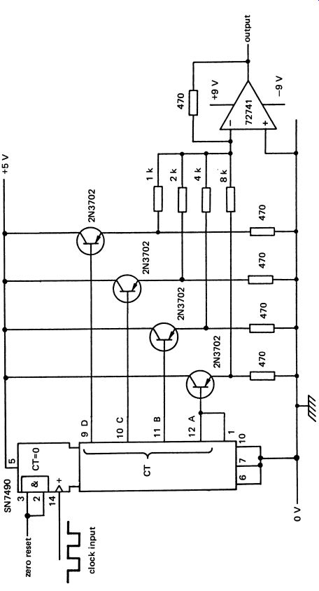
FIG. 25 a simple digital to analog converter, using a TTL counter
and
4. DIGITAL TO ANALOG CONVERSION
Although the circuits we have been considering have transmitted information by means of digital pulses, the information content has actually been in an analog form. The time between each pulse is a continuously variable quantity and is therefore analog in nature, and not digital.
However, it is often convenient to treat analog quantities (sounds, movement, heat, light) as numbers for the purpose of digital processing. A typical example is the digital recording system outlined at the beginning of Section 18. Before such a system can be developed, we need systems for converting digital information to analog values, and vice versa. Several techniques exist.
It is relatively easy to translate a binary number into a voltage. The circuit in Fig. 25 is typical. The SN7490 4-bit binary counter drives four 2N3702 pnp transistors, one for each bit, that are either cut off or fully on according to whether the bit is zero or one. A proportion of the emitter voltage of each transistor is applied to the inverting input of an SN72741 operational amplifier. The voltage from each transistor is proportional to the value of the bit, each successive higher bit applying twice the voltage of the previous bit. The op-amp sums the voltages, and the output is a voltage that is an exact analog of the binary number. For obvious reasons, this kind of digital to analog converter (abbreviated to DAC) is called a weighted resistor DAC. Fig. 26 shows the output for an increasing count.
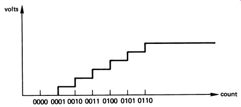
FIG. 26 the output of the converter in figure 22.25, as the count
increases To all intents and purposes the weighted resistor DAC operates
instantly.
The analog output follows the digital input without any delay other than those inherent in the semiconductor devices being used. The opposite kind of conversion, analog to digital (ADC) almost always takes time, and different circuits are used according to the design requirements.
5. ANALOG TO DIGITAL CONVERSION
The simplest kind of ADC is the single-slope conversion ADC. The system is shown in Fig. 27. The principle is quite easy to understand. The counter is reset and the voltage to be converted is applied to the inverting input of an op-amp. The non-inverting input is held at zero volts, as the output of the DAC (the circuit in Fig. 25) is zero because the count is zero. The output of the op-amp is therefore positive. This applies a 1 to the AND gate. The clock generator puts a square-wave on the other input of the AND gate, and the output of the AND gate turns on and off with the clock waveform. This makes the counter count up, and the out put from the DAC rises in a series of steps. There comes a point when the output voltage from the DAC exceeds the input voltage being measured.
When this happens the output of the op-amp swings from positive to negative, applying a logic 0 to the AND gate and cutting off the clock signal to the counter. The count stops increasing, and the digital equivalent of the input signal can now be read on the digital output lines of the DAC. The state of the output of the op-amp is used to indicate when the digital output is ready to be read. Once the value has been read by other circuits--and perhaps latched into a display--a pulse can be applied to the RESET input of the counter. The cycle then repeats.
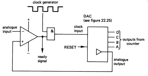
FIG. 27 schematic diagram of a single-slope conversion ADC It is
clear that although it will provide a continual digital conversion, this
kind of circuit takes a little while to operate. The length of time taken
for a 'reading' is actually proportional to the voltage being converted
and the speed of the clock. If the circuit is intended to provide a conversion
that follows, or tracks, the input voltage, then it can be modified to
improve the performance. The tracking ADC (or servo-type ADC) uses a
similar principle except that the counter is an IC designed to count
up or down. It is connected in such a way that it counts up if the op-amp
used as a comparator shows that the input voltage is higher than the
last value, and down if it is lower. This increases the speed of each
conversion as the counter only has to count up or down by an amount corresponding
to the difference between the current input voltage and the last one.
Fig. 28 illustrates a different type of single-slope ADC. A capacitor is charged up at a known rate from a known voltage source, so it is possible to predict exactly what voltage it will have reached after a set time.
The input voltage (the voltage to be converted) is applied to one input of an op-amp, and the voltage across the capacitor is applied to the other. A stable clock-pulse is gated by the output of the op-amp. Conversion takes place as follows.
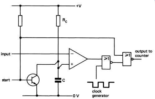
FIG. 28 schematic diagram of a single-slope conversion ADC, using
a different technique from the one employed in figure 27.
The capacitor, initially uncharged and holding zero volts on the op-amp's input, begins to charge up. Clock pulses appear at the output. When the voltage across the capacitor reaches a level where it just exceeds the input voltage, the output of the op-amp changes polarity, and the clock pulses no longer appear at the output. The number of clock pulses that have been delivered to the output since conversion started depend on the time taken before the voltage across the capacitor and the input voltage are equal.
Thus the number of clock pulses delivered to the output is proportional to the input voltage. The digital equivalent can be found simply by counting the pulses.
The above circuits all use single-slope conversion, in which a steadily increasing voltage is compared with the unknown input voltage. For many applications greater accuracy can be obtained using dual-slope conversion, shown in Fig. 29. The capacitor is charged up from the input for a fixed period, equal to the length of time it takes for the counter to reach its maximum count. When this happens, a 'carry' output from the counter disconnects the input and discharges the capacitor through a known resistance. The counter is incremented by the clock pulses until the capacitor has discharged, whereupon the counter shows the digital equivalent of the input voltage. A graph of the voltage across the capacitor shows a steady increase while it charges, then a steady decrease while it discharges – the 'dual-slope' in the name of the circuit. Dual-slope ADCs are slow, but are often used for meters because they are relatively immune to input voltage transients that can make faster systems give erratic results.
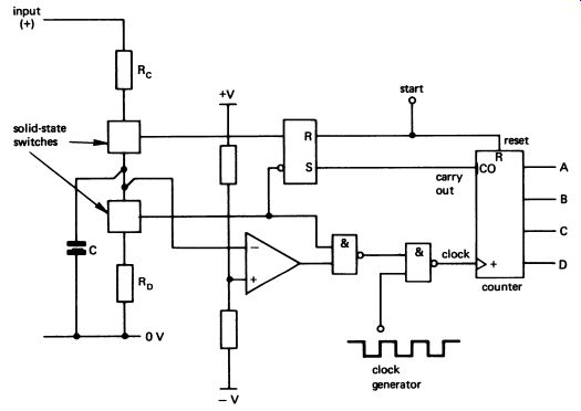
FIG. 29 schematic diagram for a dual-slope conversion ADC.
One of the fastest types of ADC is the successive approximation ADC. In this design, a voltage corresponding to the value of each bit is compared with the input voltage. The bit is then either set or not set, and, if set, the equivalent voltage is subtracted from the input voltage. This system is complicated, but requires only one clock cycle per bit to carry out the conversion.
The very fastest conversion, such as might be used for audio work, is carried out by using a separate op-amp for each bit, comparing the input voltage simultaneously with voltages that will result in a positive (1) or negative (0) output from the op-amps corresponding to each bit. This kind of circuit operates at a speed depending only on the slew rate of the op amps, and is called a clock less ADC All the different types of DAC and ADC are available in integrated circuit form, and there are many different designs, all slightly more suit able for one or other application.
QUESTIONS
1. Sketch a system diagram in which the output of a timer operating in astable mode is turned on or off by a logic gate.
2. Sketch the circuit diagrams for CMOS and TTL astable circuits.
3. Draw a graph showing the pulse sequence 0111001 as a pulse-width modulated waveform.
4. Draw a graph showing a triangular waveform. Draw a graph of the same waveform, on the same time scale, as a pulse-width modulated transmission.
5. At what point on the excursion of the input from logic 0 to logic 1 does the output of a CMOS gate change state?