AMAZON multi-meters discounts AMAZON oscilloscope discounts
In the first sections of this guide we have used a model of the atom origin ally designed by Niels Bohr. It is easy to picture the Bohr atom, with its hard, bullet-like electrons hurtling round the massive nucleus just like planets orbiting a sun in a tiny solar system. The work done by Werner Heisenberg in the late 1920s showed that this model is unfortunately further from reality than we might find comfortable and that the atom is actually a rather fuzzy and uncertain thing, not at all like Bohr's micro miniature solar system. This is not a guide about atomic physics, so it is unnecessary to look too closely at the construction of atoms-but it is important to realize that there are 'rules' that appear to govern the behavior of atoms and their component parts. Many of these rules seem contrary to what we would expect; but our intuition is necessarily based on our experience of the behavior of objects much larger than atoms and electrons.
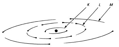
FIG. 1 one model of the silicon atom
Consider an individual atom of an element-silicon is a useful example.
The atom consists of a central nucleus surrounded by a cloud of electrons, which can be represented diagrammatically in FIG.1.
The electrons arrange themselves into three orbits, or 'shells'; although the diagram shows the electrons in a flat plane, the orbits actually occupy a spherical 'shell'. The shells are given letters, starting with K for the inner most shell, then L and M, and if there are more than three shells N, and so on. Each shell can hold a specific number of electrons, two in the K shell, eight in the L shell, and eighteen in the M shell. As we build up models of different atoms, the shells are filled from the orbit nearest the nucleus, so silicon (which has fourteen electrons) has full K and L shells (two and eight) and the remaining four electrons in the M shell.
This seems straightforward enough, but if we look closer at the atom we find a little of Heisenberg's 'fuzziness' beginning to creep in. One of the rules governing the behavior of electrons in a system (a system means an atoms or group of atoms) states that no two electrons can be at precisely the same energy level.
What does 'energy level' mean in this context? Go back to the solar system analogy and imagine a spacecraft orbiting in the K shell. Run the engines to increase its speed, and it will move out to a more distant orbit, perhaps even as far as the L shell. Subtract energy from the spacecraft by allowing some energy to dissipate as heat (it's a low orbit, in the outermost fringes of the atmosphere, and is subject to a little drag!) and it will drop into a lower orbit. Thus it is clear that the greater the energy possessed by the spacecraft, the higher-further from the nucleus-will be its orbit.
If no two electrons can have the same energy, it follows that no two electrons can orbit at exactly the same distance from the nucleus. It also follows that the shells consist of more than one possible orbit. The L shell, with its eight electrons, must consist of at least eight different orbits, all close to one another but not the same. Can we say how these orbits are arranged, and which of the possible orbits are in fact occupied by an electron? Unfortunately we cannot. Another of the rules governing the behavior of electrons says that we cannot know the speed, position and direction of an electron all at once. We can never say for certain the whereabouts of the eight electrons that form the L shell at any particular instant; all we can do is say where there is the greatest probability of their being located. Compare part of the 'Bohr' orbit in FIG.2a with the 'Heisenberg' version in FIG.2b.
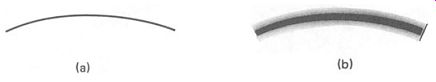
FIG. 2 two models showing sections of an electron's orbit
The degree of shading in FIG.2b represents the degree of probability of an electron being in that particular orbit. This is all we can say about the electrons, not because of any limitations in our measuring equipment, but because of the very nature of electrons. This rather odd fact about electrons is one of the more important discoveries to come out of modern quantum physics.
But Bohr's model is reliable in that there are specific regions (or shells) that the electron can occupy. It is not possible for electrons to orbit between the shells. We can redraw FIG.1 to show the probabilities of electrons being in any particular orbits (see FIG.3).
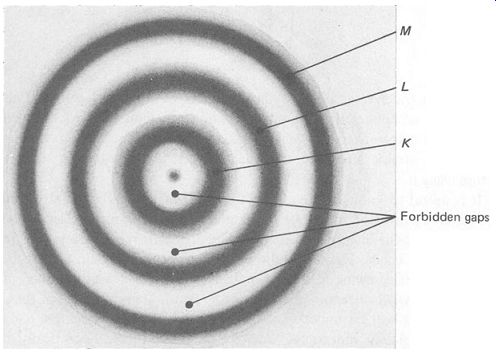
FIG. 3 atomic model showing energy bands and forbidden gaps
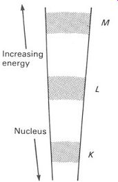
FIG. 4 a section of the orbits shown in FIG.3
It now seems more realistic to call the shells 'energy bands', as they represent a range of possible electron energies. The higher the energy, the further it will be from the nucleus. Electrons may not orbit in the for bidden gaps between the shells. The outer band is called the valence band and is the only band that may not be completely full.
If we take a section through this model of the atom, from the nucleus to the outermost band, we can represent this by a diagram showing just a small part of each orbit-like the one in FIG.4. We can use this as an energy-level diagram for our atom, since the bands represent electrons having increasing energy as we go up the diagram. The degree of 'fuzziness' of the bands depends on the temperature, and it is normal to show energy level diagrams for a temperature at (or very near) absolute zero.
It is possible to make an imaginative jump and use one energy diagram to represent the average of a very large number of atoms in a system. This is what we do to describe the operation of semiconductor devices. Such energy-level diagrams are, as we shall see, very useful aids to understanding quite subtle atomic interactions. But let us refine the diagram a little more before using it .. . . It is useful to know, for example, that the inner shells of the atom are not generally involved in any of the interactions that occur in electronics.
This simplifies the energy-level diagram, for it means we can simply leave out the lower bands. FIG. 5 shows an energy-level diagram for a piece of silicon--just showing the valence band. There is a vast number of possible orbits-all different-making up the band. Many or most of these possible orbits will be unoccupied. It is even possible to imagine a band which is completely unoccupied! Such a band is still there, theoretically at least, as it defines the probable positions of any electrons that somehow gain so much energy that they leave the valence band. So it is useful to add another band to the energy-level diagram, an 'empty' band beyond the valence band. This band is called the conduction band, and both it and the valence band are shown in FIG. 6.
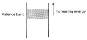
FIG. 5 possible orbits in the valence band

FIG. 6 energy-level diagram showing the valence and conduction bands
(the conduction band need not have any electrons in it)
1. CONDUCTORS AND INSULATORS
We can use energy-level diagrams to explain why conductors conduct and insulators do not. Compare the energy-level diagrams for copper and sulphur (FIG.7). In FIG.7a there is no forbidden gap between the valence and conduction bands. Electrons can move freely from band to band and there is no barrier to electron movement-a small increase in energy can move an electron into the conduction band. Once in the conduction band, the electrons are not bound to the structure of the atoms, and are free to drift through the material as an electric current.
Sulphur is different. The sulphur atom has a rather large forbidden gap between the valence and conduction bands. A moderate increase in energy will not be sufficient to move an electron out into the conduction band, but would only lift the electron as far as the forbidden gap. Since electrons cannot exist in the forbidden gap, they will not be able to accept such an energy increment, and will stay in the valence band. The conduction band will remain empty, and no current can flow.
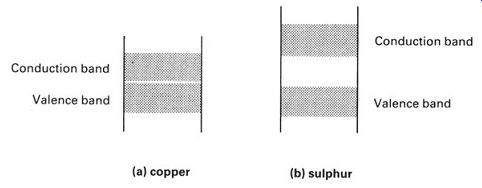
FIG. 7 energy-level diagrams of a typical conductor (copper) and
a typical insulator (sulphur)
2. INTRINSIC SEMICONDUCTORS
FIG.8 shows an energy-level diagram for germanium. The forbidden gap between the valence and conduction bands is very small and it requires only a little added energy, such as the thermal energy available at normal room temperature, to cause a few electrons to jump into the conduction band. Germanium will therefore conduct electricity, but poorly-less than a thousandth as well as copper, in fact. Germanium is called an intrinsic semiconductor, since it naturally has properties between those of conductors and non-conductors. The conductivity of germanium is strongly affected by temperature, as you might expect. The higher the temperature, the more the energy bands blur and expand, and the smaller the forbidden gap becomes.
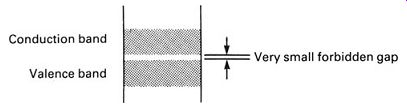
FIG. 8 energy-level diagram showing a typical intrinsic semiconductor
3. CHARGE CARRIERS IN SEMICONDUCTORS
We have seen how electrons can drift through a material in the conduction band and how this forms a flow of electric current. Electrons that are free to move about in this way are called charge carriers, because they carry electric charge through the material. But there is another mechanism by which charge can be carried through a substance, and we can see how this operates by looking at an energy-level diagram showing what happens when an electron makes the transition from the valence band to the conduction band (see FIG.9).
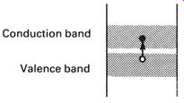
FIG. 9 when the electron moves from the valence and into the conduction
band it leaves a hole in the valence band
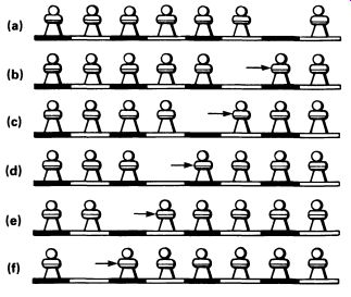
FIG. 10 the movement of electrons in one direction is the same as
movement of holes in the other direction; this can be demonstrated using
a chess board with a row of 7 pawns--( a) shows the initial arrangement:
one pawn is moving to the right in each stage of this diagram, (b) to
(f). Although no electron has moved more than one place, the hole has
drifted from the extreme right of the row to the extreme left
The movement of an electron from the valence to the conduction band provides a 'free' electron in the conduction band, but it also leaves a hole in the valence band, i.e. a gap into which an electron might easily move.
The hole could be filled by another electron in the valence band, but this would leave a hole somewhere else, which could be filled by another electron, leaving another hole in the valence band, and so on, and so on.
The creation of the electron-hole pair that results from an electron moving from the valence to the conduction band actually allows electrons to move about freely in the valence band as well as in the conduction band, though it is conventional to think of movement of electrons in the conduction band and of movement of holes in the valence band. FIG.10 shows clearly how a movement of holes is really the same as a movement of electrons in the opposite direction-both ways of looking at it are equally valid. Just as the electron carries one unit of negative charge, so the hole can be said to carry one unit of positive charge, which will in the right circumstances exactly cancel out the negative charge on the electron.
It is reasonable to ask at this stage just why we should bother to describe such a relatively complicated mechanism when the net result is simply an electron drift through the conduction and valence bands. The answer is that in the artificial semiconductors used in electronic devices we can deliberately introduce an excess of either holes or electrons into a sub stance, and it is often one or the other mechanism which dominates the conduction inside the material. Artificial semiconductors are known as extrinsic semiconductors.
4. EXTRINSIC SEMICONDUCTORS
We start with a cheap, plentiful semiconductor like silicon, purify it until it is absolutely pure, and then add a tiny amount of another substance- one part in 100 000 000 of phosphorus, for example. The resulting mixture is then made into a single perfect crystal. Because of its atomic structure, the phosphorus atom fits nicely into the crystalline matrix of the silicon, but with one electron left over in its outer shell, for it has five and not four electrons in its valence band. This extra electron is 'spare' to the structure of the crystal, and moves easily into the conduction band. An energy-level diagram for a crystal of silicon 'doped' with phosphorus is shown in FIG. 11. We show the extra electrons in the conduction band as minus signs. Such a doped semiconductor is called an n-type semi conductor, the n representing 'negative' to indicate that the material has extra (negatively charged) electrons.
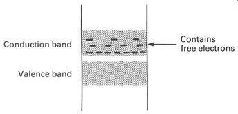
FIG. 11 energy-level diagram for an n-type semiconductor
Alternatively we could add to the silicon crystal matrix a few parts per million of boron. The boron atom has only three electrons in its valence band, and it too drops neatly into the silicon crystal structure. But it leaves a hole. This hole is easily filled by an electron from the valence band, leaving a corresponding hole in the valence band--and we have already seen that such holes act as positive charge carriers. Silicon doped with boron is therefore known as a P-type semiconductor, indicating that it has extra (positive) holes in its structure that can work as charge carriers.
A suitable energy-level diagram is given in FIG.12. Most of the holes appear at the top of the valence band, with their concentration falling off nearer to the nucleus. In FIG.11 the electrons had their highest concentration at the lower levels.
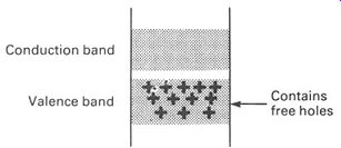
FIG. 12 energy-level diagram for a p-type semiconductor
This seems less strange when you realize that a hole needs more energy, not less, to get nearer the atomic nucleus. The concentration varies through out the band because there are more electrons (or holes) that just have enough energy to cross the forbidden gap. Progressively fewer have sufficient extra energy to take them deeper into the band.
For the purposes of describing semiconductor operation, it is a good idea to have an energy-level diagram that refers specifically to the electrons and holes. FIG. 13 looks the same as the energy-level diagrams we have used so far in this section, but ;we can use the shading to show the probability of finding electrons or holes (as charge carriers) in the bands. You will discover how useful this diagram can be for describing the way semi conductor devices work in the next section.
Before leaving FIG.13, let us be completely sure what it shows. It is an energy-level diagram for a piece of material as a whole. The upper band is the conduction band. It may be empty or it may have electrons in it. Any electrons in the conduction band can move freely through the material, and each electron carries one unit of negative electric charge. The density of the shading corresponds to the probability of finding free electrons at any given level in the band.
The space between the bands is the forbidden gap. No electrons can exist with this energy level, though they can cross the gap (apparently in zero time, although that's another story ... ).
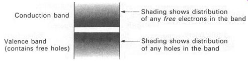
FIG. 13 an energy-level diagram illustrating distribution of holes
and electrons (this diagram will be used extensively in Section 7)
The lower band is the valence band. Its electrons are usually locked into the atomic structure, but in semiconductors there may be holes in it. Holes can drift about freely in the valence band, and are each carriers of one unit of positive electric charge. The density of the shading represents the probability of finding holes at any given level in the valence band.
We do not consider the absolute values of the energy levels, any more than we consider the inner bands of the atomic structure, for they are not relevant to the way semiconductor devices work. The energy is actually the total kinetic and potential energy of the electrons, and is a function of the physical structure of the material and also of any applied electrical potential. If an electric charge is applied to the material, the width and relative position of the energy bands will be unaltered, but the total energy in the system will change, moving the whole system of bands up and down the energy scale. Thus a negative electric potential applied to a material will move all the bands of the diagram up the energy scale, by adding to the energy (negative) of all the electrons.
An applied positive charge will move all the bands down the diagram.
You will see this overall movement of energy bands in the next section, where we will be looking at the simplest of common semiconductor devices, the pn diode.
5. MANUFACTURE OF SEMICONDUCTORS
It is harder than you might think to manufacture a piece of n-type or p-type silicon. The first step is to purify the silicon, using the best chemical techniques available. 'Chemically pure' silicon may contain an almost negligible amount of impurity, but this is enough to make it quite useless for making semiconductor devices. Silicon in which the impurities are measured in parts per billion is needed. A technique known as zone refining was developed. Zone refining consists of taking an ingot of pure silicon, and repeatedly moving it through a radio-frequency heating coil in the same direction. FIG.14 illustrates this. The heated area sweeps all the impurities down to the end of the ingot, until eventually, after many passes through the coil, the major part of the bar is pure enough.
The end of the ingot is cut off and sent back for chemical purification again.
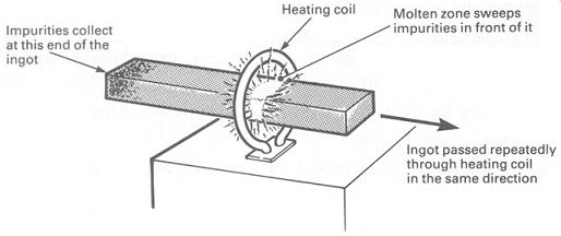
FIG. 14 zone refining a silicon ingot; the ingot is passed repeatedly
through the heating coil, which sweeps all the impurities down to one
end of the ingot
Next, the silicon must be made into a crystal. Most solids, when they are cooled from a molten state, crystallize into many individual crystals, with distinct boundaries between each crystal. This is not good enough for semiconductor devices--a single, large crystal is needed. The silicon is heated to a fraction above its melting point in an inert container (that is, a container made of a material like quartz, which will not react with the silicon). A single tiny silicon crystal is dipped into the molten silicon, and then withdrawn very slowly; the molten silicon makes the crystal 'grow', and if conditions are exactly right a sausage-shaped single crystal, about 50 mm diameter, can be drawn out.
The impurities required to make p-type or n-type silicon must also be added. There are two possible ways in which this can be done. Most obvious, the required impurities can be mixed into the molten silicon before the crystal is drawn. This method is often used. A second method, less obvious but potentially much more useful, is to add the impurities by a process known as diffusion. If the crystal 'sausage' is cut into thin slices-known in the trade as wafers--the required dopants (controlled impurities) can be added to each wafer as required. The wafer is first heated to about 1200°C (lower than the melting point of silicon) and then exposed to an atmosphere containing, for example, phosphorus.
The phosphorus atoms diffuse into the silicon, and change it into n-type silicon. The usefulness of the process is that it is possible to control quite accurately the depth to which the phosphorus diffuses. This is important in making most modern semiconductor components.
The same process can be used to make p-type silicon, simply by replacing the atmosphere of phosphorus with one of boron.
It is even possible to add an insulating and protective layer of silicon dioxide by putting the wafer into an atmosphere of water vapor and oxygen at a high temperature. The diffusion process makes many things possible and is crucial to the manufacture of devices from diodes to integrated circuits, as we shall see in the next few sections.
QUESTIONS
1. If an electron's energy is increased, what will happen to its orbit round the atom's nucleus?
2. Only one energy band in a atom may not be completely full. Which?
3. A conductor can carry an electric current, whereas an insulator will not. At an atomic level, what is the crucial difference between conductors and insulators?
4. Describe briefly the process used to make n-type silicon for use in transistor manufacture.
5. Explain (i) extrinsic semiconductor, (ii) forbidden gap, (iii) holes, in the context of semiconductors.