AMAZON multi-meters discounts AMAZON oscilloscope discounts
The special properties of semiconductors are utilized to make a wide variety of electronic components, ranging from diodes to microprocessors.
A detailed understanding of one of the simplest semiconductor devices, the pn junction diode, is an important prelude to a study of more complicated devices, and it is here that we begin.
A diode is basically the electrical equivalent of a one-way valve. It normally allows electric current to flow through it in one direction only.
The symbol for the diode is given in Figure 1.
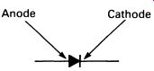
FIG. 1 circuit symbol for a diode
The arrowhead in the diagram shows the permitted direction of conventional current flow (remember, electron current goes the other way). Diodes can be made to handle currents varying from microamps to hundreds of amps-a selection of types is shown in Figure 2.
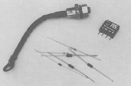
FIG. 2 a selection of diodes of various power ratings, from 1 A to
20 A
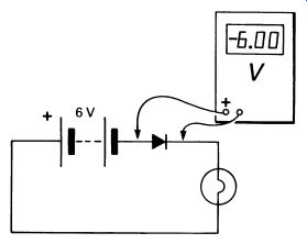
FIG. 3 a circuit to reverse-bias a diode; note the meter is connected
with its '+' to the battery '-', which results in a negative reading
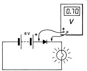
FIG. 4 a circuit to forward-bias a diode: the forward current is
limited by the lamp
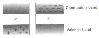
FIG. 5 energy levels for two separate pieces of semiconductor
A 'perfect' diode would probably have infinite resistance in one direction, the 'reverse' direction, and zero resistance in the forward direction. A real diode exhibits rather different characteristics, the most notable of which is a forward voltage drop, which is constant regardless (almost) of the current being passed by the diode. Compare Figures 3 and 4. In Figure 7 3 the diode is reverse-biased and does not conduct. The lamp remains out and the meter shows the whole battery voltage appearing across the diode. In Figure 4 the diode is forward-biased, the lamp lights, and the meter shows 0.7 V across the diode. By using bulbs of different wattages to pass different currents through the circuit we can show that the 0.7 V is constant. The diode used in this demonstration is a silicon diode. If we were to replace it with one using a germanium semiconductor, the forward voltage drop would be constant at 0.3 V. What causes the voltage drop? To find out we must look at the way the diode functions at an atomic level, and go back to the energy-level diagrams.
Figure 5 shows an energy-level diagram for a piece of p -type silicon and a piece of n -type silicon; the two materials are not in contact.
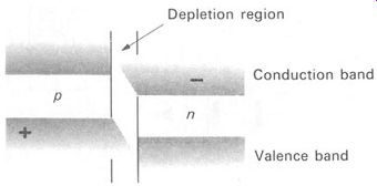
FIG. 6 energy levels for two pieces of semiconductor, one p-type
and one n-type, in contact with each other
Now we place the two pieces of silicon in intimate contact (fuse them together for best results) and the energy -level diagram looks like Figure 6.
A few moments thought will show what has happened. The p-type material has extra holes and then-type material has extra electrons. When the two types of semiconductor are put in contact the 'extra' electrons in the n-type material flow across the junction to fill up the holes in the p-type material. The electrons drift from then-type to the p-type through the conduction band, and then fall down into the valence band of the p-type material to annihilate one hole for each electron. The holes also move, drifting from the p -type to then -type semiconductor in the valence band.
Eventually an equilibrium is reached-but then-type material has lost electrons to the p-type, and lost energy in the process. The p -type, on the other hand, has gained energy and the result is the state of affairs represented by Figure 6. The 'hill' in the diagram represents an area in the junction between the two semiconductor materials about 0.5 um wide, called the depletion region, or sometimes the transition region. In this region there are no holes or free electrons. The 'height' of the hill, i.e. the difference in energy levels, can be measured in volts: for silicon it is 0.7 V, and for germanium it is 0.3 V. The junction between the p-type and n-type semiconductor is, in fact, the active part of the pn diode. A typical low-power pn junction diode might be constructed as shown in Figure 7.
Details of the way the diode is manufactured can be found in Section 11 , but for the time being it is enough to regard the diode as a block of p -type semiconductor in contact with a block of n- type semiconductor.
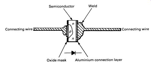
FIG. 7 construction of a low-power diode (the circuit symbol underneath
indicates the direction of current flow)
1. REVERSE-BIASING THE pn DIODE
Assume the diode is connected as in Figure 3, so that it is reversed-biased (non-conducting). The energy-level diagram for this state is shown in Figure 8.
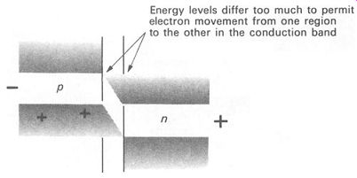
FIG. 8 energy levels in the reverse-biased diode
The energy of the p-type material is increased by the negative battery potential, while that of then-type is decreased. Look at the thickness of the conduction and valence bands and at their relative positions in the two different materials, on either side of the depletion region. No parts of the conduction bands or the valence bands have the same energy levels.
Electrons cannot move from the p-type to then-type material through the conduction band because even the least energetic electrons have too much energy. Similarly, holes in the valence band of the n -type material all have too little energy to drift into the valence band of the p-type. The energy levels of the bands on either side of the depletion region are too different to allow either electrons or holes to move from one type of material to the other.
It follows that if electrons and holes are unable to cross the depletion region, there can be no current flow, for electric current is a movement of electrons (or holes) along a conductor.
2. FORWARD-BIASING THE pn DIODE
Let us reverse the situation, and connect the diode as in Figure 4, i.e. to forward-bias it. The energy-level diagram for this state is given in Figure 9. This time, the battery potential decreases the energy of the p-type semiconductor, and increases the energy of then-type. When the potential applied is equal to or more than 0.7 V (assuming we are using a silicon diode and not a germanium one) the two types of material are at the same energy level, and the conduction and valence bands coincide. Both electrons and holes can move freely between the two types of semiconductor, and electric current can flow through the diode.
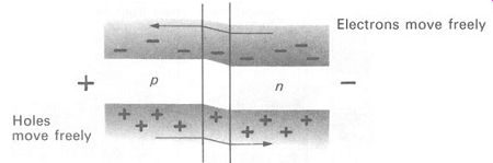
FIG. 9 energy levels in the forward-biased diode
The reason for the 0.7 V forward voltage drop of the silicon diode should now be clear. A potential of 0.7 V must be applied to the pn junction to equalize the energy levels, and this is effectively subtracted from the potential available to push electric current through the diode.
3. POWER DISSIPATION IN THE DIODE
It is the forward voltage drop that sets an upper limit on the amount of current we can get through a diode. The lamp in Figure 4 might use, for example, 1 A, and the battery might be 12 V. In such a case a current of about 1A flows in the circuit-but some of the power is 'wasted' in the diode as a result of the forward voltage drop, and is dissipated from the junction as heat. The amount of power that the diode dissipates can be calculated very simply using the formula:
P= V_r I
where P is the power (in watts), I is the current flowing (in amps), and Vr is the forward voltage drop of the diode in question. With 1 A flowing, the diode will dissipate 0.7 x 1 watts, or 0.7 W. When a diode is used in a circuit its power rating must exceed the expected dissipation, preferably by a comfortable margin.
In practice, the formula is complicated by the fact that the diode gets hot. The intrinsic conductivity of semiconductors increases with tempera ture (the bands get thicker) and this has the effect of lowering the forward voltage drop as the temperature rises. For both silicon and germanium the forward voltage drop decreases at the rate of about 2. 5 m vr c temperature rise.
Since the junction temperature of a silicon diode may exceed l00°C with the diode operating near its maximum current, temperature effects can become quite significant. The 'normal' forward voltage drop of0.7V is reduced to 0.45 V for a 100°C temperature rise. For most purposes this effect can be discounted, but in circuits where the voltage drop across the diode is important, we have to bear it in mind, it is not, incidentally, possible to reduce the forward voltage drop to zero-at very high temperatures, the junction melts. Silicon is much more tolerant of temperature than germanium. For this reason, and also because the reverse leakage current is much lower (see below), silicon diodes are the norm and germanium diodes are relatively rare-they are used only in applications where a low forward voltage drop is essential.
4. REVERSE LEAKAGE CURRENT
Diodes are 'imperfect' in another way. When connected in a circuit that reverse-biases it (Figure 3 again) a diode allows a very small current to flow. This current is called the reverse leakage current and is partly due to thermally generated electron-hole pairs and partly to leakage across the surface of the diode. The reverse leakage current is very small for silicon diodes, in the region of 2 to 20 nA. For almost all purposes this minute current can be ignored. The reverse leakage current for germanium diodes is much higher, typically 2 to 20 uA, and this may be important in some circuits.
The reverse leakage current is also temperature-dependent and for both silicon and germanium it roughly doubles for each 10°C rise in temperature.
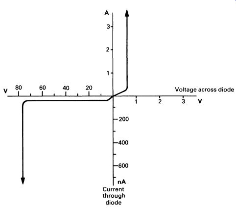
FIG. 10 conduction characteristics of a silicon pn junction diode
5. REVERSE BREAKDOWN
As the voltage applied to a diode to reverse-bias it is increased, there comes a point at which reverse breakdown occurs. In normal pn diodes, this breakdown is catastrophic and destroys the diode. Depending on the construction of the diode, the point at which reverse breakdown occurs can be anywhere from fifty to a few hundred volts. Manufacturers always specify the safe reverse-bias voltage, which is normally referred to as peak inverse voltage. Thus a 50 p.i. V diode can be reverse-biased at 50v without danger of breakdown taking place.
We are now in a position to draw a graph of a typical diode's conduction characteristics at room temperature (see Figure 10). Note that the four scales of the graph are different, to show different aspects of the characteristics. On the right, the voltage across the diode is shown for different values of current through the diode. The graph continues straight up until the current reaches a value that causes overheating (P = Vrl) and melts the pn junction. On the left, the reverse leakage current is shown for increasing voltage; it remains steady at a few nanoamps until reverse break down occurs (at a substantially higher voltage than the 50 p.i. V manufacturer's maximum for this device) and the current increases to a value limited by factors other than the characteristics of the pn junction, which at this point will have just ceased to exist.
6. THE ZENER DIODE
There is one particular type of diode that makes use of a form of reverse breakdown to provide a constant 'reference' voltage. The circuit of Figure 11 shows the symbol for a Zener diode and also a suitable circuit to demonstrate its properties.
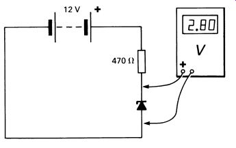
FIG. 11 a Zener diode in a typical circuit
In this circuit the diode is reverse-biased (Zener diodes are always used this way) and the meter shows a drop of 2.8 V across it. The voltage drop across a reverse-biased Zener diode will be substantially constant for all values of current up to the diode's limit, and for all values of voltage higher than the Zener voltage. A resistor is necessary to limit the current through the circuit; in this case the current is calculated by Ohm's Law:
12 - 2· 8 = 19.6 mA 470
If we were to double the battery voltage to 24 V, the current through the circuit would increase to 24-2.8 = 45mA 470
but the voltage across the Zener diode would remain at 2.8 V. The Zener diode is therefore a valuable device for voltage regulation, giving a fixed reference voltage over a range of input voltages.
Zener diodes are named after C. M. Zener, who in 1934 described the breakdown mechanism involved. In fact, Zener's description applies only to diodes with a Zener voltage of less than about 3 V. Above this, a mechanism called avalanche breakdown begins to take over. However, both types are generally lumped together under the heading 'Zener diodes', and are available in a range of voltages from 2 to 70, and with power ratings from 500 mW to 5 W. The power dissipation of the Zener diode is calculated by means of the usual formula
P= Vzl where Vz is the Zener voltage.
By way of example, the Zener diode in
Figure 11 is dissipating 2.8 x 19.6 = 54.9mW
The conduction characteristics of a Zener diode can be drawn in a diagram similar to Figure 10. Look at Figure 10 again- the only difference in the Zener diode's characteristic is in the reverse breakdown (lower left quadrant), which will occur at the Zener voltage. The important factor not shown in the diagram of characteristics-is that the Zener diode is undamaged by reverse breakdown provided that the current through the diode, and thus its heat dissipation, is limited to a safe value.
7. THE VARICAP DIODE
When a diode is reverse-biased, the junction behaves like a capacitor. The p-type and n -type regions form the plates of the capacitor, and the depletion region acts as a dielectric. You will remember that the capacitance of a capacitor depends on the thickness of the dielectric, and it is this fact that makes the pn diode useful as a variable capacitor. If the voltage used to reverse-bias the diode is increased, the difference in the energy-levels of the p and n regions is made greater. As this happens, more of the junction thickness is depleted of charge carriers, increasing the width of the depletion regions. Effectively, the capacitor's dielectric has become thicker, reducing the capacitance.
A varicap diode is a diode in which the change of capacitance with applied reverse voltage is enhanced as far as possible by the diode's physical construction. Even so, both the overall capacitance and the amount of change are fairly small, though they are sufficient to enable the varicap diode to be used in the tuning circuits of televisions, for example. A typical varicap application circuit is shown in Figure 12.
A tuned resonant circuit (see Section 15) is formed by L1 and C1 , VC1 (L 1 is made variable for initial adjustments) and a variable voltage applied via R1 • If this control voltage ( Vc) is changed, the capacitance of the vari cap diode is altered, varying the resonant frequency of the tuned circuit.
The control voltage could come from a TV channel-changing system, probably based on digital electronic techniques, and the resonant circuit could be used in the TV tuner.
Typical varicap diodes have a capacitance swing from 6 pF to 20 pF, for an applied reverse voltage of 2 to 20 V.
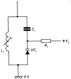
FIG. 12 a varactor tuning circuit, such as might be used in the tuner
of a television; changing the voltage at + V c changes the capacitance
of the varicap diode and alters the resonant frequency of the circuit
8. THE LIGHT-EMITTING DIODE
The light-emitting diode (LED) is an extremely useful device, and replaces miniature incandescent lamps in a whole range of applications. Almost everybody is familiar with the LED display, used commonly for digital alarm clocks. LED displays are usually ruby red, but green and yellow is also available (although more expensive and therefore less common). Figure 13 shows two different types of LED. Like ordinary pn diodes, LEDs have no inherent current limiting characteristics, and must be used with a resistor to limit the current flowing-generally to around 20 mA for a small LED indicator. A suitable circuit is shown in Figure 14. It is clear from the circuit that LEDs are used in the forward-biased mode: indeed, they must be protected from reverse-bias as they usually have a reverse breakdown voltage of only a few volts. If breakdown occurs, the LED is destroyed. LED displays are described in rather more detail in Section 16.
Mechanism of light emission
To move an electron from the valence band into the conduction band requires energy; and example of this is the creation of an electron-hole pair. Similarly, if an electron falls down from the conduction band to annihilate a hole in the valence band, energy is given off. In normal pn diodes, this energy takes the form, ultimately, of heat. In the LED, part of the energy is given off as light, the wavelength (color) of the light depending on the distance the electron falls, which in turn depends on the width of the forbidden band. LEDs are made with a variety of rather exotic materials: gallium arsenide phosphide for red or yellow, gallium phosphide for green.
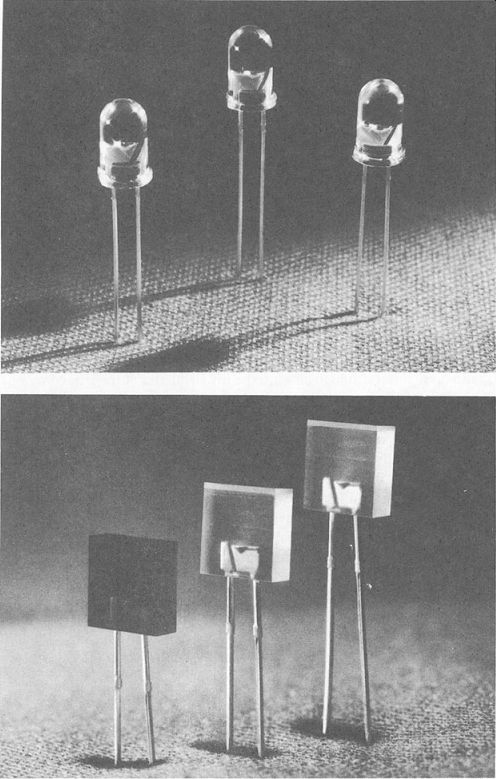
FIG. 13 some typical-light-emitting diodes (optoelectronics is discussed
in more detail in Section 16) ----- photographs by courtesy of Hewlett-Packard
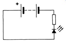
FIG. 14 a typical circuit for driving a LED; the resistor is necessary
to limit the current through the LED, which is used in the forward biased
mode
The physical design of a LED is important. Because the semiconductor material is rather opaque, most of the light produced never reaches the surface. To improve matters, the junction has to be very close to the surface, only about 1 ,.un or so. This means that the p or n region has to be very thin. Electrical connections to this layer have to be made in such a way that they do not obstruct the light. Figure 15 shows a typical LED. In practical applications LEDs are often pulsed. This is because the light output increases quite rapidly with increasing current, so a LED that is pulsed at 50mA (and is on half the time) will look brighter than it would with a continuous 25 mA, while dissipating the same amount of heat. The pulse repetition frequency has to be rapid enough for persistence of vision to make it look as if the LED is on continuously-more than about 50 Hz.
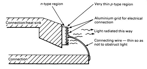
FIG. 15 physical construction of a LED; light is emitted through
the very thin p-type region and the device must be designed so that this
light is obstructed as little as possible; a large connection area is
made to the n-type region and this also serves to conduct heat away from
the junction like a pn diode, the LED exhibits a forward voltage drop.
This varies according to the type and color of the LED but is generally
between 2 and 3 V.
QUESTIONS
1. What is the value for the forward voltage drop of (i) a silicon diode, (ii) a germanium diode?
2. If a silicon diode is passing 2A, what is the amount of power that is likely to be dissipated by the diode?
3. How is the forward voltage drop of a diode affected by variations in temperature?
4. What is the main use of a Zener diode?
5. Which characteristic of semiconductor diodes is emphasized in varicap diodes?
6. A LED cannot be connected directly to a battery. What additional component is required, and why?