AMAZON multi-meters discounts AMAZON oscilloscope discounts
The transistor is perhaps the most fundamental device in modern electronics. It was the invention of the transistor that started the 'electronics revolution', and the transistor is still the most basic of all elements in an electronic circuit.
Various types of transistor are available, but there are two main classes: bipolar transistors and field-effect transistors. The first group is the subject of this section (the second is the subject of Section 9}. The circuit symbol for a typical bipolar transistor is given in FIG. 1.
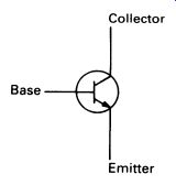
FIG. 1 circuit symbol for a transistor, npn type
The device has three terminals, referred to as the emitter, collector and base. Readers who are going through this guide in sequence and have read Section 5 will already be familiar with the thermionic triode valve, and will recognize a correspondence between the three terminals of the transistor and the cathode, anode, and grid of the valve. In many ways the transistor could be said to have 'replaced' the valve, for it is the same sort of device and is used to amplify electrical signals. But the similarity is not total. Whereas the valve responds to changes of voltage on the grid, the transistor is a current operated device, and provides an output current that is proportional to the input current. It behaves as if it were a variable resistor, the value of which depends on the current flowing through the base connection. Indeed, the name 'transistor' is a contraction of 'transfer resistor', which goes some way to describing the properties of the device.
The circuit in FIG. 2a shows a transistor in a test circuit configuration (but don't try it!), referred to as common emitter mode. If the input terminal A is made positive with respect to the emitter, a current will flow between the base and emitter. The base-emitter junction will behave exactly like a forward-biased semiconductor diode (see FIG. 2b).
FIG. 2 a simple transistor amplifier and an indication of the base
circuit
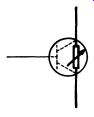
FIG. 3 the transistor places a variable amount of resistance in the
collector circuit
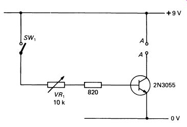
FIG. 4 a practical circuit for approximate measurement of transistor
gain
Within a certain range of base currents, the collector-emitter junction will exhibit the characteristics of a variable resistor, the resistance of which is inversely proportional to the base current (see FIG. 3). The output current of the transistor, measured on a meter in series with the collector, is larger than the input current by a fairly large constant, typically 20 to 1000, depending on the specific device.
A practical circuit for measuring a transistor's output current for a range of input currents is given in FIG. 4. Adjustment of the variable resistor VR 1 permits control of the base current, and makes it possible to check the output current for a range of input currents. The circuit is used as follows; with SW1 open, and VR 1 set to a maximum resistance, the meter is connected across the terminals of SW1 to read the base current.
VR 1 is set to give the required value of base current. The meter can now be removed and connected in series with the collector circuit, across terminals A-A. If SW1 is now closed, the collector current can be measured.
The advantage of this test circuit is that only one multimeter is required; the disadvantage is that there is no compensation for the resistance of the meter, which may affect the accuracy of the experiment. If required, a resistor equal in value to the resistance of the multimeter at the current range selected may be wired in series with SW1 for more accurate results.
Using the components specified in FIG. 4, the test can be performed for values of collector current up to about 200 mA. The battery may begin to flag at currents in excess of this, and if the collector circuit is left connected for any length of time, the transistor will get quite warm-after all, at 200mA (and once again assuming that the test meter has negligible resistance) it will be dissipating P= Vxl watts P = 9 X 200/1000 P= 1.8 watts For this reason, the specified transistor (an extremely high-power type) should be used in this circuit. Resistor R limits the base current to a safe value.
Over the range of collector currents from 10 to 200 mA, the calculation Ic/Ib (collector current/base current) should yield a value that is approximately constant. This constant is the large-signal current gain of the transistor when used in the common emitter mode (it can be used in other modes-more about them later in this section). This value is referred to by the symbol hFE. The hFE of the 2N3055 is quoted (by a manufacturer) as being between 20 and 70; there is quite a wide variation between different examples of the same device.
1. THE TRANSISTOR AMPLIFIER
It should now be clear how the transistor works as an amplifier. FIG. 5 shows a transistor amplifier circuit at its simplest.
A voltage applied to the input will cause a base current to flow, and the base current will be reflected in a change in collector current-which in turn will alter the voltage appearing at the output. A convenient way of visualizing this is to think of the transistor's collector circuit and the collector load resistor RL as forming two halves of a potentiometer, with the lower half variable in value as the base current changes. FIG. 6 illustrates this.
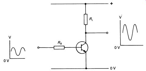
FIG. 5 a simple transistor amplifier, unlikely to be used in practice
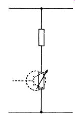
FIG. 6 the amplifier's output circuit as a potential divider
2. TRANSISTOR PHYSICS
Having briefly examined a typical bipolar transistor, we now turn to the physics of the device, and to the way it is constructed. A typical transistor is shown in FIG. 7. It is a three-layer device, and is similar to a pn diode in general appearance, except that it has an extra layer-compare FIG. 7 with Figure 7.7 (p. 84). An important piece of information-you will see why it is important as the description of the way the transistor operates progresses-is that then-type material is more heavily doped than the p-type material. The result of this is that the number of free electrons in the n- type semiconductor greatly exceeds the number of holes in the p type semiconductor.
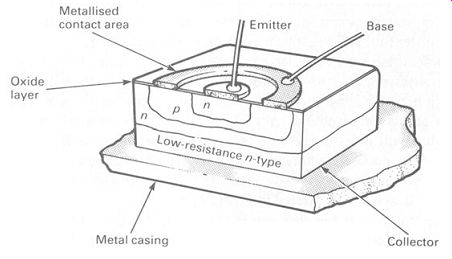
FIG. 7 physical construction of a silicon npn transistor
We can draw an energy-level diagram for the transistor, first when the device is 'at rest' with no power supply connected to any of the terminals.
FIG. 8 shows this.
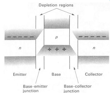
FIG. 8 energy-level diagram for the transistor with no voltage applied
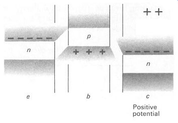
FIG. 9 energy-level diagram when the collector is positive relative
to the emitter fig 8.10 energy-level diagram when the base is more positive
than the emitter
Neither electrons nor holes can cross the depletion regions, because of the large difference in energy levels. If we now make the collector positive with respect to the emitter, as in the circuit shown in FIG. 5, the picture is different, changing to that shown in FIG. 9. Clearly, however, there is still no flow of electrons or holes through either junction.
When the base is made rather more positive than the emitter, the state of affairs changes dramatically, as illustrated by FIG. 10, in which a positive voltage is applied to the base to make it positive with respect to the emitter (but still negative in relation to the collector). Under these conditions, large numbers of electrons are able to flow from the emitter region into the base region, the energy levels at the emitter base junction having been made sufficiently close to allow electrons to move across the junction. A fairly small proportion of these electrons combine with holes in the base region. Restoration of the holes in the p type semiconductor requires a flow of electrons out of the base region (or a flow of holes into the base region). This constitutes the base current through the circuit illustrated in FIG. 2b.
The majority of the electrons in the base region drift towards the base collector junction, where the positive potential attracts them across the depletion region into the n -type material of the collector. Electrons can thus flow from the emitter to the collector, and this current flow constitutes the collector current, illustrated in FIG. 3.
The collector current is larger than the base current because the relative scarcity of holes in the lightly doped p -type base region limits the amount of current that can be drawn from the base by restricting the availability of charge carriers.
Because both electrons and holes are involved in its operation, this type of transistor is called bipolar, and because of its construction, with a p-type base region and n-type emitter and collector, it is called an npn transistor.
A few moments' thought will be enough to realize that it is equally possible to make a pnp transistor, having an n-type base and p-type emitter and collector. FIG. 11 shows the circuit symbol for a pnp transistor, in a circuit similar to the one in FIG. 5.
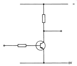
FIG. 11 a pnp transistor used in a simple amplifier circuit
Note that the polarity of the power supply is also reversed, with the base and collector at a negative potential relative to the emitter. Operation is the same as the npn transistor, but with the relative functions of holes and electrons exchanged.
Both npn and pnp transistors are readily available; npn types are some what more common, and generally a little cheaper.
Almost all modern transistors are made using silicon as the semiconducting material. Compared with germanium (see Section 6) silicon is less affected by temperature variations, and has fewer undesirable characteristics. There are a few germanium transistors available, and they can be used where a low forward voltage drop is essential.
3. BIPOLAR TRANSISTOR CHARACTERISTICS
The circuit configuration shown in Figures 5 and 11 is referred to as a common emitter circuit, the emitter being common to both input and output circuits. It is the most usual way of connecting a transistor. When used in this (or indeed, any other) mode, the transistor exhibits certain characteristics which we can use as a measure of its performance.
First, and perhaps most important, is the large signal current gain, the value we measured at the beginning of this section, expressed as the ratio Ic/Ib, collector current divided by base current, and given the symbol hFE· Unfortunately for those of us who like life to be simple, hFE is not constant, but varies with collector voltage. This is known as the Early effect (after the man who first suggested what caused it). One of the best ways of illustrating the way hFE changes with collector voltage is to plot a graph of collector current (/c) against collector voltage (Vee) for a range of different base currents (/b), choosing values for /b and Vee that are sensible for the transistor being measured. A typical set of graphs-called characteristic curves-is shown in FIG. 12, which is worth careful study.
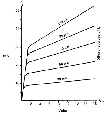
FIG. 12 transistor-characteristic curves
The straight, sloping part of the curve is called the linear region, and the transistor should be operated on this part of the curve for most purposes, for example for all types of linear amplifier. The almost vertical part of the curve marks the saturated region of the characteristics-the transistor 'switches' rapidly from a non-conducting to a conducting state (from 'off' to 'hard on') as the base current is increased. Transistors are operated in this part of the characteristic in digital circuits, where rapid switching and low power dissipation are important.
A feature of all transistors is leakage current, the current that flows into the collector when the base connection is disconnected (i.e. open-circuited). The base leakage current is given the symbol I ceo. For silicon transistors I ceo is very small, seldom as much as a few microamps. Germanium transistors have a much larger value of I ceo, often approaching a milliamp; in germanium transistors the leakage current is also intensely temperature dependent-so much so that they can be used as temperature-sensing devices. Silicon transistor leakage current is less affected by temperature at normal operating temperatures.
Temperature changes also affect the base-emitter junction voltage drop. For each 10°C rise in temperature the base-emitter voltage is reduced by about 20m V. Increasing temperature also changes the characteristic curves, spreading them out further apart and moving them upwards on the graph.
Finally, an increase in ambient temperature reduces the power-handling ability of a transistor by slowing the rate of heat transfer away from the casing (and thus the junction). Heat transfer from the transistor junction to the outside world is proportional to the temperature difference between them; a transistor's ability to dissipate heat is quoted in °C/W, being the temperature rise of the case (not the junction) per watt of dissipation at a given ambient temperature, usually 20°C. Heat radiators or heat sinks can be used to improve the heat-transfer capability by a substantial amount FIG. 13 shows some typical forms.
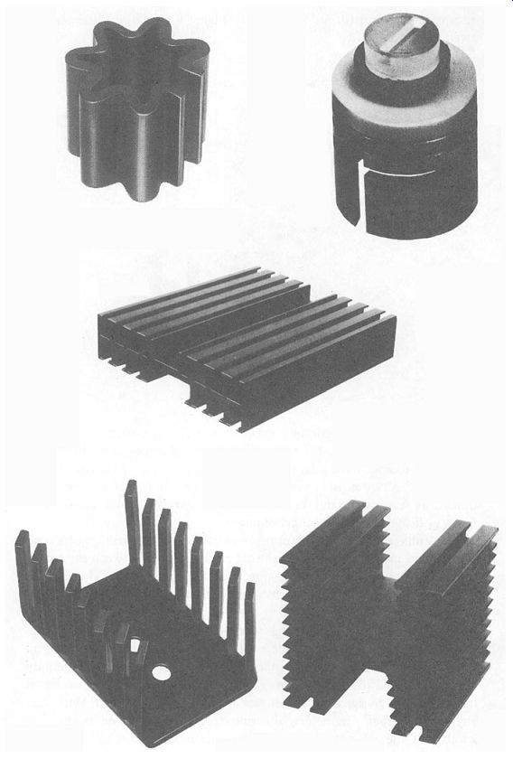
FIG. 13 a selection of heat radiators and heat sinks
4. SPECIFYING BIPOLAR TRANSISTORS
There are many thousands of different types of transistor, with every possible different specification. Manufacturers are continuously introducing new designs and withdrawing obsolete types. Broadly, there are 'design' types (the newest, for new equipment), 'stock' types and 'service' (obsolete) types. When a designer specifies a particular kind of transistor, the following main parameters are taken into account:
(1) Class. There are at least three classes of semiconducting device, according to its reliability, capacity for withstanding unpleasant environments--e.g. heat, damp, radiation-and physical construction. One large semiconductor manufacturer calls these classes 'military', 'industrial' and 'entertainments'. The best-military-components are substantially more expensive than the other two classes.
(2) Power. There are big transistors and small transistors. The big ones can dissipate as much as 150 W, whereas the smallest may overheat above 100m W. Transistors with large dissipations are called power transistors and are often designed so that they can be bolted to a suitable heat radiator.
The dissipation is partly a function of the size of the semiconductor chip, and partly a function of the arrangements inside the transistor for conducting heat away from the junction. A power transistor and a small plastic encapsulated transistor are compared in FIG. 14. Power dissipation is given the symbol PToT .
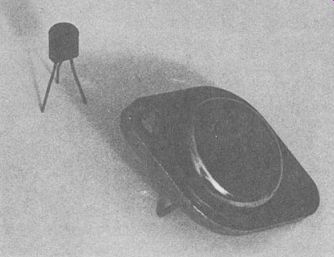
FIG. 14 comparison of large and small transistor encapsulations.
(3) Current. The maximum continuous collector current a transistor can pass is given the symbol Ic(MAX). It is related to power in that power transistors usually have a larger value of Ic(MAX) than small-sign transistors, but the power is of course a factor of current and voltage . Most transistors can withstand collector currents several times larger than Ic(MAX) if they are of very short duration.
(4) Voltage. The most useful measure of the working voltage of a transistor is the maximum safe voltage that can be applied between the collector and emitter when the base connection is open-circuited. This is given the symbol Vceo• and may be anywhere between ten and a few hundred volts.
(5) Gain. We have already dealt with hFE, the most convenient measure of a transistor's current gain. There are other ways of measuring the gain (in common-base mode, for instance), but hFE is the most commonly quoted and used parameter. The gain may be measured for a small signal instead of a large signal, in which case the symbol hre, is used. More than any of the other parameters, the gain may vary from one example to another of the same type of transistor. The most minute differences in the chemical compositions of the semiconductor and dopants, and tiny differences in manufacture, can make a substantial difference to the gain of a particular device. Consequently, manufacturers quote a 'typical' gain for a transistor type, and often a maximum and minimum. A variation of ±50 percent is quite usual.
(6) Frequency. A transistor's ability to 'follow' high frequency signals depends on many factors, but principally on the width of the base region: the narrower the base region, the quicker electrons can cross it. Small signal transistors (npn silicon planar) would typically have a maximum usable frequency limit-given the symbol h -of 50 to 300 MHz. Power transistors, on the other hand, have much lower frequency limits, up to 100 MHz being typical for a 10 W type. At present the maximum fT available, outside very expensive specialist devices, is around 1 GHz; but the power would be very low.
(7) Case. There are many different case designs, but most transistors use one of a relatively few shapes that have become 'standard' over the past few years. For small signal transistors, the T018 metal encapsulation or the T092 plastic (cheaper) are commonly used. In these, as in all transistor case designs, the shape of the case and the position of the leads indicates which of the three wires is which-they are not usually marked 'c', 'b' and 'e' . For transistors having a P_TOT of more than 500mW or so, a larger metal case is used, generally the T05 design. For power transistors, a plastic TO 126 or T0202 encapsulation with a metal tag for bolting to a heat sink or heat radiator might be used; and for the larger power transistors (5-150W) the T03 case is usual- this one is unequivocally intended to be used bolted to a heat sink.
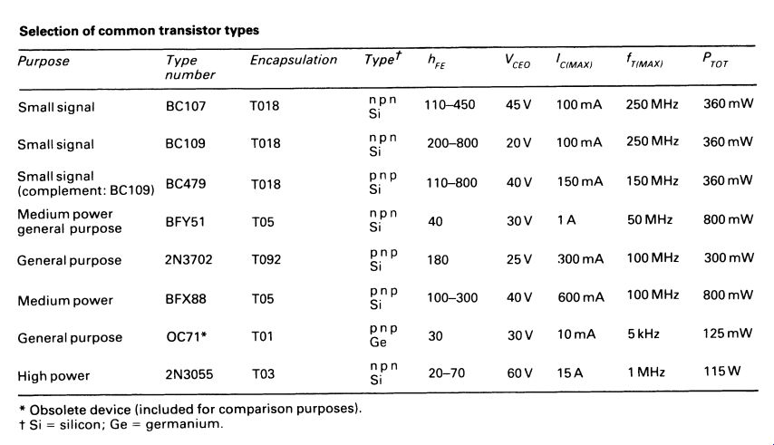
FIG. 16 table of some commonly used transistor types ------ Selection
of common transistor types
All six of these common case types are shown in FIG. 15.
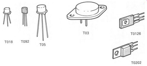
FIG. 15 six common types of transistor encapsulation
5. SOME TYPICAL TRANSISTORS
FIG. 16 gives a table of some common transistors likely to be found in any good electronic component shop.
Next, we will look at the second major class of transistors, the field-effect transistor (FET).
QUESTIONS
1. Which terminal of a bipolar transistor is common to both input and output circuits in the most commonly used configuration?
2. How do you calculate the current gain of a transistor?
3. Should the emitter be more positive or more negative than the collector in (i) pnp, (ii) npn transistors?
4. Describe the Early effect.
5. What is the leakage current?