AMAZON multi-meters discounts AMAZON oscilloscope discounts
Although devices that combine light with electronics are by no means new, the name 'optoelectronics' is recently coined. The same revolution that replaced the valve with the transistor, and subsequently complex transistor circuits with integrated circuits, produced an increase in the number and types of devices combining light and electronics. The term 'optoelectronic' came into use as a description for what has now become a large and important branch of electronics technology.
In a way the television picture tube and the neon lamp are both opto electronic devices, but the name does not apply to them in general usage because they are 'vacuum-state', not solid-state, devices. Optoelectronics refers to the new generation of solid-state components, and also to some of the components used with them.
1. LIGHT-EMITTING DIODES
Easily the most common optoelectronic device is the light-emitting diode (LED) which was discussed briefly at the end of Section 7. The LED is cheap (two or three for the price of a cup of coffee) and uses little power, so has found applications wherever an indicator lamp is required. Electrical and electronic equipment of all kinds use LEDs as indicators. The most usual color is red, but yellow and green are also available, like the pn diode of the normal non-light-emitting variety, the LED exhibits a forward voltage drop when conducting. This varies according to the type of semi conductor used, so voltage drops differ slightly. Typical values are around 2 V for red and 2.5 V for green or yellow. The usual type of LED used as an indicator light is 0.2 inch diameter or 1/8 inch diameter. The light output is usually around 2 mod for a current of 10 mA: not actually very bright, but enough for an indicator in all but the very brightest ambient light.
There is a photograph showing typical LEDs in Figure 7.13. LEDs are very easy to use in circuit, and have an indefinite life if used correctly. There are just a few rules that need to be remembered when using them:
1. The LED has no inherent current limitation, and must have a resistor (or something) in series with it to limit the current passing through it to the manufacturer's recommended safe value.
2. LEDs have a low reverse breakdown voltage, so must be protected from voltages applied in the 'wrong' direction. The simplest way to do this is to connect a diode in parallel with the LED, but facing the other way. Fig. 1 shows a typical circuit that permits the LED to be operated with an alternating current supply. The value of the resistor is chosen to provide an average current suitable for the LED. At mains frequency this circuit will cause a perceptible flicker, as the LED is being pulsed fifty times a second, with an 'off' period equal to the 'on' period.
3. The LED emits light over a fairly narrow band of wavelengths, so it is unfortunately not practicable to use filters over the LED to produce different colors. Red, yellow and lime-green seem to be the extent of the repertoire so far.
4. The LED has no time lag on the production of light (such as there is on a normal tungsten filament lamp) and so can be switched on and off very rapidly.
5. A small LED can generate a very bright pulse of light if it is brief. The standard 0.2 inch LED can be used to produce short pulses at much higher operating current than the rated maximum for continuous current. The manufacturers will give information, but typical figures for a 0.2 inch red LED would be 300 pulses per second, 1 uS in duration, with pulse current of 1A.
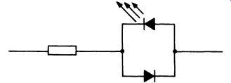
FIG. 1 circuit for operating a LED from an a.c. supply
The LED can easily be combined with a small integrated circuit; flashing LEDs use an internal IC, as do constant-current LEDs, which require no current limiting resistor and work over a range of voltages.
LEDs are often used in multiple displays- a LED 10-bar DIL array is shown in the photograph in Figure 7.13 . The circuit for this is shown in Fig. 2.
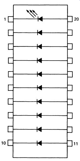
FIG. 2 a 10-LED bar graph display
The bar array is designed so that it can be stacked with other identical arrays, to make a bar graph display of any length required. Such indicators are often used for record level meters on hi-fi tape decks, as they are cheaper, more accurate, more robust and have more 'sales appeal' than ordinary mechanical meters. Special-purpose ICs are made for driving bar arrays.
LEDs are also used for the familiar 7-segment display, of the kind commonly used in digital alarm clocks. The 7-segment display can be used to produce any of the digits 0-9, and a very limited number of letters. The basic form of the display, together with a set of digits and letters, is given in Fig. 3.

FIG. 3 a basic 7-segment display, along with some of the characters
that can be produced
A typical alarm-clock display, equipped with hours, minutes and seconds, would require six 7-segment displays. If they were all connected like the one in Fig. 3, with seven connections to the bars and a common anode or cathode, there would be eight connections to each digit, or forty-eight connecting wires altogether. This is not very economical, and is wasteful of power, when you consider that at 12 : 58 :58 there will be no less than thirty-one segments illuminated, each taking about 15 mA, a total current consumption approaching half an amp, and a power dissipation, in the LEDs alone, of nearly 1 W. In practice the display is multiplexed, and is connected as shown in Fig. 4.
This cuts the number of wires down to thirteen, and only adds one more wire for each extra digit. The circuit driving the display is specially designed to make use of the display economically, and in practice only one digit is illuminated at any one time. The cathodes of the relevant segments for the first digit are switched to the power supply, and the digit-I anode is made positive for a short time. The digit-I anode is then disconnected and the cathodes switched in a suitable pattern for the second digit. The digit-2 anode is now made positive for a short time, and the sequence repeated over and over for each digit in turn.
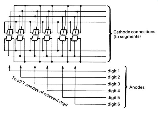
FIG. 4 multiplexing a 6-digit 7-segment display
Only one digit is ever on at any one time, but if the sequence is repeated at a high-enough speed, the human eye's persistence of vision will make it look as if the six digits are all lit up together. The multiplexing frequency is usually in the order of 1 kHz or so.
LEDs are commonly produced to emit light in the infra-red region, and infra-red LEDs are actually more efficient in output for a given current than LEDs operating in the visible part of the spectrum. Infra red LEDs are widely used for remote control and sensing applications, described later in this section.
2. LIQUID CRYSTAL DISPLAYS
Although LEDs are relatively efficient when compared with filament lamps they nevertheless use a lot of power compared with some types of IC. Early digital watches used LED displays, and even with low-brightness, high-efficiency multiplexed displays, the LED display still used a few milli amps, much too much to be left on all the time. These early watches there fore featured a 'black face', on which the digital time was displayed for a second or so when a button was pressed. Manufacturers of watches (and calculators) searched for a really low-power display system that could operate for a long time-at least a year-from a battery small enough to go inside a wristwatch. The solution proved to be the liquid crystal display (LCD). The LCD is unlike the LED in that it does not emit light, but is read, like the page of this guide, by reflected light. The typical form is similar to that of a 7-segment LED display, and is illustrated in Fig. 5.
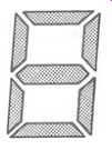
FIG. 5 a typical 7-segment LCD
The connections to the LCD are reminiscent of the LED display, but the actual operation is completely different. The usual kind of LCD, called a 'twisted nematic' display, works by means of polarizing light.
(There is another kind of LCD, called a 'dynamic scattering' display, but it is seldom used as it tends to have a shorter life, and produces rather curious milky-white characters against a dark background-harder to read than the more common twisted nematic display.) Most people are familiar with polarizing sunglasses. These polarize the light passing through the lenses so that the light waves move in one plane only. If an identical pair of sunglasses is placed in front of the first, there will be only moderate darkening of the beam passing through both, because the planes of polarization are the same. If, however, the second polarizing lens is placed so that the plane of polarization is at right angles to the first one, the light ray will be blocked completely. Fig. 6 shows the principle.
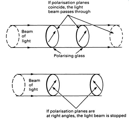
FIG. 6 if light is passed through a polarized filter, it will then
pass through subsequent polarizing filters only if the plane of polarizations
is the same; if the planes of polarization are at right angles, the light
will be blocked
A cross-section of the LCD is shown in Fig. 7a. Two thin pieces of glass are separated from each other by a plastic seal, and are held a precise distance apart, in the order of 10 um or so. The space between them is filled with the liquid crystal (really a liquid). On the inside of each piece of glass is a thin coating of a transparent conducting film. The pattern in which the film is printed produces the required display (see Fig. 7b).
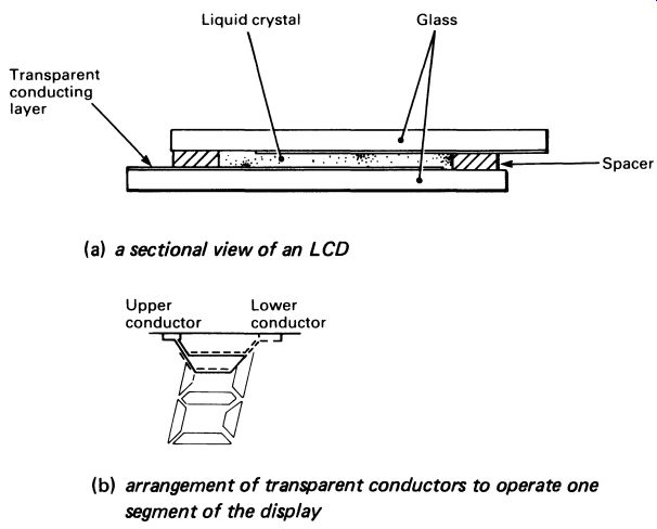
FIG. 7 -------- (a) a sectional view of an LCD ; (b) arrangement
of transparent conductors to operate one segment of the display
The liquid crystal has the property of rotating the plane of polarization of light passing through it. The amount of rotation depends on the precise composition of the crystal and on the thickness of the crystal--40 ~-tm will give a full 360°C rotation in a typical material. Thus 10 um thick crystal will rotate the plane of polarization through 90°. Behind the LCD is placed a piece of reflective polarizing material (like polarized sunglasses with a mirror behind them!), and in front a piece of transparent polarizing material. The planes of polarization of the two polarizers are at right angles to each other, and in normal circumstances any light reflected off the rear polarizer would be blocked by the front one. However, the 90° twist imparted by the liquid crystal rotates the plane of polarization of the light so that most of the light falling on the display from the front is reflected back again, and the LCD appears to be completely transparent. You can even see the polarizing reflector behind the display if you look carefully -but try looking at the display of a LCD watch through polarizing sunglasses, rotating the glasses to see the effect of changing the plane of polarization! If the display is energized by means of an electric voltage applied between the two transparent conductors controlling one of the segments, the situation changes. The liquid crystal is an insulator, so there is practically no current flow; but the electric field that appears between conductors that are opposite to each other affects the crystal, changing its regular structure in such a way that it no longer rotates the plane of polarization of light passing through it. Light reflected off the rear polarizer therefore reaches the front polarizer with its plane of polarization 90° out-and fails to pass through it. Viewed from the front, the energized segments appear black against the bright reflected light of the polarizer. The principle of operation is shown in Fig. 8.
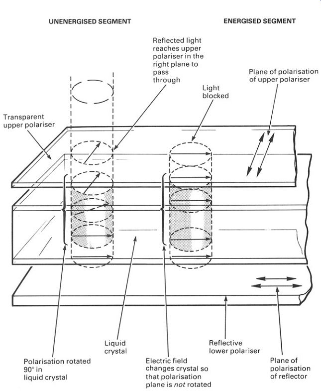
FIG. 8 principle of the LCD (twisted nematic type)
The LCD has the big advantage that, like the field-effect transistor, it does not need a current flow to work, and power requirements are there-fore tiny. A large (12 mm high) LCD with four digits would draw less than 5 uA from a 3 V supply.
In addition, the LCD works in bright light (the LED display watch is hard to read in the sunshine) and can be illuminated with a yellow LED or tiny incandescent lamp for the rare occasions in which it will need to be read in the dark.
Good ideas are rarely without drawbacks, and the drawbacks of the LCD are relatively few. But it does require an alternating voltage to energies the segments, not because they will not work with direct voltages, but because a direct voltage damages the crystal over a relatively short time. Where the LCD is driven by an IC designed for the purpose, this is no problem at all, but in circuits made with discrete components it calls for slightly more complication. Second, the LCD is not as robust as the LED display, and a hard knock will break the glass. In watches, careful case design minimizes the chance of breakage.
Since the shapes of the energized segments of the LCD are printed on to the glasses, there is no limit to the kind of picture that can be built up. Where letters and number are required, it is practical to use a dot matrix LCD. The details vary, but the design shown in Fig. 9 is widely used. A wide range of numbers, letters and special characters can be built on to the dot matrix.
FIG. 9 dot matrix displays
The same limitations on connections apply to LCDs that apply to LED displays, although LCDs are less commonly multiplexed than LED displays. Multiplexed displays are made only where very large numbers of separate segments or dots are needed, as the LCD uses so little power that multiplexing is unnecessary, except to save connections.
LCDs are quite unlike LED displays in the speed of response, for the LCD is a relatively slow device, taking at least tens and sometimes hundreds of milliseconds to respond.
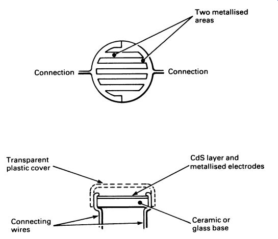
FIG. 10 a typical photoresistor (CdS cell)
3. PHOTO-SENSITIVE DEVICES
The photo-conductive cell (photoresistor)
All semiconductors are sensitive to light, to a greater or lesser extent. It is for this reason that transistors and diodes are packaged in light-proof encapsulations, either metal or plastic.
Certain components make use of the light sensitivity, and are designed to be used as light-detecting devices. There are several different basic devices, but the simplest and one of the most commonly used is the photo conductive cell, or photoresistor.
When light falls on a semiconducting material, some of it is absorbed.
The energy that this imparts produces an electron-hole pair, and the free electron and hole are available for carrying current through the semi conductor, reducing the electrical resistance. The electron and hole are usually formed in the valence band (see Section 6), which is where the current flows. The amount of energy delivered by the light falling on the semiconductor is important, and since light of different wavelengths provides different amounts of energy, the semiconductors are selective in the frequencies of light that they respond to. Almost all semiconductors, including germanium and silicon, respond to light in the infra-red region.
This is generally unimportant, except where the response of the photo resistor must parallel the light response of the human eye.
Just one material responds in the region of visible light, and this is cadmium sulphide. Cadmium sulphide (usually referred to by its chemical symbol of CdS) is sensitive to about the same range of frequencies as the eye, and is commonly used in camera exposure control systems.
Physically, the CdS photoresistor is no more than a thin layer of cadmium sulphide on a ceramic base, with metal (usually aluminum) connections printed on top. The electrodes are made with a characteristic interlocking comb layout, to maximize the length of the 'junction' in relation to its width. Fig. 10 illustrates the design.
In the dark the CdS photoresistor has a high resistance, and the ORP12, the standard 'large' photoresistor, has a dark resistance of 10 M-ohm. In bright sunshine the resistance can drop as low as 150 Q, or even less. In terms of electronics this is a massive range, which probably accounts for the rather small number of different designs produced by the different manufacturers. The ORP12 and the smaller ORP60 take care of most requirements.
CdS photo resistors can dissipate moderate amounts of power, for example the ORP12 can dissipate up to 200mW. They can also be used with relatively high voltages; the ORP12 can survive 110 volts maximum.
Because the design is symmetrical, the photoresistor is unaffected by polarity of applied voltage and can be used with alternating or direct voltage supplies.
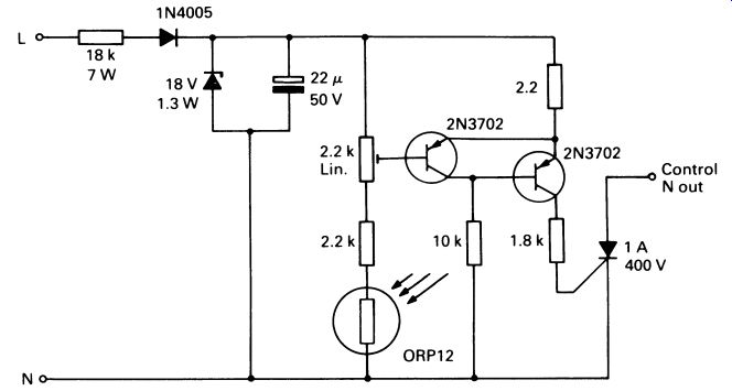
FIG. 11 a practical circuit to turn a mains-operated light on at
dusk and off at dawn: caution-see text before attempting to build this
project
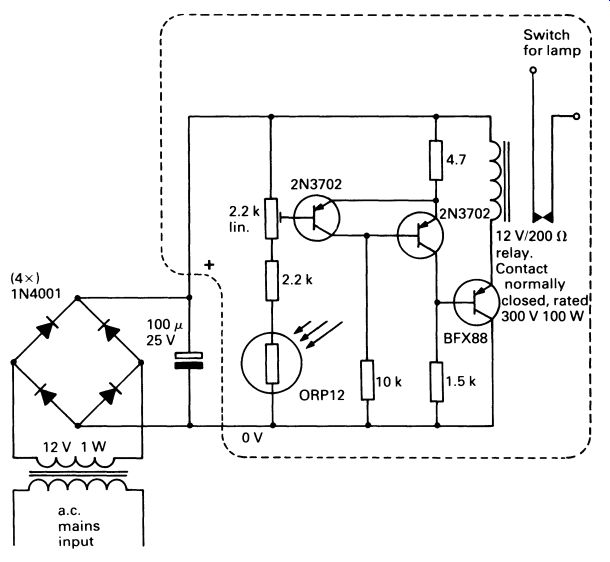
FIG. 12 a lighting-control circuit using a transformer and relay
for added safety
Fig. 11 illustrates the CdS photoresistor in a typical application, turning a mains voltage lamp on when it gets dark and off again at dawn.
The circuit symbol is shown with the three arrows denoting 'light'. The circuit of Fig. 11 is completely practical and can be made as a project. Notice, however, that the circuit is live to the mains supply and must be properly insulated. If in any doubt about safety, do not con struct this circuit, or at least get expert advice about insulation. Note also that the 7 W resistor gets hot. This circuit uses a thyristor to control the mains; the triac is described in Section 17. The light-control circuit is given as an example of a typical 'commercial' application. It is interesting to compare the circuit of Fig. 11 with that of Fig. 12, which does a similar thing, though rather more safely.
In the circuit of Fig. 12 a transformer power supply operates the same basic phototransistor circuit, and the mains is switched by a relay (also dealt with in Section 17). The photoresistor circuit is operated at low voltage, and less heat is dissipated. For reasons of cost, the circuit of Fig. 11 would be preferred by a manufacturer, who could make sure that the insulation met the required standards. Fig. 12 makes a good project; even so, you must observe stringent safety precautions as mains is still present on the primary of the transformer and also the relay.
If you are in any way unsure about safety, then the part of the circuit in the dashed box in Fig. 12 can be made, and will work with a 12 V battery.
Although photoresistors have many uses, they respond to changes in light rather slowly, and so are unsuitable for control applications, or other applications where rapid response to light level is required.
Photo diodes
A photodiode is structurally very similar to a normal pn junction diode, though there may be a mechanical differences, brought about by the necessity to maximize the area of the junction that can be exposed to light.
Photodiodes are used in a reverse-biased mode, and the leakage current will then depend on the amount of light falling on the device. Photo diodes are useful for measurement applications, since the leakage current is directly proportional to the light intensity over a wide range.
Silicon is generally used for photodiodes, so the peak response to light is in the infra-red region. The actual amount of current is also rather small. A typical photodiode might have a dark current of 1.5 nA, and an output current in bright sunshine of 3.5 uA. Quite substantial amplification is therefore required for most applications, and this would usually be provided by an op-amp.
Photo transistors
In the same way that the photodiode is very like a normal pn junction diode, so the phototransistor is very like a normal bipolar junction transistor. Apart from a transparent encapsulation (a metal case with a glass or plastic window in the top, or, more cheaply, solid transparent plastic) and possibly mechanical changes to expose more of the junction area to light, there is no difference. The base-emitter junction is either left disconnected or is slightly reverse-biased, and the junction operates as a pn photodiode. However, the collector current is amplified in the normal way, and so may be up to two or three hundred times larger than the output current of the photodiode. A typical silicon phototransistor might have a leakage current (base open-circuited) of a few tens of nanoamps, and a collector current of 500 uA in bright sunlight.
It is also quite common to combine two transistors in one, to make a photo-Darlington, such as the 2NS777 illustrated in Fig. 13. In the Darlington pair configuration the gain of the two transistors is multiplied together, so the output of the photodiode is multiplied by at least 10000. Photo-Darlington transistors are inexpensive and are usually preferred to a photodiode or phototransistor with extra amplification. The photo Darlington can be connected directly to CMOS logic circuits when used with reasonable illumination levels--this is useful for applications involving counting objects, as you will see in Section 23.
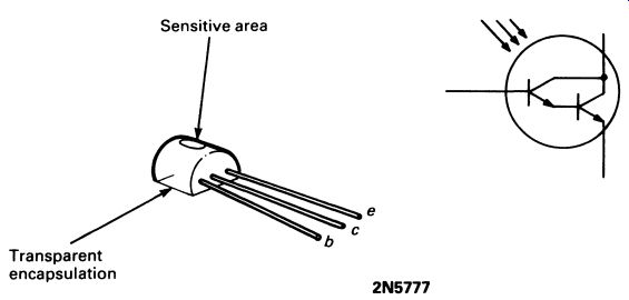
FIG. 13 a photo-Darlington transistor
Photosensitive ICs
A number of devices go further than the photo-Darlington, and combine a photosensitive junction with an amplifier and switching or shaping system. This, as usual with ICs, reduces the component count substantially with only moderate increase in the cost of the basic device. A typical example of the kind of thing that can be done is the LASSV light-activated switch IC. This incorporates a high-gain amplifier and switching circuits that ensure a very rapid transition from the 'on' to the 'off' state and back again. Two external components are required, to set the thresholds for switching. The LASSV provides an output that is directly compatible with CMOS or TTL logic circuits, or will even drive a small relay directly.
Examples of both applications are given in Fig. 14.
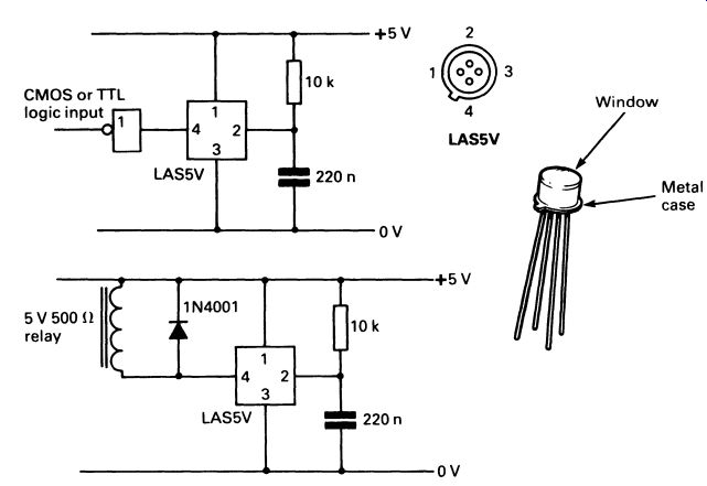
FIG. 14 a photosensitive IC; this can be used to drive small relay
or logic circuits
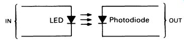
FIG. 15 an opto-isolator
It should by now be clear that the general principle of photosensitivity can be applied to practically any semiconductor device all that is necessary is to expose the relevant junction to light. A range of photosensitive devices of a specialist nature--photothyristors and phototriacs, for example (see Section 17)--are available.
The most widely used devices are photoresistors, photo-Darlington transistors, and various light-sensitive ICs.
4. OPTO-ISOLATORS
The opto-isolator (sometimes known as an opto-coupler) combines the LED and photodiode or phototransistor.
Since both the LED and the phototransistor (or photodiode) can respond very rapidly to changes in applied current/light, it is possible to used a LED placed close to a phototransistor to provided an information link that is completely isolated electrically. The scheme is illustrated theoretically in Fig. 15.
This kind of component is useful where circuits are at widely different potentials but need a signal to be passed from one to the other. The opto isolator is a substitute for the isolation transformer in this application, but it is more efficient. A small opto-isolator in a DIL pack can easily provide isolation between circuits at potentials differing by up to 4 kV. Opto-isolators are also valuable for feeding signals into sensitive circuits.
If, for example, an electrically 'noisy' line (a line on which may be super imposed high-voltage interference spikes) is required to feed an NMOS or CMOS circuit, directly connecting the two could well cause the sensitive NMOS or CMOS circuits to be destroyed by the interference. An opto isolator provides the required coupling of the signal in complete safety.
The efficiency of an opto-isolator is stated in terms of the transfer ratio, which is simply the ratio of the output current to the input current, expressed as a percentage. A transfer ratio of 100 percent would therefore provide an output current of 1 mA for each 1 mA of input current to the LED. Opto-isolators using photodiodes would have transfer ratios of less than 5 percent. Those using phototransistors are generally made with transfer ratios of 20 percent, and those using photo-Darlington transistors can have transfer ratios better than 500 percent-amplifying the input current by 5 times.
The frequency response is quite good, up to 200-300 kHz, according to type. Maximum currents are of course limited by the maximum rating of the LED and the maximum dissipation of the transistor.
5. PHOTOVOLTAIC CELLS
Commonly known as 'solar cells', photovoltaic cells convert light energy directly into electrical energy.
Early photovoltaic cells were very inefficient in terms of energy con version, and produced very small currents and voltages. Since the 1960s intensive development has taken place, partly because it is thought that in some applications solar power, generated by means of photovoltaic cells, is a useful source of energy. This may yet prove to be true, but the most immediate use (and the reason for the large development budgets) is in the powering of space vehicles. In the inner solar system the sun represents a useful source of free energy for a space vehicle, an energy source that involves no payload of fuel, and will not run out in the anticipated lifetime of the space vehicle. Telecommunications satellites are invariably powered by photovoltaic cells, and the present designs are surprisingly efficient, converting about 20 percent of the light energy falling on them into electrical power.
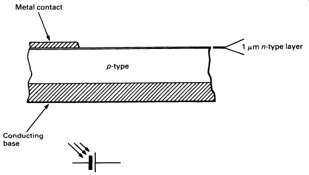
FIG. 16 a silicon solar cell, along with its circuit diagram
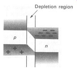
FIG. 17 energy-level diagram for a pn junction
The structure of a silicon photovoltaic cell is shown in Fig. 16.
An energy-level diagram for the pn junction exhibits the characteristic depletion region (Fig. 17: refer to Sections 6 and 7 if you need to) in which there are no holes or free electrons.
If, however, light is able to reach the junction, the energy absorbed from the light will break some of the bonds between adjacent atoms in the junction region, resulting in the formation of electron-hole pairs. These have to leave the depletion region immediately, and, if the two sides of the pn junction are connected through an external circuit-the load-they will flow through that circuit as an electric current (Fig. 18). Silicon photo voltaic cells are made with a very thin layer of n-type semiconductor on the 'top' layer, the n part of the pn junction. The layer may be only 1 um thick, and is thin enough to allow incident light to penetrate to the junction region easily, resulting in a cell that is extremely efficient compared with older devices.
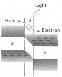
FIG. 18 generation of electric current in the pn junction of a photovoltaic
cell
A silicon photovoltaic cell in the 'average efficiency' range, about 10 em diameter, might well produce a current of 2 A in bright sunlight, with a potential of around 0.5 V. Since roughly 1 kW falls on every square meter of the earth's surface, this means that just under 8 W falls on the cell.
With an output of 1 W, this means that the efficiency is about 12 percent. Silicon photovoltaic cells are not cheap, and the most efficient types would be used only for defense and aerospace applications.
6. FIBER-OPTIC SYSTEMS
Although not strictly electronic in nature, fiber-optic systems are import ant in communications applications. The fiber itself is a long 'wire' made of special glass or plastic. The outer layer has a different refractive index from the inner core, and if a light is shone on one end of the fiber, it will be transmitted down the whole length of the fiber to emerge at the other end with remarkably little loss of brightness. With careful fiber design and the correct wavelength of light applied to the end, attenuation can be reduced to as little as 30 dB per kilometer, for relatively inexpensive fiber. A suit able LED is used as the light source, and a photodiode as the detector. The system is shown in outline in Fig. 19.
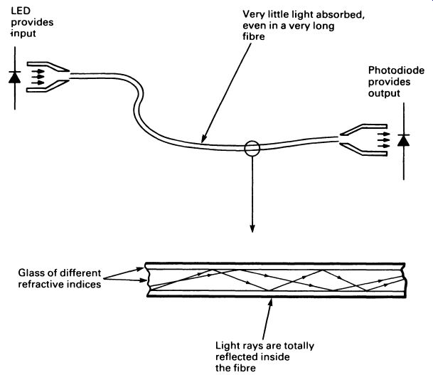
FIG. 19 principle of a fiber-optic data-transmission system
Very large bandwidths-up to 50 MHz even in inexpensive systems-can be obtained, more than can normally be obtained with conventional cables. Compared with copper cables, a telecommunications system using fiber-optics has many advantages. These include complete freedom from electromagnetic interference, complete electrical isolation, freedom from crosstalk (parallel cables inducing signals in one another, resulting in 'crossed lines'), low weight, greatly increased security (it is very difficult to 'tap' a fiber-optic phone line), and eventually cheapness (glass is basically a much cheaper material than copper). The future of long-distance communication, apart from radio, seems to lie much more in fiber-optic systems than in transmission by means of electrical signals.
7. LASER DIODES
Although LEDs emit light over a narrow band of frequencies, the design of fiber-optic systems for use with LEDs is something of a compromise as the range of frequencies emitted by a LED makes it impossible to design the 'ideal' system. The reason for this is obvious if you consider a rainbow, and Newton's experiment with the prism - the amount by which light is refracted as it passes through a transparent medium depends on its frequency. This causes scattering, known as chromatic aberration, in any optical system involving refraction. A truly monochromatic light (a light consisting of a single frequency) can be focused to the theoretical limits of accuracy by a relatively simple lens, and the refractive indices of a fiber optic system can be chosen to give near-perfect light transmission.
It is possible to generate monochromatic light at a high brightness level by means of a semiconductor LASER. The name LASER is another acronym, from Light Amplification by Stimulated Emission of Radiation.
Lasers come in a whole range of sizes. The most powerful types have been used experimentally to shoot down aircraft in flight (although they are still a long way from the kind of thing you saw in Star Wars); semiconductor Lasers, even the biggest, are much more modest affairs, having a light output at most a few tens of times more intense than a LED. Both the theory and the structure of a semiconductor laser are complex. Fig. 20 shows, in diagrammatic form, a typical gallium arsenide laser diode. There are five layers of semiconductor. The central layer of p-type aluminum gallium arsenide has a thin strip of p-type gallium arsenide down the center, and it is in this thin strip, about 1 um by 10 #lffi, that the laser action takes place.
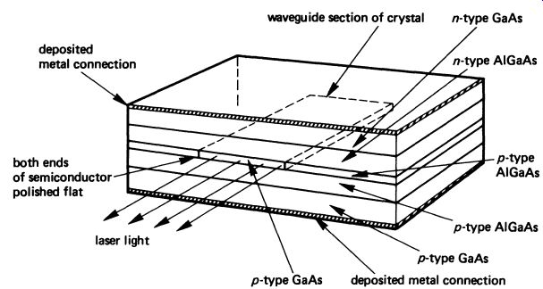
FIG. 20 physical structure of a gallium arsenide semiconductor LASER
------- (NOTE GaAs = gallium arsenide; AlGaAs =aluminum gallium arsenide)
Without going into too much detail, it works like this. Light is generated at the pn junction in the normal way (see Section 7 .8) and this light enters the thin strip of p-type gallium arsenide. Because the central strip has a higher refractive index than the material on either side, it behaves just like the fiber-optic light guide -light is trapped inside the strip. If the light in the strip is sufficiently intense, laser action begins. Photons are reflected backwards and forwards across the crystal, the ends of which are polished exactly flat and parallel. Some photons will collide with electrons in the conduction band. When this happens 'stimulated emission' can occur, releasing two photons travelling in exactly the same path. Both photons can now collide with electrons in the conduction band, and the result can be four photons, all in phase with each other and thus at the same frequency. The result is a rapidly increasing avalanche of photons, all trapped within the crystal. These photons eventually emerge from the end of the crystal as an intense beam of light at a single frequency. The light is also coherent, that is, the waves are all in phase with each other.
The monochromatic light source provided by the semiconductor laser is perfect for opto-electronic communications systems, and is also used in compact disc players (see Section 18.1) where it can be focused into a tiny circle less than 2 um wide to 'read' the CD track.
QUESTIONS
1. Why is multiplexing often used in circuits operating LCDs?
2. When would a LED display be used instead of a LCD?
3. Suggest three circuits in which you might use a photo resistor.
4. When are opto-isolators used?
5. If solar cells can be used to power satellites and spacecraft for years at a time, why can they not be used to power cars?