AMAZON multi-meters discounts AMAZON oscilloscope discounts
Field-effect transistors are a more recent development than bipolar transistors, and make use of a completely different mechanism to achieve amplification of a signal. Field-effect transistors (FETs) are unipolar, and involve only one type of charge carrier (electrons or holes) in their operation. There are also two major types of FET, junction-gate field-effect transistors (JUGFETs) and insulated-gate field-effect transistors (IGFETs). There are, as we shall see, subdivisions within these two classes.
Operationally, FETs are more similar to valves than are bipolar transistors. The main distinguishing characteristic compared with bipolar transistors is the fact that they are voltage-controlled rather than current controlled. The circuit symbol is given in FIG. 1; a voltage applied to the gate is varied to provide a corresponding charge in the resistance between the source and drain.
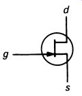
FIG. 1 circuit symbol for an n-channel field-effect transistor
Unlike the bipolar transistor's base connection, the gate of the FET has a very high input resistance, at least a few tens of megohms and in some cases, gig-ohms. The amount of current drawn by the gate is therefore extremely small.
FETs can be used in amplifier circuits, just like bipolar transistors.
Compare the circuit of FIG. 2, which shows a typical JUGFET, with that in Figure 8.5 . The difference is the lack of a gate (base) resistor; because negligible current flows in the gate connection, such a resistor would make no difference to the operation of the circuit, adding a moderate amount of resistance to one that is extremely large in the first place. Just as there are n-type and p-type resistors, so there are n-channel and p-channel JUGFETs. FIG. 3 shows a p-channel version, while those in Figures 1 and 2 are n-channel. As in the case of bipolar transistors, practical operation is the same but with all polarities reversed.
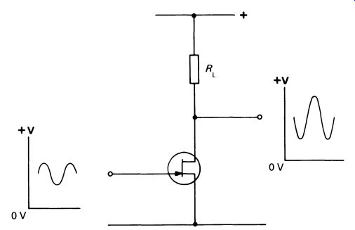
FIG. 2 a simple amplifier using an n-channel FET
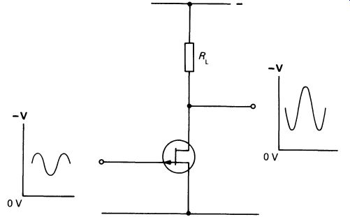
FIG. 3 a simple amplifier using a p-channel FET (note the different
polarity of the power supply, compared with FIG. 2)
1. FET PHYSICS
The JUGFET has a physical structure that can be represented by a diagram like the one in FIG. 4, though in practice it is not easy to diffuse impurities with both sides of the wafer, and a rather different layout is used. Section 11 gives details.
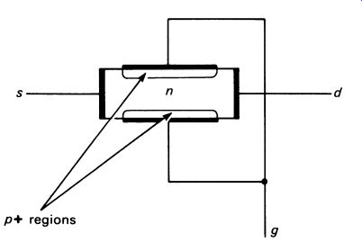
FIG. 4 theoretical construction of an n-channel depletion-mode
FET
A bar of n-type semiconductor (almost invariably silicon) is made with shallow p-type regions in the upper and lower surfaces. These are connected to the gate terminal, and the two ends of the bar are connected to the source and drain.
If the bar is connected to a voltage source, current will flow through it.
Since the bar is symmetrical, it can flow either way, the source and drain being interchangeable. The current flow consists of electrons moving through then-type semiconductor (FIG. 5).
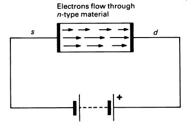
FIG. 5 movement of electrons with no voltage applied to gate.
Now observe the effect of a negative potential applied to the gate regions. The junction between the p and n regions forms a reverse-biased diode (see Section 7) so no current flows, but an electric field extends into the n-type bar from the p-type regions. This charge forces current carriers {electrons) away from the region, reducing the amount of bar available for conducting the current between the source and drain {shown diagrammatically in FIG. 6).
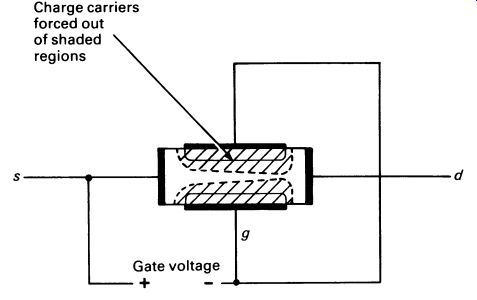
FIG. 6 the electric field forces charge carriers away from the plates
when a negative potential is applied to the gate
If the potential applied to the gate is made sufficiently negative, the electric field will extend across the whole thickness of the bar of n-type semiconductor, hardly any charge carriers will be available for current flow, and the current available from the drain will drop to a very low value (never to zero, for it is physically impossible for the channel to 'close' completely: see FIG. 7).
Changes in the voltage applied to the gate will cause corresponding changes in the current flowing between the source and drain, which makes the operation of the FET very similar to that of a bipolar transistor.
2. THE INSULATED-GATE FET
Generally known as a MOSFET (metal-oxide semiconductor FET), the insulated-gate FET is one of the most important devices in the electronics industry. There are two basic categories of MOSFET, known as depletion MOSFETs and enhancement MOSFETs. They work on a different principle from the JUGFETs that we have been looking at so far in this section.
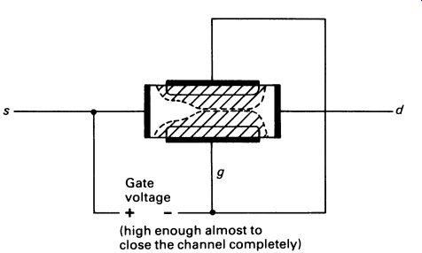
FIG. 7 although the current flow can be greatly reduced, it is impossible
to stop it completely-there will always be a small gap between the two
areas without charge carriers

FIG. 8 theoretical construction of an n-channel enhancement mode
FET (note that the gate is completely insulated from the rest of the
structure by a very thin layer of silicon dioxide)
The structure of a p-channel enhancement MOSFET--again, a theoretical structure--is shown in FIG. 8.
The most striking feature is the gate. It is insulated from the silicon by a thin layer of silicon dioxide. The layer is very thin, typically only about 0.1 um thick. Although very thin, the silicon dioxide layer has an extremely high resistance, so the gate input resistance is very high indeed, at least 10 G-Ohm.
The n-type silicon has two regions of heavily doped p-type impurity, connected to the source and drain. With no applied gate voltage, one of the p-n junctions (depending on which way round the source and drain have been made) will act like a reverse-biased diode and block any flow of current. If a negative potential is applied to the gate electrode, holes from the p-type regions are attracted into the area immediately beneath the electrode. This effectively, if temporarily, makes a narrow p-type region just beneath the gate, illustrated in FIG. 9.
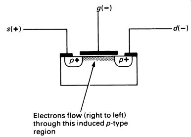
FIG. 9 a p-type region is induced in the n-type bar when the gate
is made negative.
The blocking p-n junction is bypassed by this induced channel of p-type material, and electrons can flow through the device, between the source and drain. The circuit symbol for the p-channel enhancement MOSFET is given in FIG. 10. The center connection in the circuit symbol (with the arrowhead) is a connection to the silicon substrate (the chip itself). Often the connection is made internally to the source, but sometimes manufacturers fit a fourth lead so that the substrate can be used as a second 'gate', the conduction characteristics of the device then depending approximately on the difference in potential between the gate and substrate.

FIG. 10 circuit symbol for a p-channel enhancement MOSFET
When the circuit symbol has an arrowhead pointing away from the gate, it symbolizes a p-channel device. It is, however, equally possible to make an n-channel device, with all the polarities reversed, using n-regions diffused into a p-type bar. In this case the charge carriers are electrons attracted from the n-regions; otherwise operation is the same. The circuit symbol for an n-channel enhancement MOSFET is given in FIG. 11.
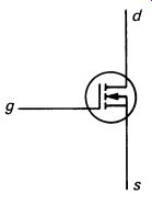
FIG. 11 circuit symbol for an n-channel enhancement MOSFET
The second class of MOSFET is the depletion MOSFET. The structure is shown in FIG. 12, and is similar to that of the enhancement MOSFET. Notice that there is an 'extra' region. A narrow strip of p-type impurity has been diffused into the space below the gate, so that the depletion MOSFET, with no signal applied to the gate, looks rather like the enhancement MOSFET when its gate is connected to make it conduct. Compare Figures 12 and 9.
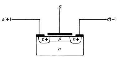
FIG. 12 theoretical structure of a depletion MOSFET
Applying a positive signal to the gate causes electrons from the n-type region to be attracted to the area under the gate electrode, neutralizing some of the holes in the p-type channel and reducing the amount of current flowing between the source and drain. The higher the positive potential (for a p-channel device, of course), the more the source-drain current is cut off.
Actually the depletion MOSFET can also be used in the enhancement mode as well. Applying a negative voltage to the gate of a p-channel device will increase the source-drain current by adding to the number of holes available as charge carriers. FIG. 13 shows the circuit symbols for p-channel and n-channel depletion MOSFETs.
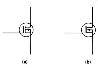
FIG. 13 circuit symbols for (a) p-channel and (b) n-channel depletion
MOSFETs
3. USES OF MOSFETs
At first it seems paradoxical that, even though the MOSFET is a vitally important device, individual MOSFETs are rarely used. Only in the highest quality communications receivers do we find MOSFETs used as a matter of common practice. MOSFET technology is used overwhelmingly in integrated circuits.
Before leaving FETs for the time being, let us just look at one or two interesting aspects of the devices:
(1) Because of the necessity for a very narrow channel, it is difficult to make FETs that will carry high currents. Most FETs are therefore low power devices.
(2) Very high frequency operation of FETs is hampered by the internal capacitance, a byproduct of the very narrow regions. There is an effective capacitance of a few picofarads between the source (and drain) and the gate.
(3) It is possible to make FETs very small.
(4) Because of the very high input resistance and the thinness of the silicon dioxide insulating layer, MOSFETs are very liable to damage from high voltages accidentally applied between the gate and the other terminals.
For this reason, most MOSFETs are made with a Zener diode connected between the gate and substrate. Normally, the Zener diode is non-conducting, but if the gate voltage rises too high, it conducts and discharges the gate. Even so, MOSFETs are easily damaged by electrostatic voltages. The charge on a person wearing shoes with rubber or plastic soles can rise, on a dry day, to several kilovolts. This is often enough to destroy the MOSFET, Zener and all. Even touching the gate terminal can therefore destroy the device! The terminals of a MOSFET are generally shorted together with metal foil or conductive foam until it is installed in a circuit. Extra care is needed when servicing any equipment that might include MOSFETs.
QUESTIONS
1. What is the major difference in characteristics between IGFETS and JUGFETs?
2. Special precautions are needed when handling IGFETS--why?
3. Why are high-power FETs uncommon?
4. Draw the circuit symbols for (i) p-channel enhancement FET, (ii) n-channel enhancement FET, (iii) p-channel depletion FET, (iv) n-channel depletion FET.
5. What limits the higher frequency performance of FETs?