AMAZON multi-meters discounts AMAZON oscilloscope discounts
The last two sections showed how transistors-bipolar and FET -work as amplifying devices, using a small current or voltage to control a much larger current. The application to a machine like a record-player, for example, is an obvious one, for the small electric signal produced by the player's pick-up cartridge must be amplified to a sufficiently large extent to drive a speaker. A system diagram of a record-player amplifier looks quite simple (see FIG. 1). The symbols for the cartridge, amplifier and speaker are those conventionally used. In practice the amplifier is rather complex, and breaks down into two main sections: the preamplifier, which deals with the amplification of the small signal from the cartridge; and the power amplifier, which deals with the high-power amplification necessary to drive the speaker. Audio amplifiers are covered in more detail in Section 13, but in this section we shall look at typical techniques of small-signal amplification.
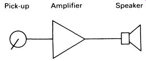
FIG. 1 system diagram for a record-player amplifier
Pick-up Amplifier Speaker
At its simplest a transistor amplifier circuit looks like the one in FIG. 2, but although this simple configuration is satisfactory for demonstrating 'transistor action', it is incapable of amplifying an audio signal.
Consider the effect of applying the alternating voltage from the pick-up cartridge to terminal A as shown. Since the transistor conducts only when the base-emitter junction is forward-biased, only the parts of the signal that are positive relative to the emitter will cause the transistor to conduct.
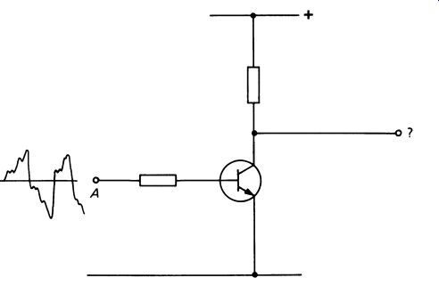
FIG. 2 the simplest form of transistor amplifier; this circuit could
not amplify an audio signal!
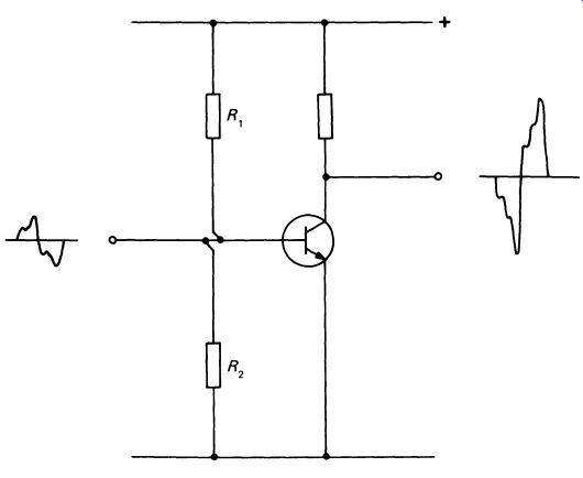
FIG. 3 a bias network for a transistor, enabling the transistor
to be used with audio signals (the resistor values would need to be altered
for each individual transistor).
As well as amplifying the input signal, the transistor is rectifying it. Occasionally this happens in an amplifier under fault conditions, and it sounds terrible! It is also clear that a proportion of the positive part of the signal is lost as well, since the transistor will not conduct, even with the base emitter junction forward-biased, until the potential exceeds 0.7 V for a silicon transistor. This is a substantially higher voltage than a magnetic pick-up cartridge produces, so in practice the output of the circuit in FIG. 2 would be zero.
A solution to the problem is simply to connect a suitable positive potential to the base, ensuring that it is always forward-biased. This is best done with a potential divider network involving two resistors, as shown in FIG. 3.
This does at least produce an output, if the two bias resistors R 1 and R2 are exactly the right values; the resistors should be chosen so that the collector is at half the line voltage with no signal applied. This gives approximately equal 'headroom' for the signal in its positive and negative excursions. Referring to the load lines in Figure 8.12 , it means that the operating point -that is, the mid-point of the variations in collector voltage when the amplifier is working-is halfway along the load line.
You should recall from Section 8 that because of tiny differences in manufacture it is not possible to specify the gain of a transistor very accurately, a gain variation of ± 50 percent being common. Using the circuit in FIG. 3 would mean careful measurements and a new pair of resistors for each individual transistor used-not an ideal requirement for mass production. The leakage current of the transistor, and thus its operating point, will also change with temperature. What is needed is a circuit that will automatically compensate for variations in gain of the transistor and ambient temperature. Such a circuit is shown in FIG. 4.
In this circuit it is the values of the resistors that determine the operating point. The gain of the transistor, leakage and temperature have practically no effect. The circuit involves a feedback loop. Feedback is a principle that is often used in electronics, and you will find it in many different contexts. In this case negative feedback is used. Negative feedback consists of a connection from the output of a system back to the input, arranged so that the change in output reduces whatever is causing that change.
Negative feedback improves the stability of a system, in that any change is counteracted.
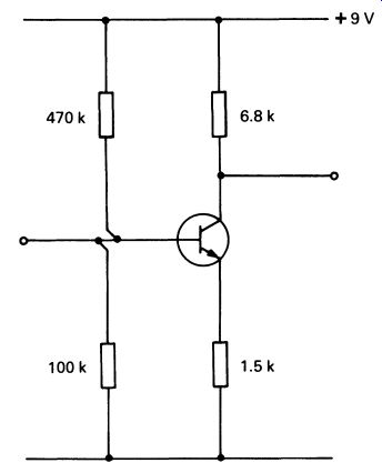
FIG. 4 an automatic bias circuit that will operate for a wide range
of transistor gains.
The opposite, positive feedback, makes a system less stable, as the effect of any change is augmented by the feedback.
Although the circuit of FIG. 4 looks simple, it is not immediately obvious how it works. Its operation is as follows. First, the base of the transistor is held at about + 1.5 V, high enough to overcome the 0.7 V potential barrier of the transistor's base-emitter junction if the collector is near 0 V. Consider what happens if the transistor were non-conducting; the emitter is connected to 0 V via the 1.5 k ohm resistor, and so is at 0 V.
However, this means that there is a potential difference of about 1.5 V across the base-emitter junction, so in practice the transistor is turned on and conducts.
A collector current is therefore flowing, and the collector resistor, transistor, and emitter resistor operate as a potential divider. Clearly the potential on the emitter will be higher than 0 V. Neglecting the voltage drop in the transistor, the emitter will be at a maximum potential of 1.5 V if the transistor is turned 'hard on' -but, of course, if the base and emitter are at roughly the same potential, there will be no base current, and the transistor will be off! In practice, the base current settles down to a fixed value, and in the circuit shown the collector will be 'balanced' at about half the supply voltage.
The compensating action of the circuit is easy to see. Assume that an increase in temperature causes the leakage current to rise and the transistor's collector-emitter resistance to drop. The resistance in the upper half of the potential divider (of which the transistor's emitter is the middle) will be lowered, and the positive potential on the emitter will rise, to become closer to that of the base. This will reduce the base current, and compensate for the temperature change. Transistors with different values of hFE are also compensated for in the same way.
A simpler but somewhat less effective bias circuit is shown in FIG. 5. In this design the bias is fed to the base via a resistor connected between the collector and base. Any tendency for the transistor to con duct more will reduce the positive potential at the collector, since the transistor and the 10k.Q load (collector) resistor form the two halves of potential divider. Ohm's Law indicates that this reduces the current flow through the 100 k-Ohm bias resistor, since the voltage across it is reduced.
Once again, we have a circuit in which any increase in the transistor's collector current causes a drop in base current.
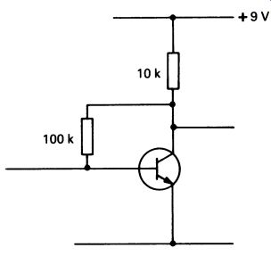
FIG. 5 a simpler circuit than that of FIG. 4, but sufficient
to provide automatic bias for silicon transistors in many applications
1. CAPACITOR COUPLING AND BYPASS CAPACITORS
When an amplifier is used to amplify an audio waveform, or indeed any other continuously changing quantity, the amplifier of FIG. 4 is connected to the input device (a pick-up cartridge was mentioned) through a capacitor. The purpose of this is to block any d.c. component in the input. FIG. 6 illustrates an amplifier circuit connected to a magnetic pick-up.
The pick-up provides a signal source, and this is coupled to the base of the transistor with a capacitor. The capacitor blocks any flow of d.c. which would otherwise interfere with the bias arrangements. If the capacitor were omitted, the resistance of the coil in the pick-up, typically just a few ohms, would be in parallel with the lower resistor in the base bias system. This would reduce the potential on the base almost to 0 V, which would turn the transistor off. For much the same reasons, the output of the amplifier would be coupled to the next stage of amplification with a capacitor.
Additionally, the emitter resistor reduces the efficiency of the amplifier by allowing the potential of the emitter to change with the signal being amplified. A large-value capacitor, connected across the emitter resistor, prevents the signal component affecting the bias conditions. An electrolytic capacitor is generally used for the emitter resistor bypass capacitor.
FIG. 7 illustrates a two-stage amplifier based on the circuit in FIG. 6, with capacitor coupling between stages. Note the difference in resistor values for each stage-the second stage has a larger input voltage swing than the first, and also delivers a higher output current.
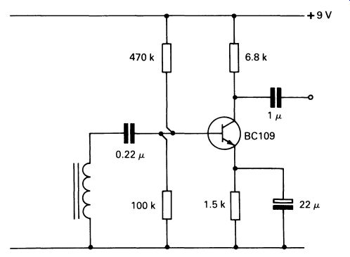
FIG. 6 a pick-up preamplifier; small capacitors couple the input
and output of the amplifier, and a large electrolytic capacitor is used
to bypass the emitter resistor, which improves the efficiency of the
amplifier without altering the d.c. bias conditions
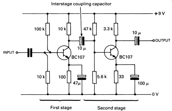
FIG. 7 a two-stage amplifier, using the same circuit configuration
as FIG. 6
2. GAIN OF MULTISTAGE AMPLIFIERS
When calculating the total gain of amplifiers having more than one stage, it is important to realize that the total gain of the system is equal to the gains of each individual stage multiplied together, not added. If the stage gain in a two-stage amplifier were 30, then the total gain of the system would be 30 x 30 = 900.
3. NEGATNE FEEDBACK
Feedback is often applied over more than one stage. FIG. 8 shows a commercially produced design incorporating this feature.
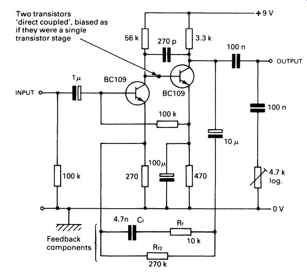
FIG. 8 a commercially produced amplifier, intended for use with
a tape-player; the input is provided by a tape playback head, and the
output is fed to an audio power amplifier (see Section 13)
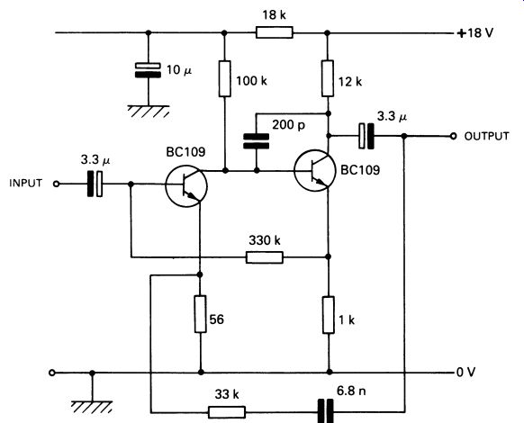
FIG. 9 another tape-player amplifier, using slightly different circuit
techniques; the transistors are directly coupled
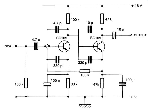
FIG. 10 a third tape-player preamplifier design-there are many
variations on this theme (this circuit is from a commercially produced
tape player).
It is possible to use feedback to alter the frequency characteristics of an amplifier. It is often necessary to limit the high frequency amplification of a system, and this is easily done using a feedback capacitor instead of a resistor. The capacitor's use as a 'frequency sensitive resistor' is clear. At low frequencies, the small value of capacitance feeds back only a tiny proportion of the signal, whereas a progressively larger proportion of the signal is fed back as the signal frequency increases.
In FIG. 8 the feedback line is from the collector of the second transistor to the emitter of the first transistor. It is coupled via a large capacitor (10 uF) so that it does not affect the bias conditions. Frequency selective components in the feedback line establish the frequency response of the amplifier: Cr, Rr and Rr2 are calculated so that this amplifier gives the right frequency response for a tape playback head. The amplifier was designed for a high-quality tape-player.
The 270 pF capacitor between the two transistor collectors operates to limit the high frequency response of the amplifier, and the variable resistor across the output, in series with a capacitor, trims the overall frequency to suit the amplifier that follows.
There are many variations in amplifier design, though there is a basic similarity between types, as one might expect. Figures 10.9 and 10.10 illustrate two more commercially produced designs-another two tape player preamplifiers.
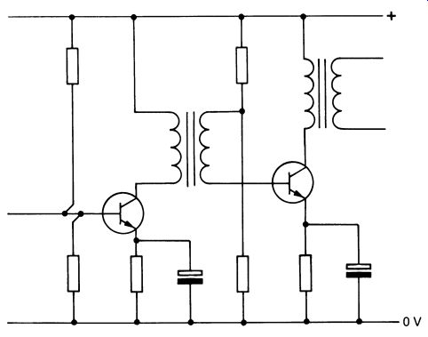
FIG. 11 a two-stage amplifier using transformer coupling between
stages and at the output (transformer coupling is now little used)
4. TRANSFORMER COUPLING
Transistor stages are generally coupled with capacitors, as in the preceding three circuits, but they can also be coupled with transformers. Originally this was the preferred method, but as components and circuit design have improved transformers have been used less and less.
The resistance of the transformer's primary winding can form the collector load of the first stage of a two-stage amplifier. Transformer coupling is illustrated in FIG. 11. Transformer coupling is not widely used now, mainly because of the size (at least 2 em cube) and the relatively high cost of the transformer.
5. STAGE DECOUPLING
The circuit in FIG. 7 may require a couple of extra components to make it work properly in conjunction with a power amplifier stage. Consider an amplifier that is built into a tape player. The output from a cassette tape head is very small-a few hundred microvolts-but the player's power output into the speaker may be as much as a watt, even for a small portable machine. The amount of amplification is therefore considerable.
Power to drive the speaker has to come from batteries, and under heavy loads the battery voltage will drop. Sudden loud noises on the tape will cause rapid voltage drops.
Inevitably, the voltage changes will be reflected by changes in the low power amplifier's quiescent output voltage, which is stabilized at about half the supply voltage. The variation in voltage of the first stage is duly amplified by the second stage, and a large and completely unwanted signal propagates through the system. The result is instability--the amplifier oscillates at a low frequency, often with a characteristic sound called, for obvious reasons, 'motor-boating'. The cure is to prevent the rapid changes in voltage supplied to the first stage of amplification. This, fortunately, is easily arranged. The circuit is shown in FIG. 12. Capacitor Cct charges up through Rct until the voltage across it is almost equal to the supply voltage. The values of Cct and Rd are typical for a small-signal audio amplifier. Because the first amplifier stage is concerned with small signals and has small power requirements, Rd does not have to pass a large current and the voltage dropped across Rd is small--only about 0.5 V with a 1 mA drain.
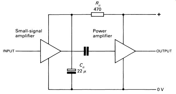
FIG. 12 power-supply decoupling
Imagine a powerful transient -perhaps a bass drum -<:a using a momentary voltage drop of 1 V in the power supply to the system. Neglecting for a moment the current drain of the first stage, Cct has about 0.5 V higher potential across it than the supply voltage, but cannot discharge immediately. It can only do so via Rd, at an initial rate of about 1 mA (by Ohm's Law), which rapidly decreases as the potential by which the capacitor exceeds the supply voltage diminishes. Adding the amplifier's current drain, it is nevertheless quite a long time--in electronics terms-before the supply to the first stage drops enough to affect the output.
Protected against sudden changes in supply voltage to the low-power stages, an amplifier is much more stable. Power-supply decoupling is a feature of almost all amplifier designs which have a large power output and large overall gain. Exceptions to this are to be found in integrated circuit amplifiers; the need for stabilization of the power fed to the early stages still exists, but is fulfilled by more sophisticated voltage regulator systems.
6. INPUT IMPEDANCE
The input impedance of an amplifier is the ratio of the input voltage to input current-it is expressed in ohms, and can be thought of a being similar to resistance, but applicable to alternating as well as direct voltages and currents. The input impedance of an amplifier is an important parameter, and is considered when the amplifier is connected to an external signal source-such as a record-player pick-up or tape head.
A cheap record-player might well use a crystal pick-up cartridge (see Section 13) which generates a relatively high voltage output signal--as much as a volt-but has a very high internal resistance. FIG. 13a shows the cartridge connected to an amplifier. If the cartridge has an internal resistance of 5 Mil--a typical value--and the amplifier has an input impedance of 2500 n, then the total current flowing in the input circuit, FIG. 13b will be I= V/R I= 1/5002500 I= 0.2 uA and of the total 1 V, only 2500/5 000 000, or about 0.5 mV, will be avail able to the amplifier.
FIG. 13 (a) a record-player pick-up, connected to an amplifier; the impedance 'seen' by the pick-up affects the efficiency with which power is transferred from the pick-up to the amplifier (b) a high impedance (crystal) pick-up feeding into a low impedance amplifier is not very efficient.
An amplifier with a higher input impedance should therefore be used, to maximize the efficiency and make best use of the high output voltage of the crystal pick-up. Conveniently, a FET can be used, since the FET has a very high input resistance. A commercial circuit using a JUGFET is given in FIG. 14a. The input impedance is about 5 M-Ohm.
A more usual alternative is to use a configuration of two bipolar transistors known as a Darlington pair. The basic connections are shown in FIG. 14b, and a commercial amplifier (easier to follow than the one in FIG. 14a!) is given in FIG. 14c.
This particular circuit is an interesting one. The two transistors of the Darlington pair give a high input impedance, and this stage is capacitor coupled to the second stage-note that it is un-stabilized! A feedback capacitor (20 nF) is used to control the frequency response. The design is simple and is suitable for a wide range of small-signal applications; it was used as a tape reader preamplifier, but could form the basis of an interesting construction project.
FIG. 14 (a) a commercially designed amplifier using a FET to provide a very high input impedance (b) a Darlington pair of transistors provides high input impedance and considerable gain (c) another commercially designed circuit, using a Darlington pair at the input.
7. OSCILLATORS
It is often necessary to generate a continuously changing voltage or current.
The frequency of change depends on the applications, but could be any thing from one cycle in several minutes to hundreds of megahertz. A circuit that generates such a signal is known as an oscillator. About the simplest is the relaxation oscillator, demonstrated in the circuit in Figure 1 0.15a.
This rather old-fashioned circuit makes a good demonstration because you can see it working! It uses a neon lamp. The neon lamp is filled with neon gas at low pressure. When sufficiently high voltage is applied to the lamp terminals, the neon gas begins to conduct electricity, and at the same time glows red. The lamp will continue to conduct (and glow) until the voltage drops to a level rather lower than that required to 'strike' the neon. It is important to notice that the voltage required to initiate conduction is higher than the voltage required to keep the lamp on.
When the circuit is connected to a voltage source as shown (a high voltage battery, for example) the capacitor C is uncharged. It slowly charges up via resistor R, and the voltage across it increases. At the point where the voltage across the capacitor (and, of course, across the neon lamp terminals) reaches the striking voltage of the neon, the lamp abruptly turns on.

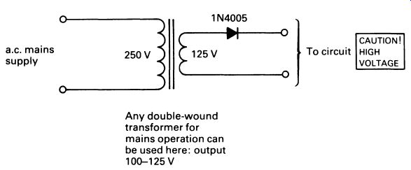
FIG. 15 (a) a simple oscillator, using a neon lamp and capacitor
(b) a suitable power supply for the circuit in FIG. 15a; the diode
must have a working voltage of at least 200 V.
Current from the capacitor now flows through the lamp, which rapidly discharges the capacitor until the voltage across it drops below the level required to sustain the lamp. The lamp goes out and the cycle repeats.
The circuit shown in FIG. 15a is useful for demonstrations, but requires a d.c. power source of about 150 V. A suitable power supply is shown in FIG. 15b. For safety, this circuit should not be used direct from a.c. mains. This illustrates the main reason that the neon oscillator is little used-modern circuits tend to be low voltage. Also, the frequency of oscillation is subject to all sorts of variables; supply voltage, temperature, and even the amount of light falling on the neon lamp will change the frequency.
8. THE BISTABLE MULTIVIBRATOR
A circuit which can assume two stable states is known as a bistable circuit.
Such a circuit is illustrated in FIG. 16. Essentially, it consists of two simple transistor amplifier circuits, connected so that each transistor's base is connected, through a resistor, to the collector of the other.
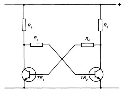
FIG. 16 a bistable multivibrator circuit
If TR 1 is conducting, its collector will be only a 0.7V or so above OV, and TR2 is therefore switched off; it is in the non-conducting state. TR 2 , in contrast, has its collector at a voltage approaching that of the supply.
TR 1 base is therefore held at a high potential which keeps it on. The circuit is clearly stable in this configuration, and remains with TR 1 on and TR 2 off indefinitely.
The circuit is, however, symmetrical, and can equally well be stable with TR1 off and TR2 on.
Bistable circuits like this form the basis of many sorts of digital memory elements, as we shall see in Section 21.
9. THE ASTABLE MULTIVIBRA TOR
Next, look at FIG. 17. Assume TR 1 is on; it can only hold the base of TR 2 at a low potential until C1 is fully charged. RB2 now turns TR 2 on, and the voltage applied to the base of TR 1 drops. It helps to think of RB1, C2 , and the collector-emitter junction of TR2 , and to consider the changes in potential of the various points in the circuit when the capacitor is charged and uncharged, and TR2 on or off. See FIG. 18. TR1 turns off and the circuit assumes the second 'stable' state. But only until C2 charges up. Then the circuit swaps over again, TR1 coming on the TR2 turning off. This circuit will continue to switch back and forth between the two states at a rate controlled by the circuit values.
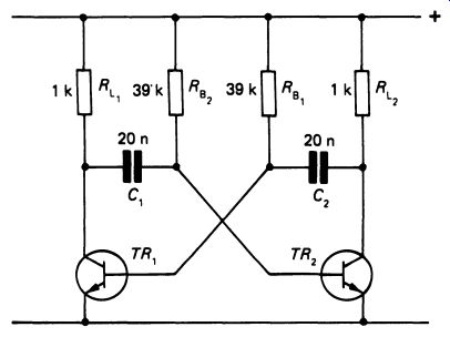
FIG. 17 an astable multivibrator
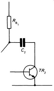
FIG. 18 one 'leg' of the astable
multivibrator.
The low frequency limit is generally the size and leakage current of the capacitor, and the high frequency is limited by the type of transistor used.
The circuit shown oscillates at around 1 kHz--an oscilloscope, high impedance earphone, or even a small speaker in series with a resistor, will soon show it working.
FIG. 19 compares the waveform of the neon oscillator and the astable multivibrator circuits. There are many other types of oscillator circuit in use, though the astable multivibrator is the most common. In digital circuits it is by far the most useful type, as its squarewave output is suitable for driving logic and counting circuits.
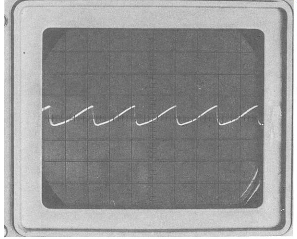
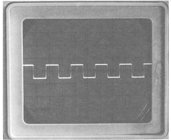
FIG. 19 (a) the waveform produced by the relaxation oscillator in
figure 10.15 (b) the waveform produced by the astable multivibrator
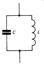
FIG. 20 a simple LC circuit
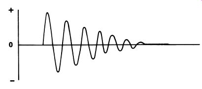
FIG. 21 voltage across the LC circuit after it is energized; note
that although the amplitude of the waveform decays to nothing, the frequency
remains constant
10. LC OSCILLATORS
FIG. 20 illustrates a simple circuit consisting of a capacitor (C) and an inductor (L ). If a direct voltage power supply is connected to the circuit as shown, the capacitor will charge up, but little current will flow through the inductor (see Section 3), at least at the instant of connecting the supply. If the power supply is immediately disconnected, energy will be stored in the capacitor.
The capacitor now discharges into the inductor, and the energy stored in the capacitor is converted into the magnetic field associated with the inductor. After a time, the capacitor will be discharged, and the current flow will stop. But with nothing to sustain it, the magnetic field will begin to collapse, converting its energy back into electricity and recharging the capacitor! While this is happening, current flows round the circuit in the opposite direction.
With the capacitor charged again, the circuit is back in its original state, except that a small amount of energy will have been lost, ultimately radiated by the inductor as a tiny amount of heat. The cycle of charge discharge repeats continuously until all the energy has been lost. FIG. 21 gives a graph of current flowing through the circuit.
Notice that the frequency of oscillation is constant. Every combination of inductor (L) and capacitor (C) has its own resonant frequency, in the same way that a clock pendulum has a resonant frequency. Altering either factor (the length of the pendulum or the weight of the bob) alters the rate of oscillation.
The resonant frequency of the LC oscillator can be calculated as follows:
f= 1 / 2 pi __/ LC
(where f is the frequency in Hz).
It is possible to use the natural resonance of LC circuits to make an oscillator that has a very stable frequency, and usually a sinewave output.
The requirement for oscillation is some form of positive feedback, applied at the resonant frequency by the LC circuit. Several designs are routinely used to achieve this. FIG. 22 shows one of these, the Hartley oscillator.
The 100 nF capacitor provides the necessary feedback, while LC controls the frequency. This circuit needs an inductor that has a tapped winding, i.e. a connection made to the coil in the center as well as to the ends. Otherwise, it is a simple and reliable circuit. The values shown on the circuit are suitable for an audio oscillator--L and C should be chosen to give a frequency of 1-10kHz, if you wish to make up a demonstration circuit.
Another LC oscillator circuit is the Colpitts oscillator. This does not require a tapped inductor. A typical circuit--again, with values for audio frequency operation-is shown in FIG. 23. The equivalent of the center tap is provided by the two capacitors, C1 and C2 , which (in series combination) give the 'C' part of LC. The coupling capacitor, 10uF in this circuit, should be large in relation to c1 and c2, so as not to influence the frequency.
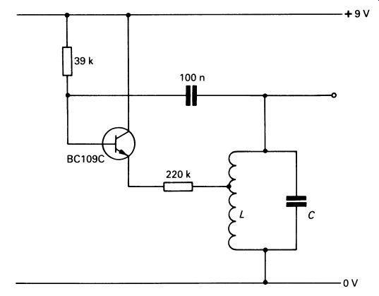
FIG. 22 a Hartley oscillator
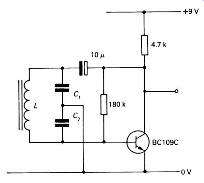
FIG. 23 a Colpitts oscillator, used in place of the Hartley oscillator
where it is not practical to have a tapped inductor
The circuit shown is for operation at audio frequencies; the combined value of C1 and C2 should not be more than 100 nF or so.
11 CRYSTAL CONTROLLED OSCILLATORS
Although LC oscillators can be made quite stable, the frequency of operation is affected to some extent by temperature and voltage fluctuations.
Both the capacitor's capacitance and the inductor's inductance are altered by temperature changes, for example.
The search for a really stable oscillator led to the development of the quartz crystal oscillator. Central to this is a specialized component, the quartz crystal. When a crystal of quartz is subjected to an electric voltage, it flexes. Conversely, when you bend the crystal, a small electrical voltage is generated across the crystal. This direct conversion of mechanical to electrical energy (and vice versa) is known as the piezo-electric effect.
Crystal pick-ups for record players make use of the principle.
Quartz makes a very suitable material for an oscillator crystal because it is elastic-like the pendulum, it takes a long time to stop oscillating once it has started. When 'ringing' at its resonant frequency, the quartz crystal is very like the LC circuit. Energy goes in, which flexes the crystal; the crystal 'swings' back, and electrical energy is produced; as it 'swings' back the other way, the voltage is reversed, and a graph of its output voltage would look just like the one in FIG. 21.
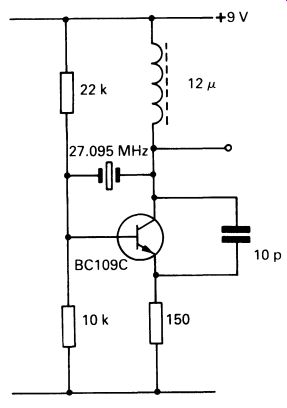
FIG. 24 for extreme frequency stability, a quartz crystal controlled
oscillator is used.
A typical crystal oscillator is illustrated in FIG. 24. This one works at radio frequencies, in the h.f. band--see Section 15. The crystal itself provides the necessary feedback between the collector and base of the transistor. Note the use of the inductor in the collector line. This has a low d.c. resistance for the correct biasing levels, but has a high resistance at radio frequencies and allows the output to be taken between the collector and positive supply line. The circuit can be made to oscillate at a frequency determined only by the crystal, regardless of the precise values of other circuit components.
Quartz crystals can be made cheaply and accurately, and in suitable circuits can give astoundingly accurate control. This type of oscillator is used in digital watches, and an accuracy of ten seconds a month (within the reach of the cheapest digital watch) implies a long-term oscillator stability of better than 1 part in a -! million. Quartz crystals can be made to work over a range of frequencies from tens of kHz to a few MHz.
12. POWER SUPPLY REGULATORS
In Section 7, the Zener diode was mentioned as a component that is useful for providing a reference voltage. Many circuits require a very stable supply voltage, and the Zener diode is generally used in this context. The simplest possible circuit is given in FIG. 25.
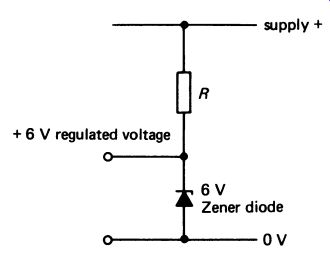
FIG. 25 a simple Zener diode voltage regulator The disadvantage
of this is the fact that all the current for the load is supplied through
resistor R. The value of this resistor is determined by the power dissipation
of the Zener diode, since with the load disconnected all the current
flowing through the resistor also flows through the diode. This circuit
is therefore limited to applications where very small currents are involved.
A more useful circuit is given in FIG. 26.
This uses a bipolar transistor to carry the load current, and also to amplify the regulating effect of the Zener diode to provide more accurate regulation. Operation of the circuit is as follows. If there is no load, no current flows through the collector-emitter junction of the transistor. The only current is that flowing through the resistor and the diode, just a few milliamps.
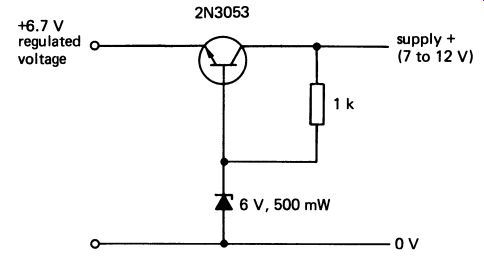
FIG. 26 a voltage regulator providing improved regulation and increased
output current compared with the circuit in FIG. 25
When a load is connected, current flows through the transistor, since the base is held at (in this case) 6 volts, which biases the transistor into conduction. All the while the voltage at the emitter is at or below 6.7 volts (allowing for the voltage drop across the transistor junction) the transistor remains forward biased. But the voltage at the emitter can never rise above 6 volts, since this would involve a higher voltage on the emitter than on the base, reverse-biasing the junction and causing the transistor to switch off. In practice, the voltage on the emitter rises to about 6.7 volts and stays there. If the input voltage to the regulator changes, this does not affect the regulated voltage unless, of course, the input voltage drops below 6.7 volts.
Similarly, changes in the resistance of the load will result only in a compensating change in the bias conditions of the transistor, the voltage at the emitter remaining substantially constant. This type of regulator is useful and inexpensive. The output current is limited by the current and power rating of the transistor.
It is convenient to fit the whole of the regulator circuitry on an integrated circuit, and such components are available cheaply. FIG. 27 shows a 5-volt regulator circuit, capable of handling currents up to 1 amp.
The performance of the IC is considerably superior to that of the circuit in FIG. 26, with more accurate regulation, short-circuit protection and automatic shut-down in the event of the IC overheating.
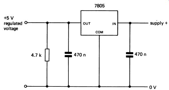
FIG. 27 a high performance 5-volt regulator using an integrated
circuit
Voltage regulator designs are many and varied, but these days most are based on ICs. High-performance versions use switch-mode regulation, in which the voltage source is switched on and off at a high frequency, the ratio of 'on' to 'off' (the mark-space ratio) changing according to the demands of the load. Such regulators are much more complex, but are more efficient in that little waste heat is produced.
QUESTIONS
1. Why is a bias resistor (or network) required for even the simplest audio amplifier using a single transistor?
2. Why is a capacitor commonly used to couple stages of a multistage transistor amplifier?
3. If an amplifier has a voltage gain of 20 per stage, and it has three stages, what output signal will result from an input of 150 uV?
4. Which types of oscillator give the best frequency stability?
5. What kind of output waveform is obtained from (i) an astable multi vibrator, (ii) a relaxation oscillator, (iii) an LC oscillator?