AMAZON multi-meters discounts AMAZON oscilloscope discounts
7-1. High-Frequency Response Limitations of Service-Type Scopes
The carrier frequencies of some of the test signals that it is desirable to display on a scope during visual sweep alignment and troubleshooting of the r-f, i-f, and video amplifier sections of tv receivers, are far too high to permit the conventional medium-cost service-type scope to display them directly. For example, the r-f alignment of vhf tuners may involve the use of sweep carrier frequencies in excess of 200 mhz; of video i-f amplifiers, sweep carrier frequencies of approximately 20 to 50 mhz; of video amplifiers, to 4 or 4.5 mhz.
The majority of such present-day service-type scopes combine a relatively high deflection sensitivity (sensitivity through vertical amplifier approx. 0.01 to 0.02 volts rms per inch of deflection), whid1 is required in practical r-f stage alignment work, with a somewhat limited vertical-amplifier frequency response that usually does not exceed 1 or 2 mhz at the -3 db point. However, for some purposes most of these types of scopes are useful for frequencies somewhat be yond the ones just mentioned because their frequency-response characteristic falls off gradually. More costly wide-band scopes, which have a frequency response to 4.5 mhz (or somewhat higher) at the -3 db point, and are usable at frequencies somewhat beyond this, are available. However, it will be found that the deflection sensitivity of such scopes is generally only 30 to 50 percent of that of the scopes referred to above, usually being of the order of approximately 0.011 or 0.04 volts rms per inch. This reduces their usefulness somewhat in some types of tests, for example in the alignment of r-f amplifier stages where a low signal level exists.
An answer to this problem is provided in the dual-band type of scope which provides dual bandwidth and dual sensitivity suitable for all tv servicing requirements. The specifications of a typical service type scope of this kind are as follows: Wide Band: Frequency response flat, within -I db, from 3 hz to 4.5 mhz, with direct sensitivity of 0.035 volt rms per inch.
Narrow Band: Frequency response flat, within -3 db, from 3 hz to 500 khz, with direct sensitivity of 0.0035 volt rms per inch.
Such a scope is even suitable for checking the 3.58-mhz color sync burst and the 3.58-mhz oscillator signals in color tv receivers.
It is well known that a scope can be used at very much higher frequencies than those defined by the frequency-response characteristic of its vertical-deflection amplifier, provided that the signal voltage is applied directly to the deflecting plates of its cathode-ray tube. In fact, many scopes are arranged so that this can be easily accomplished by opening a jumper provided on the scope terminal board (or in the rear) which ordinarily connects the scope vertical amplifier to the vertical deflection plates. Service technicians often take advantage of this feature when it is necessary to make careful analyses of the equalizing pulses and the vertical pulses, or the fine detail of the horizontal sync pulse, with a scope whose vertical-amplifier frequency response is inadequate. However, in most testing and circuit-alignment procedures that involve the higher frequencies, the available voltage is not sufficient to obtain a deflection that is large enough to be useful when direct connection to the deflecting plates is resorted to, because the deflection sensitivity for this mode of operation is very low, being of the order of approximately 12 volts rms per inch in 5-inch scopes, and 24 volts rms per inch for the 7-inch size.
7-2. Function of Demodulator Probes
If the high-frequency voltage that is to be displayed happens to be modulated, as is usually the case, it is unnecessary to have the scope display a complete trace of each individual cycle of the high-frequency carrier. If the modulated high-frequency signal is first demodulated (detected), and the modulation voltage which is recovered in the process is applied to the scope input terminals, the scope will display a trace of the modulation envelope. Fortunately, this hap pens to be the waveform that is usually of interest to the service technician in his work. Since most of the modulation frequencies encountered in tv receiver operation and test work are comparatively low, and within the normal response ranges of the vertical amplifiers of conventional service-type scopes, the modulation voltage may be applied to the input of the vertical amplifier of the scope, and advantage may be taken of the gain provided by this amplifier. Thus, the demodulator makes possible effective testing in high-frequency circuits which would otherwise be closed to a conventional service scope.
--------------
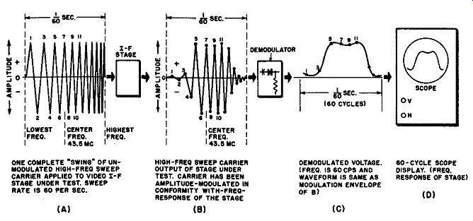
7-1. Operational steps in the functioning of a demodulator probe when employed to ascertain the frequency-response characteristic of a circuit to which is applied a test sweep-signal of too high a carrier frequency to be applied directly to the scope. The demodulator accepts the modulated carrier-frequency output of the circuit under test, demodulates it, and delivers the low-frequency modulation envelope as a voltage to the vertical amplifier of the scope which displays it. In the example illustrated here, the scope can display the 60-cycle output from the demodulator, although it is unable to reproduce the 43.5-mhz carrier output from the circuit under test. ----
---------------
To illustrate the typical actions which take place in an arrangement of this kind, consider the example illustrated in Fig. 7-1. The constant-amplitude sweep signal (Fig. 7-1A) having a center carrier frequency of 43.5 mhz, with 5-mhz deviation and a 60- hz sweep rate, is applied to the input of a video i-f amplifier stage for the purpose of checking and adjusting its response characteristic by the visual alignment method. The sweep signal which appears at the output circuit of the stage is shown in part B of the figure. Observe that it is amplitude-modulated in conformity with the response characteristic of the stage under test. Since the carrier frequency of this signal has much too high a frequency for passage through the vertical amplifier of a scope, we must demodulate it. The waveform of the demodulator output voltage, shown in Fig. 7-1C, is substantially the same as that of the envelope of the high-frequency carrier at the i-f stage output. This waveform represents the frequency response of the stage. Since the frequency shown in Fig. 7-C is only 60 hz, it may be applied to the vertical amplifier of the scope, and a trace of this voltage, (that is, a trace of the frequency response of the stage) will be displayed on the screen.
In some of the alignment and test procedures where this problem is en countered, one of the detectors (demodulators) of the receiver happens to be conveniently located at the output of the circuit under test, in which case it may be used to perform the required demodulation. For example, if the response characteristic of the last video i-f stage, or of this stage together with others preceding it, is being checked, the video detector which follows it may be used to perform the required demodulation of the test signal. In this case, the test signal is taken off at the output circuit of this detector, and applied to the scope. However, such a detector is not always conveniently present at the output of the circuit under test. For example, if the frequency response of one of the earlier video i-f stages, or of the video amplifier, is being checked, there is no receiver detector immediately following it. In such cases, an external demodulator must usually be used ahead of the scope input terminals if the scope being employed does not have a frequency-response characteristic that is practically flat out to the carrier frequency of the test signal being employed. In order to apply this demodulator as close as possible to the high-frequency signal take-off point in the receiver, it is usually constructed in probe form.
It may be noted in passing that there are some scopes in use which have a built-in demodulator which may be switched into the input circuit of the vertical amplifier when desired. However, since a shielded test cable having a rather substantial capacitance must then be used between the demodulator input and the point of test, successful demodulation with this arrangement is limited to signals of relatively low-frequency, The majority of service technicians prefer to use external demodulator probes which may be applied directly at the point of test, since the input capacitance of the demodulator, which is applied across the circuit under test, is thereby greatly lessened.
Demodulator probes are usually built around crystal-diode rectifiers, because the crystal diode possesses desirable features such as:
(1) compactness; (2) good frequency response to as high as 250 mhz or more; (3) no heater involved, so a possible source of hum as well as heater wiring and heater voltage source are eliminated; (4) operation far above ground potential is possible; and (5) it has an input voltage rating that is sufficiently high for most of the ordinary applications of such probes. The crystal diodes used must be types that not only have a relatively high front-to-back resistance ratio, but are also able to accommodate reasonably high a-c signal voltages without loss of sensitivity or burn-out. The 1N34, 1N34-A and 1N48 crystal diodes are types widely used in such probes.
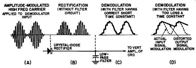
Fig. 7-2. Principle of operation of the diode demodulator, and effect of the
time constant of the filter circuit on the waveform of its output voltage.
7-3. Basic Time Constant Requirements of the Demodulator Probe
A diode demodulator consists essentially of a diode rectifier associated with a load resistor and filter circuit. The time constant of the filter must be chosen to be sufficiently long so that the carrier-frequency variations in the output voltage are filtered out, but not long enough to filter out the lower-frequency variations which represent the modulation. Thus, it is evident that the essential difference between a demodulator probe, and the vtvm rectifying probes discussed in Section 6, is that a demodulator probe is designed to have a short time constant as compared with that of a rectifying probe, insofar as the signal to be ob-served or measured is concerned. Perhaps this may be better understood by comparing the illustrations in Fig. 6-5C, Fig. 6-6C, and Fig. 6-7C, with those in Fig. 7-2 which summarizes the action of a demodulator in some detail. Illustration D in Fig. 7-2 shows that the demodulator output actually consists of a low-frequency component superimposed on a d-c component.
Thus, a rectifying probe for use with a vtvm is designed to have a comparatively long time constant, so that it will deliver a smooth d-c output proportional to the peak (or peak-to-peak) amplitude of the carrier wave. A demodulator probe for use with a scope is designed to have a long time constant with regard to the carrier wave, but a short time constant with regard to the modulating wave so that it will deliver a d-c output which retains the low-frequency fluctuations which constitute the amplitude-modulation of the high-frequency carrier wave.
The time constant of the filtering circuit of a demodulator probe must fall within a suitable range for the rate of change of the modulation envelope that will be encountered in the application in which the probe is to be used. otherwise, a distorted response trace will be obtained on the scope. If the probe time constant is too short, the output waveform will tend to follow the high-frequency carrier wave rather than the envelope. Also, the shape of the scope trace for falls in the modulation envelope will be correct, but it will be incorrect for rises in the modulation envelope. If the time constant is too long, even the modulation envelope tends to be smoothed out. Under these conditions, the shape of the scope trace for rises in the modulation envelope will be correct, but the trace will be incorrect for falls in the modulation envelope (see Fig. 7-2D). A simple method of checking the suitability of the time constant of a de modulator probe for use with an intended test-signal is explained in Sec. 7-18.
7-4. The Series-Rectifier Type Demodulator Probe
The series rectifier, the shunt rectifier, and the voltage-doubler rectifier, whose operation is discussed in Section 6, are the basic circuit arrangements employed in demodulator probes. Several variations of these are employed for specialized applications. All of them will be reviewed here, with particular emphasis placed on both the desirable and the undesirable characteristics of each that may determine its suitability for specific intended applications in tv service work.
(1) Simplified Form of Series-Rectifier Probe, and its Action. The series rectifier demodulator utilizes a crystal-diode rectifier in series with the input circuit. It is inherently more sensitive than the shunt demodulator arrangement.
As shown in Fig. 7-3A, the simplest possible probe of this type consists of a crystal diode feeding into the capacitance, C, of a shielded test cable.
The capacitance of the shielded test cable together with the input capacitance of the scope, is equivalent to a shunt capacitance C having a value of approximately 75 to 100 µµf for typical service-type scopes. The crystal diode charges this capacitance as the modulation envelope rises (see enlarged detailed view in Fig. 7-2C), and little distortion is encountered in this portion of the operating cycle. Next, as the modulation envelope falls, the charged capacitance...
Fig. 7-3. (A) The simplest, and also the most sensitive arrangement for a
conventional crystal-diode demodulator probe consists of utilizing the crystal
diode as a series rectifier whose output charges the capacitance, C, of the
shielded cable. (B) A bleeder resistor, R, is added to reduce the time constant
of the circuit sufficiently so that effective demodulation is obtained. ( C)
A series isolation resistor R1 is added to provide further r-f filtering in
order to remove the sawtooth ripple from the output voltage and thereby minimize
possible erratic frequency response characteristics caused by resonance and
anti-resonance effects in the cable.
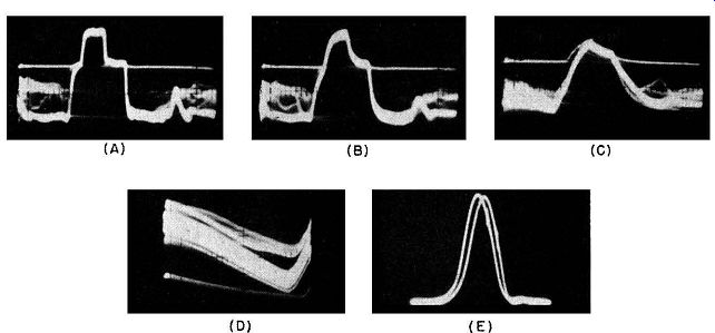
Fig. 7-4. Effects of the use of an excessively large value of isolating resistance
in a demodulator probe. Progressively increased waveform distortion to which
horizontal sync pulse (A) is subjected as the value of isolating resistance
R1 is increased (B), increased more (C), and increased still more (D). Use
of an excessively large isolating resistor also causes vertical displacement
of the position of a marker used on the steep side of a response curve, as
shown in (E). The two response traces shown here were made with different values
of isolating resistor in the probe. Observe the shift in the vertical position
of the marker.
...can discharge only through the back-resistance of the crystal and through the voltage-source resistance. If the crystal is in good condition (has a substantial front-to-back resistance ratio), and no bleeder resistor is provided, capacitance C tends to hold its charge as the modulation envelope drops. In practice, C will not hold its charge indefinitely because the crystal diode has a back resistance of approximately 100,000 ohms, and C discharges slowly through this back resistance and the resistance of the voltage source. (If the scope input circuit is not provided with a d-c blocking capacitor, this circuit draws some discharge current also.) However, the waveform distortion usually encountered in conventional tv test work with an arrangement of this kind is considerable, as negative-peak clipping results from the long discharge time-constant which results. Also, like any oversimplified device, such a demodulator is normally subject to several objectionable operating characteristics, such as output-waveform distortion, relatively high hum-voltage conduction, and susceptibility to shift of rectifier operating point due to a bias voltage developed by possible d-c leakage through the scope input blocking capacitor.
To overcome the negative-peak clipping condition in service applications, a bleeder resistor, R, is usually connected across the circuit, as shown in Fig. 7-2B. This resistor allows the charge to dissipate at a faster rate, thus decreasing the time constant of the filter circuit sufficiently so that the output voltage will definitely follow the low-frequency modulation envelope of the applied high frequency carrier voltage (see Fig. 7-2). However, it should be remembered that a crystal diode which has a low value of back resistance may not require a bleeder, and will cause a demodulator probe to have low sensitivity if a bleeder is used.
Figure 7-2C shows the demodulation action in detail. The rectifier charges up the capacitor to the peak voltage of the high-frequency carrier cycle, and the bleeder immediately starts to discharge the capacitor; however, the charge does not fall far before the next carrier cycle peak appears and brings the charge up to that peak voltage. The output voltage thus has the shape of the modulation envelope, with a sawtooth ripple present. This ripple appears because the bleeder always discharges the capacitor a little faster than the rate of change of the envelope (at least in the normal operation of the probe.) The important consideration is that the bleeder must discharge the capacitor fast enough between successive carrier peaks to allow the output to drop as fast as any envelope drop which may occur. However, if the bleeder resistance is too small, the probe will be insensitive.
(2) Probe-Cable Resonances and Use and Effect of the Isolating Resistor.
Sawtooth ripples present in the demodulated output of any form of demodulator probe represent r-f variations which can lead to serious disturbances in the operation of the probe at the higher r-f and i-f carrier frequencies, depending on whether the shielded-cable length happens to be an odd, or even multiple of ¼ of the operating wavelength. Resonances and anti-resonances may occur in the probe cable at certain frequencies; see Sec. 3-2. These cause the probe to have abnormal output (increased sensitivity) at certain carrier frequencies and de creased output (subnormal sensitivity) at other frequencies. In severe cases, the output may be practically zero at some carrier frequencies, while at others the output may be several times the voltage of the input. The probe is not generally useful above frequencies at which the resonant characteristic of the cable begin to affect the output to the scope. Consequently, it should be designed so that such abnormalities in frequency response do not occur within the carrier-frequency range over which it is intended to be used.
The sawtooth ripple variations may be removed by providing a suitable low-pass filter in the output network. Addition of isolating resistor R1 in Fig. 7-3C may provide such a filter, with the test-cable capacitance C acting as the shunting capacitor. This filter isolates the shielded cable (and the scope) from the high-frequency circuit of the probe. The constants of the filter must be selected to provide adequate carrier-frequency filtering action, but not too much.
If the filtering is excessive (time constant too long), a 60-cycle square-wave modulation envelope, for example, will be distorted. It will be shown later (see Sec. 7-8) that a demodulator probe used for tv circuit-alignment work must be able to pass a 60-cycle square-wave envelope essentially without distortion. De modulator probes distort the modulation waveform increasingly as the modulation frequency increases. This is illustrated later.
The effect of the increase of isolating-resistance value upon the waveform distortion produced in the output of a demodulator probe is shown in parts A to D of Fig. 7-4, for a horizontal sync pulse.
Another effect of using an excessively large isolating resistance is that it may cause a vertical shift in the position of any frequency markers that are used on the steep side of the demodulated response curve, as shown in Fig. 7-4E. The displacement results because it then takes too long a time for the cable input capacitance to charge and discharge through the excessively large isolating resistance.
The cable resonance problem may also be attacked by the use of suitably low values of shunt resistance across the cable input to damp or "swamp" out the resonant response of the cable, but of course this decreases the probe sensitivity. Another possibility is the use of a shunt capacitor instead of a series isolating resistor.
Better waveform reproduction and greater sensitivity are obtained from a series-type demodulator probe by omitting the isolating (or shunt swamping) resistor. However, the improvement in waveform and sensitivity is obtained at the expense of a reduced carrier-frequency range, since the probe is then not useful above frequencies at which the resonant characteristics of the scope input cable begin to affect the operation of the probe. If greater sensitivity is required, it is usually a better practice to use a suitable audio-frequency pre-amplifier between the probe output and the scope input terminals to obtain the required overall sensitivity. This may be a conventional audio amplifier which has a low hum level, since the frequency range of the modulation waveform is usually relatively limited.
(8) The D-C Blocking Capacitor. Most scopes are provided with a d-c blocking capacitor, C2, in series with the input circuit, as shown in Fig. 7-5. When this capacitor is present in the scope, its quality and operating condition are very important to the operation of a series-type demodulator probe that is to be used with the scope. If the probe tip is applied to the plate terminal of a tube in the tv receiver during a test, a d-c voltage component of the order of 90 to 250 volts or more may be present. The presence of leakage resistance, R3, in this blocking capacitor will cause any d-c voltage applied to the probe tip to produce a direct-current flow to ground through the continuous series circuit provided by the crystal diode, isolation resistor R1, leakage resistance R3, and the input resistance R2 of the scope.
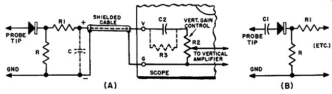
Fig. 7-5. (A) The simplified type of series-crystal demodulator probe appears
very insensitive if the scope input blocking capacitor C2 has appreciable leakage,
represented by R3. A d-c path for the flow of current is then provided through
the crystal diode, R1, and the scope input resistance R2. This produces a bias
across the diode, shifting its operation to a relatively insensitive portion
of the crystal characteristic. This may be prevented by use of a series blocking
capacitor C1 in the probe itself, as shown in (B).
Service scopes receive hard usage, and the blocking capacitor will sometimes be found to be in a defective condition. The flow of de through the crystal diode, which results from a defective blocking capacitor having excessive leakage, produces a voltage drop or bias across the crystal diode, which moves the operating point to a relatively insensitive portion of the crystal characteristic, resulting in reduced sensitivity of the probe. In severe cases, the current may be large enough to damage the crystal. For this reason, a series blocking capacitor C1 is usually included in the series demodulator probe itself, as shown in Fig. 7-5B, although this arrangement is somewhat less sensitive.
(4) Susceptibility to Hum Voltage. Considerable hum voltage exists in many video-amplifier circuits. The hum level may not be sufficient to adversely affect the picture quality of the tv receiver to a noticeable extent, even though it may be high enough to interfere with video-amplifier signal-tracing and adjustment procedures. A demodulator probe that is susceptible to hum voltage is especially troublesome when used in video-amplifier applications.
The series type of demodulator probe will be found to be more susceptible to 60-cycle and 120-cycle a-c hum voltage reproduction than is the shunt type, although use of a small value of capacitance for C1 does afford some relief. This series capacitor is the dominant factor in hum rejection in this type of probe.
In fact, series type probes are designed especially to have fairly good hum-voltage rejection characteristics for use in special applications. These probes differ from the more conventional general-purpose series-type probes only in the low value of series capacitor they employ. Use of shunt resistors in the probe circuit is also often resorted to for reducing the amount of hum voltage which gets through.
In general, the series type demodulator probe is less desirable in video amplifier work than is the shunt type.
7-5. Practical Forms of Series-Type Demodulator Probes
Although the shunt type of demodulator probe provides far greater immunity from hum voltages than does the series type, there are applications, such as in some signal-tracing work, where the series type of probe has greater utility because of its greater sensitivity.
Numerous variations of the simple form of series demodulator probe discussed thus far are possible and are useful in tv service work. Each employs a proper choice of probe constants to achieve useful display of the modulation envelope of the signal to be checked. A probe having a relatively high input impedance is illustrated in Fig. 7-6. No series isolation resistor is employed. The 100,000-ohm shunt resistors greatly reduce the amount of hum voltage which gets through the probe.
Some series-type demodulator probes are purposely designed to have a low input impedance. Those are considered in detail in Sec. 7-10.
7-6. The Shunt-Rectifier Type Demodulator Probe (1) Basic Form of Shunt-Rectifier Probe, and its Action. The shunt-rectifier type of demodulator probe (see Fig. 7-7), which employs a crystal diode in shunt with the input circuit, is inherently less sensitive than the series type but it possesses certain operating advantages which make it more widely used. Its basic circuit operation, insofar as the actions of the rectifier, the series charging capacitor, the load resistor, and the series isolating resistor are concerned, is similar to that of the shunt rectifying probe (see Sec. 6-3 and Sec. 6-14), so this explanation will not be repeated here. Note that the crystal is so polarized as to produce a positive output voltage for the scope. This is in contrast with most rectifying probes for vtvm's, where the probe responds to positive peak input voltages and produces a negative output voltage for the meter. The circuit constants are such that the time constant of its filter circuit is considerably shorter than that employed in the rectifying probe. The time constant is made short enough so that the output voltage follows the modulation envelope of the applied carrier, as illustrated in Fig. 7-2.
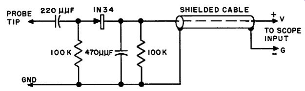
Fig. 7-6. Practical series-type demodulator probe having a relatively high
input impedance and provided with a blocking capacitor, a bleeder resistor,
and a shunting resistor for hum-voltage reduction.
Fig. 7-7. Basic practical form of the shunt-type demodulator probe. The input
capacitance depends upon the mechanical design of the probe, the value of charging
capacitance C1, the value of bleeder resistance R, and to some extent upon
the front-to-back resistance ratio of the crystal diode. The probe input capacitance
varies slightly with the applied in put voltage. Isolating resistance R1 should
be as large as practicable, not only to retain reasonably good 60-cycle de
modulation response, but to isolate all voltages of input carrier frequency
from the cable, so that more uniform high-frequency response free from cable-resonance
effects throughout the rated operating-frequency range of the probe can be
realized. Proper choice of the probe constants must be employed to achieve
a useful display of the modulation envelope on the scope screen, from the modulated
signal employed in the test.
As in other types of probes that employ crystal diodes, the value of the back-resistance of the crystal diode employed determines whether or not a bleeder resistance must be used in the shunt-type demodulator probe. A crystal diode which has a very high value of back resistance may cause a demodulator probe to be unworkable unless a bleeder resistor is provided, as in Fig. 7-6. A crystal diode which has a low value of back resistance does not require a bleeder, and will cause a demodulator probe to have low sensitivity if a bleeder is used.
(2) Probe-Cable Resonances and their Elimination. Since the output wave form of a shunt type demodulator contains sawtooth ripples similar to those in the series-demodulator output, the same cable-resonance possibilities exist (see part 2 in Sec. 7-1). Use of the customary series isolating resistor R1 added to the filter network, or use of suitably low values of shunt resistance across the cable input to "swamp" out its resonance response, are the two methods generally employed to combat this problem. The demodulated waveform is also improved when shunting resistance is used, but, of course some probe sensitivity is sacrificed.
(3) Susceptibility to Hum Voltage. In general, a probe that employs a shunt rectifier (or rectifiers) in combination with relatively low values of series charging capacitance will provide far greater attenuation of 60-cycle and 120-cycle hum voltages, with respect to r-f or i-f voltage$, than does a series-rectifier type probe.
Because of this, it is usually possible to use a shunt-rectifier type probe to develop a video-response curve in a tv receiver whose video amplifier has a relatively high hum level, without perceptible hum interference appearing in the scope trace. This is one of the important advantages of the shunt type of probe in this work. Tests for the presence of spurious voltages in heater circuits, age lines and d-c supply lines are also greatly facilitated.
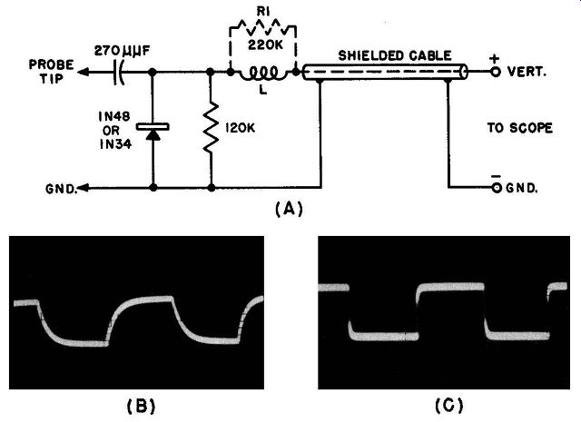
Fig. 7-8. (A) To obtain improved fidelity of the output waveform from a de
modulator probe, an r-f choke L can be utilized in place of (or with) the customary
isolating resistor. A general-purpose probe employing the conventional isolating
resistor only, produced the distorted demodulated output waveform shown in
(B) when a 20-mhz r-f voltage modulated by a 10- khz square wave was applied
to the probe. The improved square-wave output waveform fidelity shown in (C)
resulted when r-f choke isolation was used instead.
7-7. Fidelity of the Output Waveform is Improved by Use of R-F Choke Isolation
When an isolating resistance is employed in a demodulator probe, the output-waveform fidelity for square-wave modulating voltages appreciably above 60 hz, is usually only moderately good. The output-waveform fidelity for higher modulating frequencies may generally be improved substantially, when necessary, by using a video-frequency choke, or a rudimentary filter, in place of the conventional isolating resistor, as shown in Fig. 7-SA. The improvement results from a substantial reduction effected in the time constant of the probe filter circuit.
Choke L may be used alone, or it may be combined with resistor R1, as shown. The choke may be any conveniently available r-f choke selected to provide reasonably high impedance over the carrier-frequency range at which the improvement is to be effected. However, it may have to be selected carefully if "ringing" is encountered in square-wave response. (Among a group of available eligible chokes, the one of highest impedance will be the one which is found to provide maximum deflection on the scope screen over the chosen band of carrier frequencies.) An example of the marked improvement in the fidelity of the output wave form, for a modulating voltage of comparatively high frequency, that is attain able by this method, is illustrated by the results of the rather severe test in parts B and C of Fig. 7-8. More elaborate low-pass filter arrangements can be utilized for this purpose, but the increased complexity of such networks is scarcely justified in service applications.
7-8. Varied Demodulator-Probe Operating Requirements in TV Applications
A general-purpose demodulator probe intended to be used with a scope in tv service applications, unlike a rectifying probe designed for use with a vtvm, is subjected to a variety of operating requirements. For example, when it is used in a sweep-frequency check of a video-amplifier, the probe is called upon to rectify and completely filter all video frequencies from approximately 100 khz to 4.5 mhz, but it must pass a 60-cycle square-wave modulation envelope, essentially undistorted, to the vertical amplifier, of the scope. This calls for a high degree of output-waveform fidelity, and a probe designed to have sufficiently good fidelity will generally have rather low sensitivity. Fortunately, since ample signal voltage is present in the video amplifier, high probe sensitivity is not required for this application.
The input capacitance (or impedance) of the probe also becomes a matter of some importance in this application, for the shape of the response curve will be distorted unless the input capacitance of the probe is approximately the same as the capacitance of the input-grid circuit of the picture tube.
The input capacitance of a crystal probe is determined by its electrical constants and its mechanical construction; that is, the mounting of the probe components with respect to the shielded probe body, value of the blocking capacitor which is used, and the combined effective resistance of the crystal diode and its shunting resistor. These must be suitably related, so that when the socket is removed from the base of the picture tube, and the demodulator probe is contacted to the grid terminal of the socket, the output of the video amplifier will work into substantially the same impedance as if the picture tube were connected.
For use in video i-f amplifier signal tracing, the demodulator probe should have a relatively high input impedance at carrier frequencies from 20 mhz up to 50 mhz. Fidelity of output waveform is not particularly important in this work, and it can be sacrificed to attain the high probe sensitivity usually required for probing a low-level circuit such as the mixer and first i-f stage. Thus, the de modulator probe characteristics most desirable in video i-f amplifier signal tracing are not compatible with those desirable in video-amplifier checking.
For use in testing the flatness of the output of a conventional sweep generator, the probe must have an output which is proportional to signal input at frequencies up to about 220 mhz (and sometimes higher); that is, the probe response must be "flat" over this extremely wide frequency range.
In most cases, good output waveform fidelity from a crystal demodulator probe is obtained at the expense of lowered input impedance. It is never possible to obtain extremely high input impedance to a crystal probe, in view of the operating characteristics of crystal diodes. However, relatively low input impedance is not necessarily a drawback in all uses of a crystal probe, as it is found advantageous to have a low input impedance in certain applications, as in testing the response of a single stage.
A crystal demodulator probe can be designed to provide any one of a number of special operating characteristics that may be desirable in a particular application, such as high input impedance, low input impedance, high sensitivity, excellent output-waveform fidelity, wide carrier-frequency response, etc.
However, it is not possible to combine all of them into a single design of probe.
Use of certain demodulator probes which have special characteristics is often advantageous in service work, and several of the more useful special types are described later in this section. However, each of these is generally useful for not more than a few particular applications.
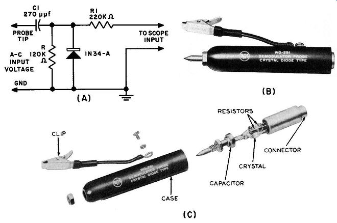
Fig. 7-9. (A) Schematic circuit diagram of a good-quality general-purpose
shunt-rectifier type commercial demodulator probe designed to be especially
useful in tv service work. (B Exterior) view of the probe, which is constructed
in convenient slip-on form. The short ground-return lead and clip are visible
at the top. (C) An exploded view of the probe, showing the compact internal
construction and carefully designed arrangement of the various components to
achieve low input capacitance and wide carrier-frequency response range. Courtesy:
RCA
Since many service technicians do not care to invest in a number of specialized demodulator probes, and prefer to utilize a single probe (or perhaps a couple of probes), for all of their work, commercial demodulator probes generally represent a compromise design in order to meet the greatest number of application requirements in a satisfactory manner even though they may not be perfect. The following characteristics of such a general-purpose demodulator probe should meet the requirements of the application, in the order indicated: (I) input impedance; (2) reproduction of demodulated 60- hz square wave; (3) sensitivity; (4) waveform fidelity (above 60- hz square wave); (5) ruggedness to overload and mechanical shock; and (6) hum suppression. Because of the first and second requirements, most general-purpose crystal probes utilize the basic shunt-rectifier type design shown in Fig. 7-7. Its sensitivity will be found to be moderate, and not equal to that available from the elementary series-rectifier type arrangement shown in Fig. 7-3, but its hum-rejection characteristics are superior. The time constant is designed to be suitable for demodulating carriers which have been modulated by frequencies as low as 60 cycles. Shunt-type probes are generally found most suitable for general signal tracing as well as for video amplifier checking.
7-9. General-Purpose Shunt-Type Demodulator Probes
An example of a practical commercial shunt-type demodulator probe de signed to be useful for a variety of tv servicing applications when modulated carriers are present, is illustrated in Fig. 7-9. The schematic circuit diagram is shown in Fig. 7-9A. The assembled probe, illustrated in part B of the figure, is constructed in a slip-on form designed to fit the standard direct probe and cable supplied with several models of the manufacturer's service type scopes and vtvm's. An exploded view showing the internal construction and component arrangement is illustrated in Fig. 7-9C. The specifications of a demodulator probe of this type are very instructive, and are presented here.
---------------------
SPECIFICATIONS
Frequency Response Characteristics:
RF carrier range _ -500 khz to 250 me
Modulated-signal range ------------· 30 to 5,000 cycles
Input Capacitance (Approx.)-------------------------- 2.25 µµf
Equivalent Input Resistance (Approx.):
At 500 khz ---------
At 1 mhz --------------------------------------- At 5 mhz
----------------------------------- At 10 mhz
-------------------------------- At 50 mhz At 100 me
At 150 mhz
At 200 mhz
Maximum Input: 25,000 ohms 23,000 ohms 21,000 ohms 18,000 ohms 10,000 ohms 5,000 ohms 4,500 ohms 2,500 ohms
\ 20 rms volts A-C voltage
28 peak volts
D-C voltage
250 volts
---------------------
The short time constant filter network in the probe has a rated output frequency (modulation frequency) range of 30 to 5,000 hz. The probe will, there fore, develop the wave envelope of a signal having 60-cycle square-wave modulation, without appreciable distortion. The results of a check on the actual influence of the probe network upon a 1,000-cycle square-wave modulation envelope are presented in Fig. 7-10. It can be seen that although the lower frequencies in the square wave are passed by the probe network, the higher frequencies in it are attenuated somewhat and shifted in phase. However, in tv servicing practice the probe is usually called upon to pass only 60-cycle square waves or equivalent waveforms, so this characteristic is satisfactory and the probe is especially useful
Fig. 7-10. Influence of the filter network of the probe illustrated in Fig. 7-9 upon a 1,000-cycle square-wave modulation envelope. The input to the probe is a 100-mhz carrier, modulated by a 1,000-cycle square wave. The slight rounding of the diagonal comers is caused by the filter network in the output circuit of the probe.
for the observation of sweep-curve response in tv alignment work (in which a 60-cycle sweep is usually employed). The frequency response over the r-f carrier range is rated as essentially flat from 500 khz to 250 mhz, enabling the probe to demodulate any video, video i-f, and tv-channel sweep carriers, or audio amplitude-modulated carriers, within that range. Thus, when used with a sweep generator and an oscilloscope, this probe permits observation of the video i-f amplifier, sound i-f amplifier, video-amplifier, and overall-response curves of a tv receiver. This combination may also be used to obtain the response curves for single stages.
Because the input capacitance of the probe is lower than that of the picture tube, the probe may be connected to the output of the video amplifier with negligible effect on the circuit. The input resistance is satisfactorily high for most service tests.
7-10. Low-Impedance Demodulator Probe for TV I-F Amplifier Work
One of the most useful special-purpose demodulator probes is the low-impedance type, also sometimes called the "traveling detector" because of its particular usefulness as a demodulator in stage-by-stage amplifier alignment and signal-tracing work.
To view the response of a single i-f amplifier stage on a scope when performing stage-by-stage alignment or signal-tracing in the amplifier, the modulated i-f output signal of the stage is usually taken off across the plate circuit of the i-f tube following the stage under test. One difficulty which often presents itself when a typical general-purpose demodulator probe is employed for this purpose is that the input capacitance of the probe may be large enough to cause substantial detuning of the tuned circuit across which it is connected. This detuning may even cause severe regeneration or violent oscillation in some cases. (The subject of probe application in video i-f amplifier work is discussed in greater detail in Sec. 7-29.) One practical solution to this difficulty is to employ a demodulator probe designed especially to have a comparatively low input impedance. This low impedance swamps out the resonant response of a tuned circuit across which it is applied. It has been found in practice that this approach is one of the best answers to problems of circuit disturbance which occasionally vitiate the test by causing oscillation or severe regeneration. It often happens that it is better to swamp out the resonant response of a critical circuit completely, if the response of this circuit is not in question, rather than to partially detune the circuit.
Fig. 7-11. Shop-constructed, low-impedance (traveling detector), series-rectifier type of demodulator probe designed especially for stage-by-stage signal-tracing or alignment work in r-f amplifiers. The output is well filtered by the pi-filter section provided.
The sensitivity of the low-impedance type demodulator probe is less than that of the more conventional medium-impedance and high-impedance probes, so the output voltage is less. However, its sensitivity is usually quite adequate when a sensitive scope is used. If greater output is required, an audio amplifier having suitable response characteristics may be employed between the probe output and the scope input terminals. The advantage of the low-impedance type demodulator probe for this type of application far outweighs its disadvantages.
It does not throw the amplifier into oscillation and, moreover, the display on the scope screen is always the true response of the circuits up to, but not including, the plate circuit across which the probe is applied.
The schematic circuit diagram of a low-impedance series-rectifier type de modulator probe that has good frequency response and is extremely useful in i-f amplifier individual-stage work is illustrated in Fig. 7-11. Since this type of probe is not available commercially, it must be shop-constructed by the technician. It is recommended that the technician should not attempt to enclose a low-impedance probe in a housing if it is to be used for r-f (head-end) applications. However, when used for i-f work it may be enclosed in a suitable metallic case and provided with a flexible ground lead and clip.
One advantage of the circuit shown in Fig. 7-11 is that the charging capacitor acts also as an input blocking capacitor and permits the use of the probe with scopes which may have appreciable d-c leakage in their own blocking capacitor (see Fig. 7-5). The frequency response to carrier-wave frequencies is improved by inclusion of the pi-filter comprising the pair of 0.001-µf capacitors and the 220-ohm series resistor. For reproduction of video waveforms only, this filter may be omitted.
The use of a low-impedance type demodulator probe is specified for individual stage alignment in the service manuals for many tv receivers. In such cases, the circuit constants of the probe used must conform to the receiver manufacturer's recommendations. Otherwise, the demodulated waveform seen on the scope may not have the referenced shape even when the circuit is properly aligned. Six different designs for shop-constructed low and medium impedance demodulator probes recommended for i-f work in the servicing instructions of six tv receiver manufacturers are presented in Fig. 7-12. Some are series type probes; the others are of the shunt type. All are arranged to produce a positive output voltage for the scope.
In the absence of a low-impedance demodulator probe, or in the absence of specific receiver manufacturers' instructions for the construction and use of one, the technician may generally employ his general-purpose high-impedance de modulator probe for such work. If no indication is obtained at a test point in the i-f amplifier, and if oscillation is suspected, a 200- or a 300-ohm damping resistor and a blocking capacitor may be shunted across its input terminals to shunt down and flatten the response of the tuned plate-circuit load to which the scope is applied. This is illustrated in Fig. 7-13. The damping resistor lowers the sensitivity of the probe, but it prevents oscillation.
Use of a cathode-follower with a demodulator probe is discussed in Sec. 7-12.
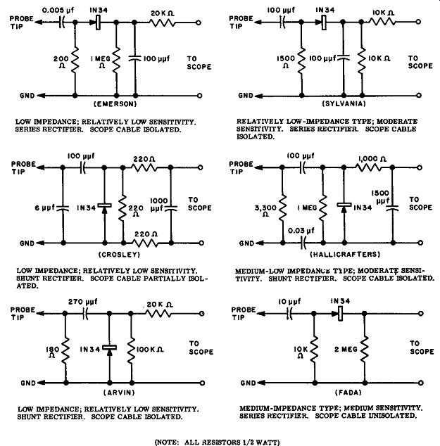
Fig. 7-12. Shop-constructed low- and medium-impedance demodulator probes suggested
by various tv receiver manufacturers for stage-by-stage i-f amplifier work.
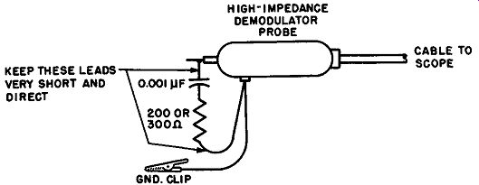
Fig. 7-13. A low-impedance demodulator probe is often required for proper
i-f stage-by-stage alignment or signal tracing. In the absence of this type
of probe, the technician may make use of a conventional high-impedance general-purpose
demodulator probe, in combination with a 200-ohm damping or swamping resistor
and blocking capacitor connected across it, to shunt down and flatten the response
of the tuned plate-circuit load to which the scope is applied.
7-11. The Low-Impedance Demodulator Probe for TV Front-End Work
A detuning problem similar to that described in Sec. 7-10 for i-f amplifiers exists when a conventional general-purpose demodulator probe is applied across the tuned plate circuit of an r-f amplifier tube during the course of tv front-end work. A special design of low-impedance probe suited for operation at the high tv station carrier frequencies is desirable in this work.
The circuit arrangement for a special shop-constructed low-impedance de modulator probe which has proved quite satisfactory for front-end work is shown in Fig. 7-14B. It can be seen that this is a low-impedance device which flattens the resonant response of any r-f circuit across which it may be applied. To cut lead length to an irreducible minimum, it is suggested that the probe be constructed without a housing or tip as would be done in the case of i-f probes.
Instead, the components should be joined with the shortest possible leads, as illustrated in Fig. 7-14A, and the probe tip should consist of a very short length of pigtail lead protruding from the button capacitor. If desired, a small hook may be bent in the lead for convenient connection. There is no ground lead, instead, there is a very short length of pigtail left protruding from the lN34A crystal diode which may be soldered to a clamp fitted around a small Alnico magnet. The magnet will serve to make connection to the receiver chassis near the base of the tube without adding the mechanical bulk and stray reactance of an alligator clip. The output lead labeled S connects to the input cable of the scope.
In use, the small hook at the button capacitor terminal is hooked over the r-f plate lead at the tube-socket plate terminal, and the magnet is placed on the chassis near the tube base. The r-F tube provides isolation between the low input impedance of the probe and the grid circuit of the tube; thus the circuit response up to and including the grid circuit of the tube is truly displayed. At the same time, the low input impedance of the probe flattens out the resonant response of the plate load of the tube, which would be partially detune by any other type of probe, leading to substantial distortion in the display.
Another special front-end probe arrangement, and details concerning its use, are discussed in Sec. 7-28.
7-12. Use of a Cathode-Follower with a Demodulator Probe
Although cathode-follower probes are not in general use in service work, the use of a cathode-follower is often suggested as another means of reducing the loading and detuning effects of demodulator probes. The use of a cathode follower ahead of a demodulator probe is especially helpful if it is desired to do quantitative work on high-impedance tuned circuits, since the demodulator probe loads the tuned circuits rather heavily and as a result the true voltage of the test signal is not indicated. The cathode-follower provides a very high input impedance even at 4 or 5 mhz, and does not disturb circuit operation. For this reason, it should be noted that two arrangements of the demodulator probe and the cathode-follower are possible:
(1) Cathode-follower feeding directly into demodulator probe, and from demodulator probe into shielded cable and scope.
(2) Cathode-follower feeding directly into shielded cable, and from shielded cable to demodulator probe located at the vertical-input terminals of scope.
Chief characteristics of these arrangements are: (1) Extends effective frequency-response range of scope vertical amplifier by demodulating the signal. Cathode-follower provides high input impedance to test circuit. Demodulator probe tends to distort the reproduced waveform at some modulating frequencies due to the effect of capacitance of probe cable on the time constant of the demodulator.
(2) Accomplishes the same purpose as (1 ), but eliminates the effect of cable capacitance on the demodulator probe. Therefore, reproduced waveform is much less distorted.
The cathode-follower described in Sec. 5-11 and illustrated in Fig. 5-22 is suitable for this purpose. The tube can be powered from the heater- and plate supply circuits of the scope.
When the response characteristic of the vertical amplifier of the scope being used is sufficiently wide so that the amplifier can satisfactorily respond directly to the carrier frequencies comprising the modulated signal being checked, the de modulator probe is not required. The cathode-follower working into a shielded cable may then be applied directly to the vertical-input terminals of the scope...
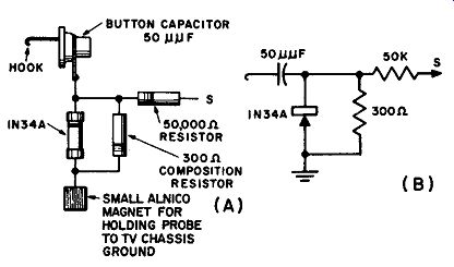
Fig. 7-14. (A) Parts and wiring arrangement, (B) schema tic circuit diagram
of a special low - impedance demodulator probe utilizing a button-type capacitor
and very short leads, for effective application in circuits operating at frequencies
above 100 mhz. The button capacitor receives the terminal stud of the crystal
diode directly, thus minimizing lead length. The button capacitor is of the
type which is provided with a stud which serves conveniently as a probe tip.
This probe will be found very useful in making operational checks of tv front-end
circuits, and also permits practical stage-by-stage investigation and alignment
to be performed.
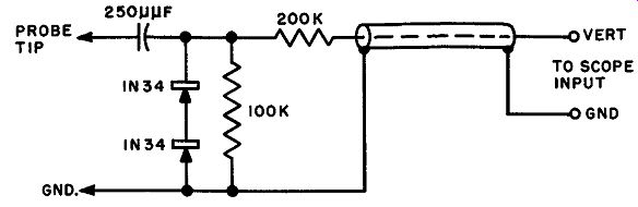
Fig. 7-15. By employing two crystal diodes in series, the voltage-handling
capability of the demodulator probe is doubled.
...and the arrangement, which has very high input impedance even at 4 or 5 mhz, may be used to good advantage to minimize loading of the circuits under test when signal-tracing the video-amplifier or sync circuits.
7-13. Demodulator Probe with Large Voltage-Handling
Capability
When a crystal probe is to be used in a relatively high-level signal circuit, such as at the output of a video amplifier having a substantial margin of output, it is sometimes found that the signal voltage applied to the probe is sufficient to weaken or burn out the crystal diode. In such applications, it is possible to connect two crystal diodes in series, to double the voltage-handling capability of the probe, as shown in Fig. 7-15.
7-14. Balanced-Input Crystal Demodulator Probes
An easily constructed balanced-input crystal demodulator probe, of the type shown in Fig. 7-16A, is very useful for checking the modulated voltage existing at any point along a balanced transmission line, or at a balanced output circuit such as that of a balun, the output of a tv converter or booster, etc. The probe offers a balanced input to such a circuit, while the output is an unbalanced one to match the scope input circuit. The series-rectifier arrangement employed, provides minimum input capacitance to the probe, and hence the least disturbance of line impedance. Because d-c voltage is seldom present in such lines, a series arrangement is practical; also no blocking capacitor is required. The 250-µµf charging capacitor is charged alternately by the diodes, and the series resistor serves to isolate the shielded cable from the high-frequency portion of the circuit.
Observe that the two diodes in the probe do not conduct simultaneously.
Insofar as the instantaneous voltages in the 2-wire line are concerned, when the input signal to one diode is positive, the input signal to the other is negative.
These polarities alternate at the carrier frequency, thus the diodes conduct alternately. The output of the probe, is the modulation envelope of the line voltage, and may be displayed on a scope (or a d-c vtvm may be employed for purposes of voltage indication).
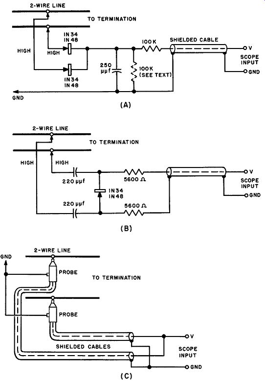
Fig. 7-16. (A) Shop-constructed balanced-input probe arrangement for checking
the voltage existing at any point along a 2-wire line. Such probes are useful
for impedance-match (standing-wave) testing procedures. (B) Sensitive arrangement
employing only one diode and requiring no ground return. (C) Method of using
two conventional general-purpose demodulator probes for the purpose, instead
of a special balanced-input probe.
The r-f ground lead to the line termination carries r-f voltage and should be kept as short as the "high" leads.
Although it appears, with the balanced-input shown here, that no d-c return path exists when a scope with an input blocking capacitor is used, such is not the case. The d-c return path is provided through the finite back resistance of the crystal diodes and the voltage-source resistance. If diodes with unusually high
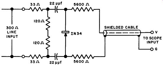
Fig. 7-17. When operating at uhf, the balanced-input demodulator probe net
work can be tapped down on the load, as shown here, so that the capacitance
of the network does not seriously disturb the line termination. Courtesy: RCA
back resistance are used, it may be necessary to shunt the 250-µuf capacitor
with the 100,000-ohm bleeder resistor indicated.
A simplified, though somewhat less sensitive arrangement employing only one diode, is shown in Fig. 7-16B. It also has the advantage that a ground return is not required to a center tap on the line termination.
A pair of conventional general-purpose demodulator probes may also be employed, instead of a special balanced probe, in the manner shown in Fig. 7-16C. It is sometimes stated that the elaboration represented by the balanced-input type probe is unjustified, and that a single-ended probe contacted to one side of the line would serve the purpose just as well. However, a single-ended probe will give the same information as the balanced-input probe only if the line is actually balanced to ground. In many cases, twin-lead lines are not balanced to ground, and different voltages may be found between each conductor and ground. Accordingly, if a single-ended probe is used in such cases, it might be falsely concluded that the standing-wave ratio is low, whereas a test with a balanced-input probe will show the actual standing-wave ratio which is present.
What is more, the use of an unbalanced probe will usually alter the actual balance of the line itself.
Practical applications and test setups for the use of the balanced-input de modulator probe are discussed in Sec. 7-27.
When the frequency of test is high, and the input capacitance of the balanced-input demodulator probe arrangement disturbs the termination of the line, it is good practice to tap the probe network down on the load, as shown in Fig. 7-17. This arrangement is satisfactory for tests at uhf. A probe of this type is useful for demodulating the output sweep voltage from a uhF converter during alignment of the converter. This probe is arranged to offer a balanced input of 300 ohms.
7-15. Voltage-Doubler Crystal Demodulator Probe
Increased probe sensitivity over that obtainable with conventional series type or shunt-type demodulator probes is often required in some applications.
This can be obtained by utilizing the voltage-doubler principle explained in Sec. 6-9 and Sec. 6-17. This circuit adds the positive-peak value of the modulating waveform to the negative-peak value, and thereby delivers an output proportional to the peak-to-peak value of the modulating waveform. If the modulating voltage has a symmetrical waveform (such as a sine wave or a square wave), double the amount of deflection will then be obtained on the scope screen. When the modulating-voltage waveform is asymmetrical, a value less than this will be obtained, depending upon the degree of dissymmetry present.
The schematic circuit diagram of a useful voltage-doubler type demodulator probe which has considerable utility in some of the tv troubleshooting procedures described later in this section is shown in Fig. 7-15A. A representative commercial probe is illustrated in Fig. 7-15B. Although the voltage-doubler feature makes the sensitivity of this type of probe quite high, its input impedance is relatively low, and the waveform distortion may be appreciable. It is possible to construct a practical probe of this type with a frequency response flat to approximately 150 me; such a probe will be useful for comparative indication at still higher frequencies. This probe will also offer a high degree of 60-cyde hum-voltage rejection.
Fig. 7-18. (A) Voltage-doubler type of demodulator probe for obtaining increased output and greater deflection on the scope than is provided by conventional type of demodulator probes. (B) A typical commercial probe of this type. This probe is provided with its own shielded cable for connection to the scope input terminals. (B) Courtesy: Scala Radio Co.
(A) (B)
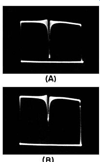
Fig. 7-19. Effect of front-to back resistance ratio of the crystal
diode in a demodulator probe upon the modulation waveform fidelity of the
probe.
(A) Modulation - waveform output obtained when a crystal diode having a low front to-back ratio was employed.
(B) When a crystal diode having a high front-to-back ratio is employed. The high front-to-back ratio provides more output voltage, but the longer time constant which results from the higher back resistance makes the probe filter circuit unable to follow rapid changes in the shape of the modulation envelope. Consequently, only part of the long sharp dip at the center of the modulation waveform appears in (B).
The maximum allowable safe input voltage for a voltage-doubler probe is approximately the same as for a conventional type probe using the same type of crystal diode. For a 1N34 diode, this is approximately 20 volts rms and 28 volts peak. If a d-c component is present, this component should not exceed approximately 600 volts (which is the rating of the series capacitor specified here). In general, when a conventional type of demodulator probe does not provide ample deflection on the scope screen, the voltage-doubler type may be utilized for greater output, even though its comparatively low impedance has a tendency to load down the circuits to which it is applied. The technician should keep in mind however, that a conventional type of probe will provide flat frequency response up to much higher carrier frequencies. Some technicians use a voltage-doubler type as their most useful general-purpose demodulator probe.
Since a voltage-doubler demodulator probe utilizes shunt rectifiers in combination with relatively low values of series charging capacitance, a 60-cycle hum voltage is greatly attenuated with respect to r-f or i-f voltage. For this reason, special tests in heater circuits, age lines, and d-c supply lines are greatly facilitated. The technician can usually check for "hot" bypass or decoupling capacitors, heater "hash", or video voltage in age lines without encountering serious disturbance of the scope screen pattern from hum voltage or heater voltage (see Sec. 7-32). The technician who has both a conventional-type demodulator probe and a voltage-doubler demodulator probe available, is sometimes puzzled by the apparent ability of the voltage-doubler probe to provide more than double the output of the conventional probe in some tests. In other tests, the voltage doubler probe provides less than double the output of the conventional type of probe. Such apparent discrepancies in the operation of the two probes is due to the fact that the carrier wave of the signal under test is not a symmetrical wave, and accordingly the wave has a greater positive excursion than negative excursion (or vice versa). To make a meaningful check of a voltage-doubler probe against a half-wave probe, the operator should utilize a signal generator which provides a signal having good symmetrical waveform (small harmonic content).
7-16. Design and Construction Hints for Shop-Constructed Demodulator Probes
Satisfactory performance of a demodulator probe is dependent upon proper mechanical construction, as well as the use of a suitable circuit arrangement and circuit constants. The construction is simple in most cases, provided that the required consideration is given to high-frequency factors such as the proper lay out of components to insure short leads, use of composition resistors and suitable capacitors for the high-frequency circuits, and minimizing of stray capacitance in mounting the components in the probe case. The exploded-view illustration in Fig. 7-9C, and illustration B in Fig. 7-18, reveal a considerable amount of information concerning how these requirements are met in successful commercial demodulator probes.
The crystal diode (s) used must have a relatively high front-to-back resistance ratio, and also be able to accommodate reasonably high a-c signal voltage without loss of sensitivity or burnout. The 1N34 or 1N34A, and the 1N48 type crystal diodes are widely used in these probes because of their satisfactory characteristics. The crystal diode should be selected, as the front-to-back ratios of commercial diodes vary considerably, affecting both the sensitivity and the input impedance of the probe.
The effect of low front-to-back ratio of a crystal diode used in a demodulator probe is illustrated in Fig. 7-19. Even when comparatively strong signal-generator signals are employed in the tests, excessive hash resulting from pickup of strong stray 60-cycle and 15.75- khz fields about a tv chassis may obscure the scope trace unless the probe is properly shielded and a shielded output cable is used. Be cause the probe must be used in cramped spaces, it must be well insulated to avoid shorts during use.
Fig. 7-20. Method of testing a probe to determine if its shielding is adequate
to prevent spurious-voltage induction into its components or wiring by the
extraneous fields around a tv chassis. Use the very smallest amount of exposed
resistor leads in this arrangement.
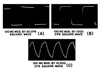
Fig. 7-21. Demodulating ability of a conventional type de modulator probe
for modulation of various frequencies. It can be seen that the demodulating
ability of the probe decreases as the modulation frequency increases, and distortion
of the modulation waveform results. A voltage doubler type of probe is usually
more unfavorable than the conventional type in this respect.
A simple method for checking a shop-constructed or a commercial probe to determine whether or not its internal shielding is adequate to prevent spurious voltage induction into its components or wiring by extraneous fields around a tv receiver is illustrated in Fig. 7-20. The terminals of the probe are shunted by a 5,000-ohm resistor (to simulate typical circuit impedance), and the probe 10 using is then moved about the receiver chassis. In particular, the vtvm or scope to which the probe is connected, should be watched while the probe is brought near the output transformers, picture tube, oscillator transformers, yoke, and power transformer. If the probe is adequately shielded, no deflection will be obtained on the instrument.
7-17. Demodulating Ability of Crystal Demodulator Probes Somewhat Limited
The output network of a demodulator probe is a low-pass filter as has been explained. Its contents must be selected to provide adequate r-f filtering action, but if the filtering is excessive (time constant too long), a 60-cycle square-wave modulation envelope, for example, will be distorted by the probe.
Both conventional and voltage-doubling demodulator probes distort the modulation waveform increasingly as the modulation frequency increases. Refer ring to Fig. 7-21A, it is apparent that the output filter of a conventional demodulator probe may be designed to pass a 50-cycle square-wave modulation envelope practically without distortion. This means that the probe is entirely satisfactory for use in video-amplifier adjustment, single-stage response checks, and similar applications where the sweep of the test signal is made to occur at a rate in the vicinity of 50 to 60 hz, thus creating an output wave envelope of the same frequency, and of the same general class as a square wave.
However, if the square-wave modulation frequency is raised to 1,000 hz, high-frequency attenuation and phase shift begin to make their appearance and the diagonal corners of the reproduced square wave exhibit rounding, as shown in Fig. 7-21B. When the square-wave modulation frequency is increased to 10,000 hz as in :Fig. 7-21C, it is seen that severe high-frequency attenuation and phase shift occur. (A voltage-doubler type probe is usually more unfavorable than the conventional type of probe in this respect.) Accordingly, the technician would not expect the demodulator probe to reproduce a horizontal sync pulse, for example, without severe distortion.
The ability of the probe to deliver higher-frequency modulation waveforms with improved fidelity may be increased by eliminating the series isolating (filter) resistor so that the probe circuit works directly into the scope input cable.
Unfortunately, when this is done, the probe does not usually respond satisfactorily to the higher i-f and r-f carrier frequencies because the shielded probe cable is then enabled to exhibit resonance effects at various frequencies, as is explained in part 2 of Sec. 7-4. Consequently, the improvement in probe ability to reproduce the modulation waveform with better fidelity is then partially offset by the reduction in carrier-frequency range over which the probe will operate without disturbing cable-resonance effects. The effect on the fidelity of the modulation waveform, of employing various values of isolating resistance in a typical demodulator probe is illustrated in Fig. 7-4.
7-18. Check of Probe Time-Constant Suitability for an Intended Test-Signal Sweep Width
When the sweep width of a sweep generator used in a test is increased, any variations present in the slope of a response curve being displayed on a scope by means of the sweep input signal become steeper. Therefore the R-C filter in the output circuit of the demodulator probe being used is called upon to charge and discharge more rapidly, if the output voltage is to rise or fall in accord with very rapid changes in the modulation waveform.
For a practical illustration of this situation refer to Fig. 7-22, which shows a video response curve obtained by applying the output from a video sweep generator to the input of a video amplifier, and connecting a demodulator probe and scope to the output of the video amplifier. Because the sweep width used here is considerable, the rate of change of the response curve is also considerable in the middle portion, where the output of the generator goes through zero frequency. Because of this rapid change, the R-C filter network in the output circuit of the demodulator probe is unable to respond quite as fast as necessary, and the result is that the two curves do not appear at the same height. At lesser sweep widths, this difference disappears.
Fig. 7-22. Example of video response curve distortion resulting from too long
a time constant in the demodulator probe for the video sweep width employed.
The video sweep generator is operating at considerable sweep width; the output
from the demodulator probe does not drop to zero voltage at the zero-frequency
point (center), and the two responses differ in height, be cause of the excessive
charge and discharge time of the probe filter for the high rate of modulation
change which occurs at this point.
Fig. 7-23. Traces of demodulated output from a video sweep generator in a test to determine whether the time constant of the demodulator probe filter is suitable for the sweep width that will be employed in the test. (A) Probe time constant is suitable for the application, since the zero frequency point falls to zero voltage. (B) Probe time constant too long for the application, since the zero-frequency point does not fall to zero voltage. The extent to which the zero frequency point remains above zero voltage is an indication of the excess in the time constant of the demodulator probe. (A) and (B) taken when a zero-volt reference line is used. (C) When zero-volt reference line is not used ( retrace unblanked), the trace and retrace are exact replicas, if the probe time constant is satisfactory, showing that any difference in the shape of the curve when going toward and away from zero frequency is caused by the sweep generator, and not by the demodulator probe.
(D) The trace and retrace are not exact replicas here, and the extent to which the shape of one differs from that of the other is an indication of how excessive is the time constant in the demodulator probe.
This is a useful test to determine whether the constants of the demodulator probe filter are suitable for the job at hand. The method of interpreting such a test is illustrated in Fig. 7-23.
7-19. Effect of Crystal-Diode Nonlinearity upon Demodulator Probe low-Voltage Response
A crystal demodulator probe is nonlinear for input signals of low voltage level (the same as a rectifying type of probe), due to the curvature of the crystal diode characteristic at low voltage inputs. The curvature of the characteristic from 0 to approximately 0.75 or 1 volt is quite appreciable (see Fig. 6-12). As a practical example of the effect of this nonlinearity of a crystal demodulator probe at low signal levels, when a 50 percent modulated signal of 0.6 volt peak to-peak being applied to a crystal demodulator probe was reduced to one-tenth of its value, or 0.06 volt peak-to-peak, the output from the probe might have been expected to drop to one-tenth of its first value. However, because of the nonlinearity of the crystal diode, the output from the probe actually dropped to one-twenty fifth of its first value.
One result of this inherent nonlinearity is to make the apparent observed output variation from a video sweep generator greater than it is in fact, and greater than it would appear were the output from the generator applied through a linear amplifier. Accordingly, when the technician is checking the output from a sweep generator with a demodulator probe and scope, substantial observed variations from flatness must first be considered with respect to the possibility of being exaggerated due to the nonlinearity of the crystal diode characteristic, before the generator is blamed for the departure from flatness.
This nonlinearity will also cause some waveform distortion at the high attenuation portions of frequency response curves, if the voltage input to the demodulator probe during the taking of such curves falls to a value low enough to cause the crystal diode to operate nonlinearly.
7-20. Effect of Accidental Application of D-C Bias to Crystal Diode in Probe
A small d-c bias voltage applied accidentally to the crystal diode of a de modulator probe (or a rectifying probe) while ii:. is being used in a test can render it useless for most tv test work. A d-c bias can result when the grid bias on the first vertical-amplifier tube in the scope backs up into the probe through a leaky scope input blocking capacitor. This bias may effectively disable the crystal diode. A leaky probe input series capacitor may also be responsible for allowing a bias voltage to be applied to the crystal diode from the circuit under investigation.
If the crystal in a "defective" probe is replaced and the probe still does not work with the new crystal, check for the presence of d-c voltage across the output terminals of the probe, using a vtvm for this check. If the presence of such voltage is indicated, check for leakage in the blocking capacitor in the probe and scope input circuits.
7-21. Position of Demodulated Waveform on Scope Screen
It should be observed that when a demodulator probe is used with a d-c scope, the same facility is obtained as if a zero-volt reference line were available from the sweep generator employed with it. This principle is illustrated in Fig. 7-24, where a single-stage i-f response characteristic is shown displayed on an a-c scope in part A, and on a cl-c scope in part B. The zero-volt level is unknown when the a-c scope is used, and the operator will have difficulty in checking the gain of this stage. However, when a d-c scope is used, the curve rises up above ...
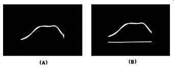
Fig. 7-24. Stage checks with a demodulator probe are facilitated by the use
of a d-c scope, since the resting level indicates the zero-volt reference,
and the peak, or peak to-peak, voltage is indicated on the screen. (A) A single
stage response as seen on an a-c scope. ( B) The same response characteristic
as seen on a d-c scope. This photo is a double exposure in order to show the
zero-volt reference line.
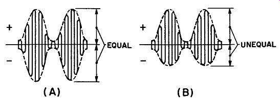
Fig. 7-25. (A) Symmetrical modulated r-f output signal waveform usually approached
only by costly laboratory-type signal generators. (B) Service technicians find
that the modulation envelopes of the modulated signals supplied by typical
service-type signal generators are often unsymmetrical, as shown here. This
influences the proper crystal-diode polarity which must be used for greatest
sensitivity in a single-diode type demodulator probe when operating with such
signals. The probe will appear to be insensitive if polarized to accept the
negative-peak excursion, and to reject the positive-peak excursion, of the
type of signal shown in (B).
... the resting level of the trace and indicates the peak voltage values of the output when a conventional type demodulator probe is employed, and the peak-to-peak value when a voltage-doubler type demodulator probe is used. The resting level of the trace is the zero-volt level, when a d-c scope is used. Of course, the same information can be obtained on an a-c scope, if the sweep generator provides a zero-volt blanking function.
7-22. Effect of the Polarization of the Crystal Diode in Demodulator Probes
The crystal diodes in Figs. 7-3, 7-6, 7-7, 7-9, etc. are shown connected into the probe circuit with the proper polarity to make the center conductor of the probe cable positive. This will produce a right-side-up trace of the modulating waveform on any scope which is correctly polarized for upward deflection from a positive voltage. Reversing the crystal polarity in a series or a shunt type of single-diode demodulator probe causes the waveform to invert on the scope screen.
Of greater importance, is the fact that the crystal polarity must be correct if maximum sensitivity is to be realized when viewing modulated waveforms having unequal positive and negative amplitudes. The modulated output signals of some signal generators employed by service technicians are frequently of this type, and when a demodulator probe is used with a scope to view them, the polarization of the crystal diode in the probe is a matter of importance.
Consider the illustrations shown in Fig. 7-25. In part A we see a highly modulated r-f wave which has a symmetrical waveform. If all signal generators delivered a symmetrical waveform of tl1is sort, the polarization of the crystal in the demodulator probe would not be a matter of concern, since both the positive and the negative peaks of the modulated signal have the same amplitudes.
However, the technician will frequently be under the necessity of utilizing test signals having modulated waveforms of the character shown in Fig. 7-25B. Since the positive peak voltage of this modulated wave is considerably greater than its negative peak voltage, the probe output would be less and the crystal probe would be judged to be insensitive if the crystal diode were to be connected in the circuit with a polarity so as to accept the negative-peak excursion and to reject the positive-peak excursion. For general work, some technicians keep on hand a positive-peak general-purpose probe and a negative-peak probe.
These considerations also affect the sensitivity of signal-tracing operations when the modulation envelope of the signal generator output is asymmetrical, as well as when generators are being calibrated against crystal oscillators. In a typical instance, three times as much deflection was obtained on the scope merely by reversing the polarity of the crystal diode in the demodulator probe.
Other cases have been observed in which the difference was considerably greater.
Service technicians frequently find, therefore, that the apparent sensitivity of conventional types of crystal demodulator probes is greatly affected by the polarity with which the crystal diode is connected into the probe circuit. The foregoing considerations apply only to probes utilizing a single crystal diode.
They do not apply to voltage-doubler probes which effectively add up the positive peak and the negative peak value of the waveform. With them, the output is proportional at all times to the peak-to-peak value of the waveform.
7-23. Demodulator Probe Exhibits Feed-through at Low Carrier Frequencies
A conventional crystal demodulator probe exhibits a certain amount of feed-through at low frequencies. This feed-through to the output consists of un-rectified and unfiltered voltage having the same waveform as the applied voltage.
To consider a simple example, it might be supposed that if the output from an audio oscillator were applied to a crystal demodulator probe, that the scope would display half cycles of rectified voltage on the screen. Actually, such a test will quickly convince the reader that there is a substantial amount of sine-wave feed-through voltage at these comparatively low frequencies.
The maximum feed-through for one conventional crystal demodulator probe tested was found to occur around approximately 10,000 cycles. At 500 cycles, the feed-through fell to a very small value, because of the reactance of the particular value of series input capacitor used in this probe. At 200,000 cycles, the feed through again fell to a very low value because the R-C filter in the output of the probe did not permit appreciable passage of frequencies in the vicinity of 0.2 mhz.
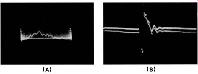
Fig. 7-26. An attempt to obtain signal pickup for a de modulator probe by
means of a floating tube shield may be disappointing unless the horizontal-
and vertical-sweep circuits of the tv receiver are first disabled. (A) Interference
from stray field of horizontal sweep circuit. ( B) Interference from stray
field of vertical sweep circuit.
7-24. Stray-Field Interference Intensified when a Demodulator Probe is Used in High-Impedance Circuits
Upon occasion, the technician finds it more convenient to do a signal-tracing job top-chassis, by placing a floating tube shield over successive tubes, and using a demodulator probe to demodulate the modulated high-frequency voltage induced in the tube shield, for display on the scope. This method depends for operation upon the fact that a floating tube shield is capacitively coupled to the plate of the tube over which the tube shield is placed. This is a high-impedance arrangement, and is susceptible to pick-up of stray fields from the vertical and horizontal sweep-circuits of the receiver, which interfere with the test. Typical interference situations are shown in Fig. 7-26. The method works satisfactorily only if the sweep circuits are disabled to prevent the interference.
The floating tube-shield method is usually more satisfactory than the use of test-point adapters in making high-frequency circuit tests (such as those at the front end of the tv receiver) from top-chassis, because the additional lead inductance introduced by the test-point adapters often seriously detunes the circuits under test. Top-chassis tests are very convenient for preliminary troubleshooting procedures in the customer's home.
7-25. Use of a Demodulator Probe for Checking TV High-Frequency Current Waveform
The technician should remember that a scope is a microammeter as well as an electronic voltmeter. However, it is not always recognized that the scope may be used as a high-frequency microammeter in tv testing, as well, when it is applied in a suitable manner with a crystal demodulator probe. In order to develop the current waveform in a high-frequency circuit, the current must be passed through a non-inductive resistor.
Many video i-f amplifiers utilize cathode degeneration in order to stabilize the circuit operation. In a typical receiver, the cathode resistors have a value of 82 ohms. The video signal current passes through these resistors and develops a voltage drop across them. This voltage drop may be applied to a demodulator probe to display the waveform of the video current in the cathode circuit, as shown in Fig. 7-27. (If these resistors are not already present in the circuit, they can be introduced for the test.) This method of test can also be employed in the cathode circuits of the 4.5-mhz sound i-f circuits where probe loading, when the probe is connected in the more conventional manner in the plate circuit (see Sec. 7-10), is a more severe problem than in the picture i-f amplifier, due to the narrow bandwidth and higher Q of the 4.5-mhz circuits.
From the practical point of view, it is often necessary to use a scope pre amplifier to obtain satisfactory deflection when high-frequency currents are displayed by this method. However, the use of a voltage-doubler demodulator probe, with its relatively high output, is of some help in this respect. A high quality audio amplifier having low hum level makes a very satisfactory scope preamplifier.
7-26. Demodulator Probe Application in TV Receiver Servicing
Crystal demodulator probes can be used in a number of practical and important circuit-alignment and test procedures in tv service work. Figure 7-28 shows the receiver sections in which they are usually applied. They can be used in signal tracing in the r-f, i-f and video amplifiers; in buzz-pulse analysis in 4.5-mhz amplifiers, or in the sound i-f amplifier strips (split-sound tv); in ratio detector curve marking; in marker-generator calibration; in stage-by-stage alignment, and in any other test which requires demodulation of the signal, so long as the peak test voltage does not exceed approximately 28 volts.
Signal tracing is a straightforward procedure, and can be done in the same general manner as conventional signal tracing of a broadcast receiver. The de modulator probe picks up the modulated high-frequency signal at any point in the tuned circuits or in the video amplifier, and will display the waveform upon the scope screen.
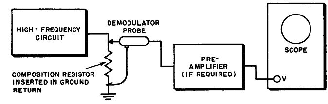
Fig. 7-27. The waveform of modulated high-frequency currents in a tv receiver
can be displayed on a scope screen with the aid of a demodulator probe and
a small resistor. A pre-amplifier will often be necessary to obtain sufficient
deflection on the scope screen when a small resistor is used. A large value
of resistance is likely to disturb the circuit action, and will also result
in a distorted waveform due to the effect of the input capacitance of the demodulator
probe.
It should be noted that if signal tracing is necessary in tv r-f circuits, it will often be necessary to use a swept signal, rather than a tv station signal, because the signal voltage may otherwise be too low for satisfactory deflection on the scope screen-especially in the early stages of the receiver.
By the use of the signal-tracing techniques, it is possible to pinpoint a dead or weak stage, a regenerative stage, or an oscillating stage, in the r-f, i-f, video, and sound amplifiers. A dead stage develops no deflection on the scope screen.
A weak stage will exhibit less deflection than the previous stage, i.e., a loss instead of a gain. A regenerative stage will show up in either of two ways, depending upon whether a sweep signal or a tv station signal is being used in the circuits.
A sweep signal which passes through a regenerative stage will show an extremely large response at one end or in the middle, but very low response over the rest of the curve. If the regeneration is excessive, spurious markers may also appear.
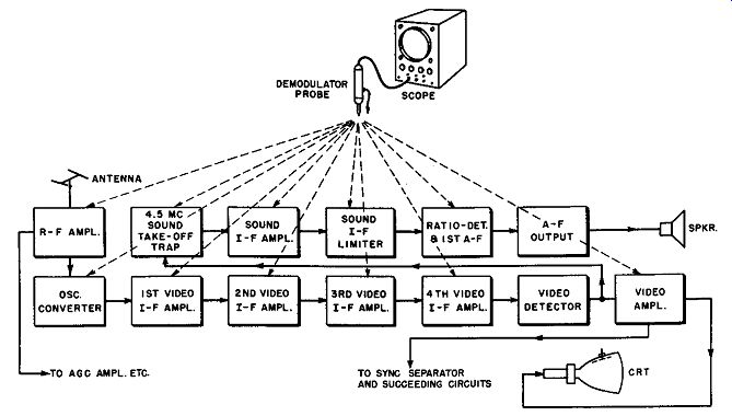
Fig. 7-28. Sections of a tv receiver in which demodulator probes are widely
used in visual circuit-alignment and troubleshooting procedures.
An oscillating stage shows up as a response curve which has gone to pieces and also often exhibits undershoot due to the grid overdrive and flow of grid current.
Strong oscillation may paralyze the stage, which may then be confused with a dead stage. However, the supplementary use of a vtvm and a high-frequency rectifying probe will distinguish between the two cases, since the oscillating stage will cause a large deflection on the vtvm (when connected to the grid), whereas a dead stage causes no deflection of the pointer.
If a station signal is used for the tracing procedure, regeneration may show up as severe distortion of the composite video signal, either with the equalizing pulses much lower than the level of the vertical sync probe, or with severe over shoot and ringing along the top of the vertical sync pulse.
Some of the more important operating requirements of demodulator probes for use in various tv servicing applications have been outlined in Sec. 7-8, and the reader is advised to review them at this point. Additional requirements will be pointed out in the discussions which follow. Both series- and shunt-type de modulator probes are employed in this work; the series type being the more sensitive for general signal-tracing purposes, but also providing less attenuation to objectionable 60-cycle and 120-cycle hum voltage with respect to r-f or i-f voltage. This latter characteristic, plus the output-waveform distortion it produces, makes the series-type probe the least suitable one for video-amplifier testing. Consequently, shunt-type demodulator probes are more widely used in this particular work. The voltage-doubler type demodulator probe provides increased sensitivity that is advantageous in many tests, but its useful carrier-frequency response range is lower than that of the other types.
It should be remembered that any probe which employs crystal diodes can be damaged by excessive input voltages. Ordinarily, such probes will not be dam aged by application of the signal voltages from the r-f, i-f, or 4.5-mhz circuits.
Any contact with the high-voltage sweep circuits, accidental or otherwise, will immediately burn out the crystal diode (s). Practical general-purpose demodulator probes designed for tv receiver work usually have moderate sensitivity, an input capacitance approximately equal to that of a picture tube, are non-resonant out to at least 225 mhz, and have a time constant suitable for demodulating carrier frequencies which have been modulated by frequencies as low as 60 hz.
The service technician should never forget that a crystal demodulator probe not only introduces an insertion loss in the circuit, but also causes a certain degree of output-waveform distortion. Therefore, whenever the carrier frequencies comprising the modulated signal under observation are within the flat frequency-response range of the vertical amplifier of the scope which is to be used, the demodulator probe should not be employed. The test signal should be applied direct to the scope input terminals instead, and the carrier of the signal displayed directly. (A capacitance-divider type high-voltage probe, or a low capacitance probe, may be required ahead of the scope in some circuits, such as the high-voltage horizontal-output circuit and the horizontal-oscillator circuits, respectively, see Sections 2 and 6.)
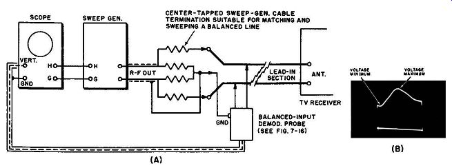
Fig. 7-29. (A) Checking for mismatch between the characteristic impedance
of the antenna lead-in and the input impedance of the tv receiver, by means
of a balanced-input type demodulator probe and scope. Note that the lead from
the center-tapped sweep-generator cable termination to the Gnd terminal of
the probe carries the r-f sweep voltage. It therefore should be kept as short
as the "high" leads to the probe, in order to avoid distortion in
the response trace. (B) Mismatch between the lead-in impedance and the input
impedance of the front end of a tv receiver is indicated here by the bump in
the response trace. If perfect impedance match exists over the swept-frequency
range, a flat response trace will result.
A number of helpful demodulator probe selection and application hints pertaining to several of the more important uses of such probes in tv service work, are presented in the following sections of this Section.
7-27. Use of Balanced-Input Type Probe for Checking Impedance Match of Transmission Line to Antenna or Receiver
A balanced-input demodulator probe arrangement, such as is described in Sec. 7-14, is very convenient for use with a scope to quickly check the frequency response of a transmission line; or the degree of mismatch existing between the characteristic impedance of an antenna lead-in and the impedance of the antenna, or between it and the input impedance of the front end of the tv receiver, converter, or booster with which it is associated. The balanced output circuits of signal generators, the characteristics of interference-elimination stubs, the impedance match between a balun and its load, or that between a converter or booster output circuit and the tv receiver front end input circuit, may also be checked in the same manner. The equipment setup for checking impedance mismatch between an antenna lead-in and the input circuit of the tv receiver's front end is illustrated in Fig. 7-29A. Similar setups may be used for other tests of this type.
A sweep voltage of suitable center frequency and deviation is fed to the input end of the lead-in, balun, or other device, by a properly terminated sweep generator, and the balanced-input demodulator probe is arranged to pick off the signal voltage appearing at either the input end as shown or at the other end (which is connected to the load to which it is supposed to be matched). If line mismatch is being checked, the transmission line should be at least 20 or 25 feet long so that appreciable standing waves can be developed at representative tv signal frequencies. The line should be kept away from metallic objects and have no sharp bends. If a perfect impedance match exists at all of the frequencies swept through (and a sweep generator which has a flat output characteristic is used), no variations in voltage will occur at the input to the balanced demodulator probe at any of the frequencies swept through, and a flat trace will there fore appear on the scope screen. If an impedance mismatch exists and standing waves are set up, the input voltage rises and falls in accord with the rise and fall of impedance seen at the source end of the line. This produces a response curve having pronounced peaks and valleys.
The degree of mismatch often encountered in practice is shown in Fig. 7-29B; here the highest voltage point resulting from the standing-wave pattern is approximately twice the voltage at the lowest point. However, much more severe conditions of mismatch may often be encountered. Such mismatch can be partially corrected by sliding a piece of tinfoil along the line to a suitable point.
However, a better method is to adjust the coupling of the antenna coil properly with respect to the r-f grid coil in the tuning strip. In this way, discontinuities are not introduced into the lead-in which could affect operation on other channels.
7-28. Demodulator Probe Application in TV Front-End Work
The signal-substitution method may be employed for troubleshooting tv receiver front ends. To determine whether the antenna signal is proceeding through the r-f stage to the mixer grid, connect a scope directly to the tap ("looker" point) usually provided on the mixer grid-leak. (It may be necessary to insert an isolating resistor of about 50,000 ohms at the end of the scope cable to avoid loading of the mixer grid circuit and detuning of the grid coil.) The grid of the mixer is usually operated at zero bias, so that a nonlinear or heterodyning action can take place. In consequence, there is a demodulated component at the mixer grid, as well as sum-and-difference frequencies, the difference frequency being accepted by the first i-f tuned circuit. Thus, the grid circuit of the mixer operates as a diode detector, and the plate circuit operates as an amplifier.
Therefore, with the scope connected to the mixer grid-leak "looker" point, the r-f and mixer input response curve should appear on the scope screen when a sweep signal is applied to the antenna terminals of the receiver. If a fixed frequency signal of a frequency approximately equal to that of the local oscillator is applied to the antenna terminals instead, a demodulated Lissajous pattern will be produced on the scope screen that is useful for adjusting the local oscillator to correct frequency. If a strong tv station signal is applied to the antenna terminals instead, a demodulated video signal display will be produced on the scope screen. In each case, the demodulated output from the mixed grid circuit is being used for display instead of the modulated r-f carrier, or the sum and-difference frequencies, or their harmonics, which are normally present.
If it is not possible to obtain a response trace at the mixer grid, it is necessary to check the response of the antenna and r-f grid coils separately, and to check the mixer coupling transformer separately.
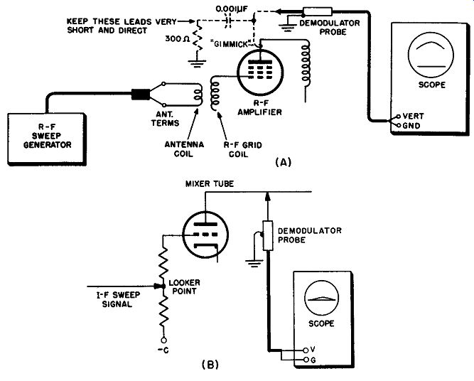
Fig. 7-30. (A) If the
test signal does not arrive at the mixer grid when trouble shooting the front
end, the response of the antenna coil and r-f grid coil can be separately
checked by the instrument setup shown here. A low-impedance de modulator probe
arrangement is required (see text). (B) A test setup which utilizes the "looker" point
on a front end as a signal-injection point to check the progress of an r-f
sweep signal through the mixer circuit. A demodulator probe and scope are used
to display the mixer output signal.
To check the antenna and r-f grid coils, the setup shown in Fig. 7-30A may be used. The special low-impedance high-frequency probe described in Sec. 7-11 is particularly well suited to this work. If a general-purpose type demodulator probe is employed instead, its input should be shunted with the 300-ohm swamping resistor and B+ blocking capacitor shown to load down the plate circuit of the r-f amplifier so that the response of the r-f input circuit appears only on the scope. Both resistor and capacitor leads must be very short and direct. If a special low-impedance probe of the type described in Sec. 7-11 is used, the swamping resistor and blocking capacitor are not required. Connection to the plate of the tube may be made by means of a "gimmick" consisting of a small loop of wire slid under the tube base and hooked over the plate pin. The demodulator probe is required here because the signal now being sampled for test is the modulated sweep output of the r-f tube.
In case it is inconvenient to use a "gimmick" for connection to the plate of the r-f amplifier tube, lift up the tube shield over the r-f tube far enough to clear the grounding ring, and apply the demodulator probe between the floating tube shield and chassis. The response curve will be distorted, but indication of the presence of test signal will be definite.
The "looker point" on a front end is also useful as a signal-injection point to check the mixer operation. Circuit (B) in Fig. 7-30 shows the test setup for this check, using a demodulator probe applied at the mixer tube plate. The output from the mixer is quite small, as the sweep signal is attenuated by the resistance associated with the looker point. However, comparative gain measurements can be made as for the r-f stage.
Somewhat more output is obtained in this test, and misleading spurious cross beats on certain channels will be prevented, if a dummy tube is used in the front end to disable the local oscillator. When the oscillator is operating, rectified voltage from the local oscillator appears across the crystal diode in the demodulator probe and biases the crystal to a less favorable operating point on its characteristic.
Alternately, the mixer stage can be checked in combination with the local oscillator, by injecting r-f sweep voltage at the looker point with the local oscillator operating, and permitting it to beat with the local-oscillator voltage. The difference beat is then accepted by the mixed plate circuit, and displayed on the scope screen.
Regeneration, or oscillation present in the r-f or mixer stages can be tracked down by the methods outlined in Sec. 7-26 for such troubles.
7-29. Demodulator Probe Application in Video I-F Amplifier Work
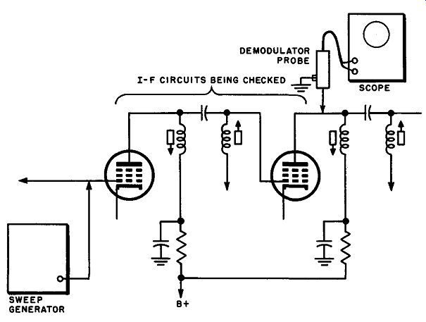
Fig. 7-31. Conventional method of checking the alignment, or testing the response,
of a single stage of a video i-f amplifier, using a demodulator probe and scope
for visual indication.
The demodulator probe finds some of its most important applications in visual stage-by-stage alignment and signal-tracing operations performed in the i-f amplifiers of tv receivers (see Fig. 7-28), because the carrier frequencies of the test signals (up to about 50 mhz) used in such work are usually well beyond the frequency range of the vertical amplifiers of service-type scopes.
The danger of the possible harmful circuit loading, stage detuning, and regeneration' or oscillation which may be caused by the indiscriminate use of a conventional general-purpose demodulator probe in i-f amplifier work has al ready been discussed in Sec. 7-10, and will not be repeated here. In the discussion that follows, it is assumed that if such a probe is used, it will be properly shunted in the manner shown in Fig. 7-13, or that one of the low-impedance type probes discussed and illustrated in Sec. 7-10 will be employed instead.
(1) Stage-by-Stage I-F Amplifier Alignment. Stage-by-stage visual alignment of i-f amplifiers is recommended by some tv receiver manufacturers, as they provide stage-by-stage response curves for guidance. This method is also frequently resorted to if severe difficulty is being experienced in obtaining the proper overall response curve for the entire i-f amplifier. There are two general methods of making such a stage-by-stage alignment. In the first method, the video detector serves as the demodulator for alignment, and the alignment must proceed from the last i-f stage back to the first. The video detector output signal is fed directly to the scope. Consequently, no demodulator probe is required.
In the other methods, a demodulator probe is used and the individual stages may be aligned separately in any desired order. A sweep signal of proper frequency (determined by the i.f. employed in the receiver), is applied to the grid of the tube ahead of the tuned circuits under test, and the demodulator probe and scope are applied to the plate of the tube following the circuit under test, as shown in Fig. 7-31.
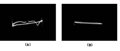
Fig. 7-32. Typical patterns obtained when the demodulator probe detunes an
i-f stage and throws it into oscillation. Since the scope deflection becomes
so small, an oscillating stage due to probe loading can easily be confused
with a weak or a dead stage.
The technician will find that various types of crystal signal-tracing demodulator probes produce varying degrees of distortion (of a horizontal sync pulse, for example). Although a demodulator probe which produces minimum wave form distortion may be preferred for signal-tracing work, such a probe may be rather disappointing when used to demodulate a visual-response curve, as the marker indication will be very broad. Accordingly, a demodulator probe which provides some degree of filtering at the scope input circuit will usually be preferred for visual-alignment applications.
(2) Stage-by-Stage I-F Signal Tracing. When the gain of the i-f amplifier is subnormal and cannot be restored by realignment, when the specified bandwidth cannot be obtained, or when regeneration or oscillation is present and the pro per response curve shape cannot be obtained, the technician often wishes to make a stage-by-stage signal-tracing check to localize the trouble in an i-f amplifier. The receiver is then energized at the antenna terminals by a suitable modulated r-f signal, or by a sweep-frequency signal, or by a sufficiently strong tv station signal. The signal should have the same frequency as the channel to which the tv receiver station selector is set. To trace this signal through the i-f circuits of the receiver, a demodulator probe and scope combination is applied successively to the plate terminals of the mixer, first, second, third and fourth i-f tubes, watching the pattern on the scope screen. If the pattern disappears at any point, the stage can be assumed to be dead (or oscillating), and trouble shooting is in order.
The type of pattern observed on the scope screen during signal-tracing procedures depends on the type of signal applied to the antenna terminals of the receiver. If a tv station signal is used as the signal source, the composite video signal will be seen on the scope screen. (A reasonably strong station signal must be used in order to obtain satisfactory scope deflection when testing early i-f stages, or a scope preamplifier must be used, because the signal level in the earlier i-f stages is relatively low.) If the signal source is a sweep-frequency generator, the frequency-response curve of the stage will be traced on the scope screen. For each of these signal sources, the height of the pattern from a zero volt baseline from one i-f stage to the next is a measure of the gain of that stage.
If a modulated r-f signal is utilized instead, the modulation waveform of the signal will be observed on the scope screen, and the height of this waveform from one stage to the next is a measure of the gain of that stage.
[[' For a comprehensive discussion of the alignment and signal-tracing of r-f, i-f and video amplifiers, see TV TROUBLESHOOTING AND REPAIR GUIDEBOOK, Vols. 1 and 2, by Robert G. Middleton, published by John F. Rider Publisher, Inc., New York, N. Y. ]]
The result of a stage-by-stage check may reveal a dead, weak, regenerative, or oscillating stage by the analysis methods outlined in Sec. 7-26 for such troubles. Occasionally, when a demodulator probe is applied to the grid or plate terminal of an i-f stage, little or no indication is obtained on the scope screen, despite the fact that the stage is not weak or dead. This situation may be the result of excessive loading of the stage by the probe, or may be the consequence of stage detuning which happens to throw the stage into oscillation, with the result illustrated in Fig. 7-32. When trouble of this kind is encountered and a low impedance type demodulator probe is not available, a conventional single diode probe, or a voltage-doubler probe, properly shunted as shown in Fig. 7-13 should be used. If the trouble still persists, a very small capacitor (approximately I µµf) should be connected in series with the tip of the probe to reduce the de tuning of the stage. A short length of 75-ohm 2-wire lead-in can serve as this capacitor. One conductor is connected to the test point while the probe is connected to the other conductor.
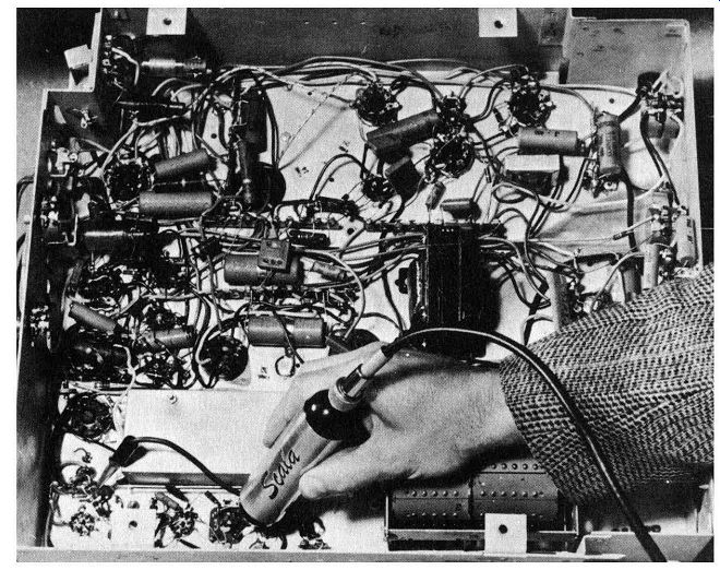
Fig. 7-33. Signal-tracing in a video i-f amplifier with a crystal demodulator
probe and scope. Observe that the probe ground-return is clipped to chassis
ground (at lower left) as close as possible to the signal take-off point. Courtesy:
Scala Radio Co.
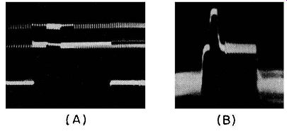
Fig. 7-34. (A) Display of de modulated composite video i-f signal obtained
when scope is connected via a low-capacitance probe at the output of the video
detector in a tv receiver. (B) Stripped appearance of the display of the demodulated
composite video r-f signal obtained when the scope is connected via a demodulator
probe at one of the video i-f amplifier stages. There is a definite reason
for the difference in the appearance of the two displays (see text).
(3) Importance of Proper Grounding of Demodulator Probe. Spurious scope patterns due to oscillation and other causes may also be produced in i-f amplifier alignment and signal-tracing work by the use of too long a ground-return lead to the demodulator probe, and most of the difficulty experienced by beginners is due to this cause alone. It should be remembered that this ground-return lead is part of the carrier-frequency circuit of the probe, and it therefore conducts current of carrier frequency. A demodulator probe with a moderately long ground lead is quite satisfactory for video-amplifier checking, where the highest carrier frequency to be accommodated is 4 or 4.5 mhz. However, for use in video i-f circuit work, where the operating frequency ranges from about 20 to 50 mhz, a short ground-return lead to the probe is essential (see Fig. 7-33). A parallel requirement is that the probe grounding connection be made as close as possible to the signal take-off point in the receiver, especially at frequencies above 100 mhz. Unless this is done, there may be spurious patterns due to ground-current effects at high frequencies. Those may take the form of consider able standing-wave voltage developed along ground leads, or even along a grounded metallic surface. Many technicians think they can dispense with the annoyance of progressively connecting and disconnecting the probe ground in i-f alignment or signal tracing work, simply by running a permanent ground lead from the scope case to the receiver chassis. In practice, a ground lead this long almost invariably causes erratic operation.
The matter of proper probe grounding is of great concern in r-f amplifier alignment and signal-tracing work when the signal source is of tv station frequency, since the carrier frequency may then be appreciably above 54 mhz. The accuracy with which tests can be made at these frequencies often depends on the way in which the demodulator probe is used. It is often found necessary to dispense with the short ground-return lead that is provided with the probe, and to make the ground return directly to the shielded case of the probe.
(4) Appearance of Composite Video Signal When Demodulator Probe is Used. The technician often finds it difficult to understand why the composite video signal looks different when viewed on a scope fed by a demodulator probe which picks the video signal off one of the video i-f amplifier stages, as compared with the appearance of the composite video signal when the scope is connected via a low-capacitance probe at the output of the video detector in the receiver (thereby employing the video detector as the demodulator in the test circuit). This difference is shown in Fig. 7-34, and there is a definite reason for it.
It might be supposed, for example, that a demodulator probe could be built with exactly the same circuit arrangement as is employed in a typical video detector, in order to obtain an excellent waveform of the demodulated video i-f signal. Unfortunately however, this demodulator probe would have to work into the scope input capacitance (including that of the scope cable), which is many times higher than the input capacitance of a video amplifier. The video-detector arrangement in a tv receiver, with its peaking coils, etc., works into the relatively small capacitance presented by the input grid circuit of the video amplifier; the demodulator probe, on the other hand, must work into as much as 50 to 100 µµF of cable and scope input capacitance. For this reason, it is unfair to expect the same demodulating ability from a simple, uncompensated demodulator circuit that works into a scope cable as from the more complex, compensated demodulator circuit working into the video amplifier in the receiver. In fact, if the bandwidth of a demodulator probe is excessive, the probe will not be useful for video-amplifier adjustment.
7-30. Demodulator Probe Application in Video-Amplifier Work
The video amplifier carries the actual picture or video frequencies, ranging from 0 to 4 mhz. In intercarrier receivers, it also usually carries the 4.5 mhz sound carrier signal. One method of effectively signal tracing, or checking the frequency response of, a video amplifier is by applying a sweep signal to its input circuit and displaying its output on the scope screen. The video sweep signal used in such tests usually varies from a low frequency of approximately 100 khz to 5 or 6 mhz, 60 times a second.
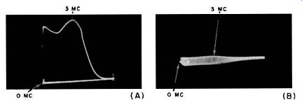
Fig. 7-35. (A) Response curve of a swept video amplifier as seen on the scope
screen when a demodulator probe is utilized and the scope vertical amplifier
is being employed. (B) Relatively small deflection obtained on scope screen
when the output of a swept video amplifier is applied directly to the deflection
plates of the cathode-ray tube in the scope.
No demodulator probe or scope vertical amplifier is employed. The video-frequency sweep voltage is displayed directly here.
Whether or not it will be necessary to use a demodulator probe with the scope depends upon the frequency-response characteristic of the vertical amplifier of the particular scope employed. A demodulator probe is not required for the response display when a wide-band scope is used, provided, of course that the scope has adequate sensitivity (see Fig. 7-35) and a flat frequency response out to well over 4.5 mhz. In this case, the sweep voltage is displayed directly. In the discussions which follow, it will be assumed that the limited frequency-response characteristics of the scope to be employed makes the use of a demodulator probe necessary. Because of its greater hum-voltage attenuation and better wave form-fidelity characteristics in this service, the shunt-rectifier type of demodulator probe is generally considered the most suitable for video-amplifier work.
(1) Sweep-Signal Testing of Video Amplifiers. The typical instrument setup for a frequency-response check, or signal-tracing, in a video amplifier by means of an applied sweep signal is shown in Fig. 7-36. The video detector is removed, or the grid capacitor to the first video amplifier is disconnected from the detector.
The demodulator probe is connected at the signal-electrode (usually the grid) terminal of the picture tube socket. The picture tube should. be removed from ...
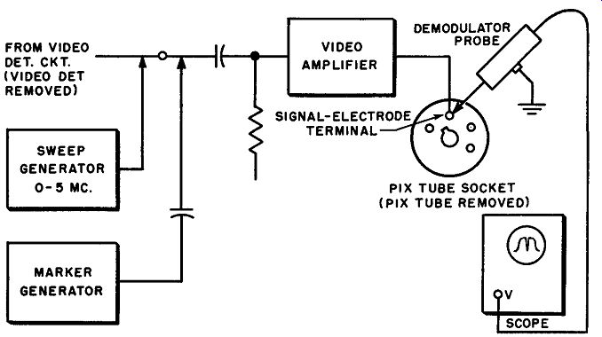
Fig. 7-36. Instrument setup for frequency-response check, or signal tracing,
in a video amplifier by means of a sweep signal, if the video detector is not
to be included. The demodulator probe used in this work must meet several important
requirements (see text).
... the socket so that the output circuit of the video amplifier is not loaded excessively during the test. This results in the first important requirement of the de modulator probe employed in this work, and is one reason why a demodulator probe which is satisfactory for video i-f amplifier signal tracing and alignment work may well be quite useless for video-amplifier work. The reason is that the frequency response characteristic of the video amplifier depends in great part on the shunt capacitance of the load connected across its output circuit, that is, upon the capacitance loading. If this shunt capacitance is appreciably greater than the input capacitance of the picture tube, the high-frequency response will appear to be very poor. On the other hand, if the shunt capacitance of the test circuit is appreciably less than the input capacitance of the picture tube, the frequency response will appear to be better than it really is when the receiver is in operation.
Obviously, the input capacitance of the demodulator probe used in this work should be approximately the same as the picture tube input capacitance, so that the capacitance loading on the output circuit will be the same as exists during normal operation of the receiver.
The probe must also have good response to 60-cycle square waves, because the demodulated sweep output is of the same general form as a 60-cycle square wave. If the time constant of the probe is too long, the scope will indicate a true rise, and a false fall, of the response curve.
The frequency characteristic of the demodulator probe is largely controlled by the value of the series isolating (filter) resistor which forms part of the probe filtering circuit. Unless this value falls within a suitable range to make the time constant of the filter suitable, a distorted reproduction of the video response curve will result, as shown in Fig. 7-37. The circuit constants shown in the de-modulator probe circuit in Fig. 7-9A are found to provide generally satisfactory probe operation in this work.
The video response curve produced by this test setup does not include the response of the video detector. If it is required to check the response of this circuit along with that of the video amplifier, a sweep generator and a single frequency r-f generator are employed to apply their signals ahead of the video detector. In this case, the two signals beat together in the video detector and produce a sweep output modulated in accordance with the response characteristic of the circuit under test. The output of the video amplifier is then applied through a demodulator probe to the scope.
----------
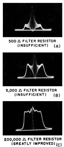
Fig. 7-37. The series filtering resistor in the output circuit of the demodulator
probe must have a value which makes the time constant of the filtering circuit
fall within a suitable range for the maximum rate of change of the signal that
will be encountered in the application. Otherwise a distorted response trace
will be obtained. (A) Filter resistor value much too low (time constant much
too short) for the application. This causes the scope to indicate a true fall,
but a false rise, in the actual video amplifier response, so a distorted response
trace results. The broad, fuzzy interference near zero frequency ( at the center
of the trace) is excessive unfiltered response displayed due to inadequate
filtering action provided by the probe output circuit. ( B) Less probe distortion
when a higher value of series filter resistance (longer time constant) is used.
(C) Greatly improved response curve when a resistance value close to the correct one for this application is employed.
If the time constant of the probe is made too long (by the use of too high a series filter - resistance value) the scope will indicate a true rise, but a false fall, in the actual video amplifier response.
500 FILTER RESISTOR (INSUFFICIENT) (A)
5,000. FILTER RESISTOR (INSUFFICIENT) (B)
200,000. FILTER RESISTOR (GREATLY IMPROVED) (C)
----------
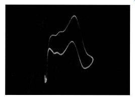
Fig. 7-38. Distorted video response trace obtained when a simple series-type
demodulator probe is used to demodulate the output sweep signal from a video
amplifier in which strong hum voltage is present. The hum distortion is seen
to be severe, and the time constant of the probe is excessively long for the
rate of change of the modulation envelope.
The results of a signal-tracing check of the video amplifier by the foregoing method may show a dead, weak, regenerative, or oscillating stage.
When making regeneration tests in video amplifiers, it is sometimes found that the available deflection on the scope screen is somewhat small, due to the fact that only one stage is being swept, and also because the output from the video sweep generator is attenuated by the isolating resistor which must necessarily be used. In such cases, it will be found that a voltage-doubler type of demodulator probe will provide approximately double the deflection on the scope screen, and thereby often facilitate the test considerably.
(2) Hum-Rejection Requirements for the Demodulator Probe. If 60-cycle or 120-cycle hum voltage is introduced into the test signal in some manner by the receiver, the visual response curve will be distorted accordingly. If a sweep signal having the customary 60 hz repetition rate is being employed, the trace and retrace will not lay over each other but will be displaced by an amount proportional to the hum voltage as it goes through its cyclic changes. The result is that distortion and displacement of the trace and retrace relative to each other occur. The resulting pattern (see Fig. 7-38) depends on the magnitude and the frequency of the hum voltage, and upon the phase relationship between the hum voltage and the test signal. It is evident that hum distortion in the video-amplifier response trace can be a troublesome problem unless a suitable type of de modulator probe which discriminates against 60-cycle or 120-cycle a-c hum voltage present in the signal to be displayed, is used with the scope. The shunt type of probe is generally found to have the best hum-rejection properties.
(3) Square-Wave Testing of Video Amplifiers. A square-wave test for video amplifiers is preferred by some technicians over the foregoing sweep-frequency test. This is true because the larger harmonic content of the square-wave test signal enables the amplifier characteristics to be checked over a wide frequency range, and also because it shows up important phase distortion as well as frequency distortion in the amplifier. A demodulator probe is not required in this test, but a wide-band scope must be used.
7-31. Demodulator Probe Application in Sound-Section Work
A d-c scope converts an a-m demodulator probe into an f-m peak-indicating probe. Therefore, an f-m demodulator probe, although practical, is not needed in troubleshooting or adjusting the f-m circuits of the sound section of a tv receiver (or of an f-m aural receiver). (1) Demodulator Probe Used to Develop Visible Marker for S-curve. The demodulator probe also finds useful application in ratio-detector work in the f-m section during sweep alignment of the tuned circuits. Because of the inherent a-m rejection by a properly operating ratio-detector circuit, it is often found difficult or impossible to distinguish the 4.5-mhz marker employed on the S-curve in this work. This situation is illustrated in Fig. 7-39A. The 4.5-mhz point on the S-curve can be easily located, as shown in part B of the figure, by applying the sweep voltage in parallel with the marker voltage, through a demodulator probe, into the vertical amplifier of the scope. The probe has no a-m rejection proper ties, so the 4.5-mhz marker now appears along the swept trace, as shown. By tuning the sweep generator, or by adjusting the horizontal centering control of the scope, the marker can be brought to the exact center of the screen, as shown in Fig. 7-39B, so that the vertical center line of the scope screen indicates the 4.5-mhz point. Next, the demodulator probe can be disconnected and the ratio-detector circuit placed in the test setup. Although the 4.5-mhz marker is now invisible, it is known that the point of intersection of the S-curve with the vertical center line of the scope screen marks the 4.5-mhz point on the S-curve.
Use of a voltage-doubler type general-purpose demodulator probe has an advantage in this application in case the marker voltage is quite weak, as the marker will appear a double-height on the scope screen when this type of de modulator probe is used (see Sec. 7-15). (2) Use of Demodulator Probe to Reveal Presence of Spurious Voltages. A d-c scope and a general-purpose demodulator probe make a useful combination for revealing the presence of spurious voltages in the f-m sound system. For example, it may be used to reveal any modulation which may be impressed on the 4.5-mhz f-m sound signal by the picture signal (mainly by the vertical sync pulse) during the course of passage of the signals through the video i-f circuits. The resting position of the scope beam is first noted on the screen before any signal is applied. Next, the f-m sound signal just ahead of the ratio detector is applied to the demodulator probe, and the sound signal pattern appears on the scope screen, rising above the zero-volt level by an amount which is determined by the d-c component of the signal. This in turn is determined by the percentage of the modulation. The latter is measured directly from the pattern. If its value is more than about 35 to 40 percent, trouble should be sought in the video i-f circuits, or possibly the video amplifier circuits, before the sound circuits are investigated.
It is sometimes observed during such tests, that the scope trace appears at some distance above the zero-volt level when the demodulator probe is applied to the sound circuits under test and no sound signal is present. The deflection in this case is due to spurious voltages present in the amplifier, which may be caused by internal or external interference. The possibility of external interference entering the receiver can be checked by switching to other tv channels, or by removing the video-detector tube.
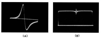
Fig. 7-39. (A) A ratio-detector S-curve is often difficult to mark because
the a-m rejection of the ratio-detector circuit rejects the beat marker. (B)
A general-purpose de modulator probe may be used to make the 4.5-mhz marker
visible on a separate swept trace, thus calibrating the horizontal baseline
of the scope.
The marker may be made to appear at the exact center of the screen, as shown.
Internal interference is usually caused by some form of oscillation in the sound amplifier or video amplifier, or both. Tubes can be removed progressively, to find out which stages are involved, or a bypass capacitor can be shunted from the grid of each tube, in turn, to ground. The shunting method breaks the feed back path, and causes the scope trace to drop to the zero-volt level.
(3) Buzz-pulse Tracing in the Sound I-F Amplifier. A scope, together with a conventional general-purpose demodulator probe of the type illustrated in Fig. 7-9, or a voltage-doubler type as in Fig. 7-18, can be used to view trouble some 60-cycle buzz voltage that may be present in the 4.5-mhz f-m circuits of the sound amplifier, in order to localize it to its origin. The circumstance leading to the production of the buzz pulses determines the appearance of the waveform.
When the 4.5-mhz sound signal is displayed on the scope screen, excessive buzz voltage in this circuit will become apparent as a 60-cycle pulse which usually has a vague resemblance to the vertical sync pulse from which it is derived (see Fig. 7-40). This occurs in the case of tunable buzz. In the case of un-tunable buzz, the pulse more often appears as a sharply pointed 60-cycle spike voltage.
Buzz problems are frequently difficult to solve, because there are a large number of points in a receiver where buzz pulses may originate and be introduced. Tuned heads are required in conjunction with the demodulator probe when checking for buzz in circuits that normally carry picture signals.
(4) The Demodulator Probe Should be Applied in Low-Impedance Circuit.
It is always advisable to apply the demodulator probe in a low-impedance circuit in the sound i-f amplifier or ratio-detector circuit. If the receiver does not afford low-impedance test points, it is practical to insert a resistor having a value of 5 or 10 ohms between the cathode of the tube being tested and chassis. The small voltage drop across the resistor has no practical effect on the circuit operation, but provides enough signal voltage for full-screen deflection on a sensitive scope. The blocking capacitor in the demodulator probe blocks off the d-c drop, but passes the spurious a-c voltage which is then demodulated for display on the screen of the d-c scope.
7-32. Special Demodulator Probe to Test for Presence of Spurious Voltages in Heater Lines
The technician will obtain much additional utility from demodulator probes if he is alert to the possibility of special applications for them. For example, difficulty in receiver operation is sometimes encountered because of feedback of high frequency voltages through heater lines. Direct application of the scope to the heater line in order to detect or study such spurious voltages cannot be resorted to because the vertical amplifiers of conventional service-type scopes usually do not respond to the high frequencies ordinarily involved in this type of trouble.
Also, the 60-cycle heater voltage which is present, is not appreciably attenuated with respect to the high-frequency spurious voltage which is being sought. It will be found that direct application of the scope merely displays the 6.3-volt a-c heater voltage.
For a comprehensive discussion of the causes, and the methods of tracing, the origin of buzz pulses in a tv receiver, see TV TROUBLESHOOTING AND REPAIR GUIDEBOOK, Vol. 1, Section 9 by Robert G. Middleton, published by John F. Rider Publisher, Inc., New York, N. Y.
Fig. 7-40. Appearance of a 60-cycle sync-buzz pulse at the input of the ratio-detector circuit. Display obtained by using demodulator probe and a-c scope. If a d-c scope is used, the d-c component in the signal output from the demodulator probe is utilized.
However, when a demodulator probe is used in the test, (especially if it employs a relatively small value of series capacitance) it greatly attenuates the 60-cycle component, and the demodulation action of the probe develops the wave envelope of the high-frequency spurious voltage, which then becomes visible upon the scope screen. In most checks of this type, the attenuator of the service scope must be advanced to maximum gain, or a pre-amplifier must be used. Use of a voltage-doubler type demodulator probe is especially useful in this work, because of its high sensitivity. If the heater-bypass capacitors open up, or if the r-f chokes in the heater string become shorted, or are improperly dressed with respect to other components, spurious voltages will increase in value, and cause obscure difficulties in receiver operation. The demodulator probe and scope, accordingly, serve to provide definitive answers to the cause and location of such troubles in case the heater string falls under suspicion.
When testing for the presence of spurious high-frequency voltages in heater lines and similar circuits in this manner, it is desirable to obtain a high degree of 60-cycle hum-voltage rejection in the demodulator probe employed, so that the hum-voltage trace will not interfere with the high-frequency wave-envelope trace. Hum rejection is greatly increased by the use of a small value of series capacitor in the demodulator probe, and special probes may be shop-constructed with this feature exaggerated for this particular type of work. The voltage doubler probe shown in Fig. 7-41 is of this type. (Compare the relatively small value of series capacitance used in it with the much larger value employed in the general-purpose voltage-doubler demodulator probe shown in Fig. 7-18.) The same method of probe design can be used to obtain square-wave rejection when testing the output from a simple square-wave modulator.
7-33. Demodulator Probe Use in Marker and Signal-Generator Checking (1) Marker-Generator Accuracy Check. Questions frequently arise concerning the accuracy of a marker generator. If a crystal oscillator is available (some sweep generators have a built-in crystal oscillator), this can be used with a 1- or 2-mhz crystal, a sensitive demodulator probe, and a scope, for calibration of the marker generator. The output from the marker generator is paralleled with that from the crystal oscillator. The mixed outputs are applied to the demodulator probe which feeds into a scope that is being internally swept at any convenient low-frequency rate, such as 60 cycles. Although the frequencies of the signals from the marker generator and oscillator are too high to affect the scope directly, the demodulator probe develops a beat envelope which will be visible on the scope screen.
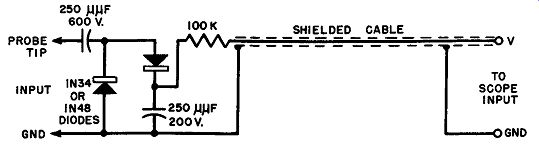
Fig. 7-41. Special shop-constructed voltage-doubler demodulator probe designed
to have a high degree of 60-cycle voltage rejection due to the small size of
series capacitance employed in it. This type of probe is extremely useful for
localizing spurious high-frequency voltages in 60-cycle a-c heater lines.
As the marker-generator frequency is changed so that a beat is produced that is within the frequency range of the scope, some vertical deflection occurs and the waveform of the beat note appears on the screen. Therefore, as the marker-generator frequency is varied through the frequency of the crystal oscillator (or its harmonics), the difference frequencies and the zero-beat produced in the probe circuit are clearly visible on the scope screen. In this manner, calibration of the marker generator is made possible. If a 2-mhz crystal is used, beats will be encountered at 2 (strongest), 4, 6, 8, 10 ... 30 mhz. Above 30 mhz the harmonics will usually be rather weak for practical application, although use of a voltage-doubler type demodulator probe in this work will enable the opera tor to work further out on the harmonics from a given crystal oscillator since this type of probe gives approximately double the deflection on the scope screen as is provided by a conventional single-diode probe.
(2) Calibrating a Signal Generator at 4.5 mhz. A conventional signal genera tor may be calibrated accurately at 4.5 mhz to be used as an accurate marker source for sound-detector alignment, although a calibrating crystal oscillator may not be available. Mix the input to the sound detector in a tv receiver that is receiving a station signal, with the output of the signal generator, and apply the beating waves to a pair of earphones through a demodulator probe. The strongest component on the sound-detector input is the 4.5 mhz sound carrier, and an easily distinguishable beat note will be heard as the signal generator is tuned through 4.5 mhz. In this manner, the signal generator may be calibrated accurately at 4.5 mhz.
(3) Checking Output of a Signal Generator for Presence of Hum Voltage.
The presence of hum voltage in the output of a signal generator is usually very objectionable. It appears as either a simple mixture of 60-cycle hum voltage with the r-f voltage, or as a modulation of the r-f voltage by the hum voltage. Either type of hum can be displayed and measured on a scope screen, but different test arrangements must be used for the two conditions, as shown in Fig. 7-42. Observe that a crystal diode is used in the second arrangement, and it is inserted at approximately the middle of the shielded connecting cable.
(4) Demodulator-Probe Crystal Polarity. When testing the output from a test oscillator, or a signal generator, with a single-diode type demodulator probe and scope (or vtvm), it is often found that the indicated voltage differs considerably when the crystal diode is reversed in polarity. This difference of indication with reversal of the crystal in the probe is an indication of even-harmonic distortion in the generator output voltage (see Sec. 7-23 and Fig. 7-25). Although the presence of even-harmonic distortion is easily revealed in this manner, the presence of odd-harmonic distortion must be determined by other means. A field-strength meter tuned to the frequency of an odd harmonic can be used to measure the odd-harmonic output voltage.
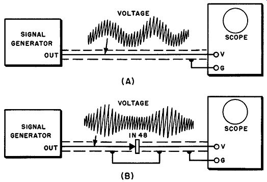
Fig. 7-42. Methods of displaying and measuring hum voltage appearing in the
output of a signal generator. (A) Test setup if the hum voltage appears as
a simple mixture of the hum voltage and the r-f voltage. (B) Demodulator test
setup required if the hum voltage is modulating the r-f output voltage of the
generator. The modulated r-f voltage is demodulated by a crystal diode, and
the hum-voltage envelope is displayed on the scope screen. In either check,
the hum voltage appears as a 60-cycle sine-wave pattern on the scope screen.
7-34. Demodulator Probe Use in Checking Sweep-Signal Generators
(1) Checking the Flatness of Output. One type of sweep-generator fault which is serious in most applications of such generators concerns an output signal which contains some amplitude modulation. In this case, the amplitude of the output varies as the frequency is swept over the sweep range.
The service technician may check the amplitude of the sweep generator output by using a demodulator probe to demodulate the output of the sweep generator, and applying the probe output to a scope. If there is no variation in the sweep generator output over the frequency range through which it is being swept, then a perfectly straight horizontal line appears on the scope screen, as shown in Fig. 7-43A. (A high gain-setting should be used on the scope for this check.) If a sloping line is produced as in part B of the figure, or if a line occurs which has peaks or valleys along its length as in part C, then the sweep generator has an output whose amplitude is not constant over the range of frequencies being swept. If such an output sweep signal is used for checking the frequency-response characteristic of an amplifier, a false response trace will be obtained.
For ordinary service work, the output voltage from a sweep generator should be flat within approximately plus-or-minus 10 percent over the swept band.
Some sweep generators are blanked during retrace so that no output is produced during this time. In this case, two horizontal lines appear on the scope screen if the amplitude of the generator output is constant (see part A of Fig. 7-43). One of these lines represents the demodulated output of the generator during the active time, while the other represents the zero output of the generator during retrace time (it is actually the zero-level trace).
Fig. 7-43. Typical patterns obtained when checking the flat ness of the sweep-signal
output from sweep generators by means of a demodulator probe and a scope. (A)
Reasonably flat output over the swept range. (B) Output slump-off at one end
of the swept range. (C) Output with very bad slump-off at mid-sweep region.
In all cases, sweep-generator blanking was employed to produce the zero-volt baseline.
A note of caution on the use of this method is that the response of the demodulator probe employed may not be uniform within the frequency range being checked. Under these conditions, the type of pattern shown in Fig. 7-43B might be the result of the response of the probe falling off at the high frequencies, rather than the output of the sweep generator falling off. Also, the probe and-cable may have resonance effects at various frequencies within the swept range. Under these conditions, the peaks or dips in the pattern shown in Fig. 7-43C might be the result of these resonance effects.
To check this, construct several different demodulator probes (or check several commercial varieties of demodulator probes if possible). The various probes should be constructed using different components and crystal diodes, but of course with high-frequency capacitors and composition resistors. Also the probe components should be properly isolated from the input cable. The mechanical arrangement should be varied slightly, and different shield housings can be tried. The effects of these changes on the scope pattern produced should be noted in each case. If two or three probes are found to give substantially the same pattern on the scope screen, and if the outside of the cable is "cold" the technician can be reasonably certain that the probe is satisfactory, and that the output cable termination and r-f ground lead are satisfactory.
Fig. 7-44. (A) Suitable arrangement for checking flatness of the output of
a single-ended sweep generator. The sweep-generator cable termination shown
in the diagram has a value of 75 ohms; in some cases, the cable termination
should be 50 ohms, and in still other cases, 100 ohms. The requirement is for
the cable termination to match the characteristic impedance of the cable. (B)
Suitable arrangement when sweep-generator has double-ended output. In this
example, the generator is intended to work into a 300-ohm load. The 300-ohm
load is a pair of 150-ohm resistors connected in series to provide a center-tap
for the ground-return of the demodulator probe. Resistors R1, R2, and R2, are
usually provided by the sweep-generator manufacturer, and serve to match a
300-ohm load to the characteristic impedance of the output cable.
The output flatness test should not be employed at the higher frequencies provided by the sweep generator, since misleading results are more likely to be obtained due to the likelihood of poor high-frequency response and the presence of resonance effects in the probe at these frequencies. For example, a voltage doubler type probe which is reasonably flat up to 80 or 100 mhz should not be used to check a sweep generator operating above this frequency. A single-diode demodulator probe which is reasonably flat up to about 200 mhz should be used only below this frequency in the test.
The basic circuit arrangements for making this test arc shown in Fig. 7-44.
When the sweep generator has single-ended output, a simple single-ended shunt-type demodulator probe arrangement which is flat up to about 200 mhz is utilized as shown in Fig. 7-44A. When the sweep generator has double-ended output, a double-ended demodulator probe similar to the one shown in Fig. 7-16A is used, as shown in Fig. 7-44B. When testing the output from sweep generators where the grounding system is slightly "hot", with the result that the shape of the scope trace changes every time the operator changes his position or grasps the generator output cable, it is often of considerable assistance in stabilizing the. test setup to partially isolate the demodulator probe from the sweep-generator output cable termination by means of a 125-ohm composition-type series resistor connected at point X in each of the demodulator input leads as shown in the diagrams.
It should be recognized that these test arrangements are most useful when the output from the sweep generator is a pure and unmixed output. Some caution should be observed when checking the output from very simple types of beat-frequency type sweep generators, since their output is often a mixed output comprising feed-through frequencies from the beating oscillators, sum-and-difference beat frequencies, and harmonics of these frequencies.
When used to align a receiver, the receiver tuned circuits reject the unused frequencies in the output of the generator, but a demodulator probe applied directly to the sweep-generator output will necessarily accept all frequencies present. In consequence, the output flatness check using a demodulator probe and scope will not necessarily provide a check of the output voltage for only those frequencies which the setting of the dial of the generator would indicate.
Output voltage of other frequencies may be present also and is recorded on the scope. Under such circumstances, the flatness check is not necessarily valid un less the operator utilizes suitable output filters to remove the unwanted frequencies.
It is quite possible, for example, for the fundamental output from a sweep generator to be quite flat, while the second-harmonic output may be far from flat, due to partial resonances in the output system. For this reason, the operator should be certain to study the circuit diagram of the sweep generator before tests are made, and to provide suitable filters, if required. Sometimes low-pass filters are built into the generator, and sometimes they are provided as accessory units. In other cases, the technician will have to make use of 75-ohm or 300-ohm filters (as the case may be) which have been designed primarily for other applications.
The technician sometimes falls into the error of assuming that because a sweep generator is flat on a fundamental frequency, it must also be flat on the second harmonic, or on the third harmonic. This is not true, because it is very possible for residual resonances to impair the flatness of the output on a harmonic, while leaving that on the fundamental unaffected. In other words, when the flatness of a sweep generator is being checked by means of filters to remove all frequencies but one (swept band) from the output, it cannot be assumed that because the difference output is flat, that the sum output must also be flat, or that because a fundamental output is flat, that the harmonics of the fundamental output are flat. Independent checks must be run on each of the mixed frequencies present in the output of the instrument.
(2) Checking the Sweep Width. When it is desired to check the sweep width of a sweep generator that is to be used for i-f alignment, connect the output cable from the sweep generator in parallel with the output cable from a marker generator. Next, feed this combined output through a demodulator probe to the scope. The sweep-generator output display (see Fig. 7-43), having the marker superimposed at some point, will be observed. Then tune the marker generator to run the marker from one end of the sweep-generator trace to the other. The difference between the two indications on the marker-generator dial for these two extreme positions of the marker is the sweep width.
7-35. Use of Demodulator Probes with VTVM's
Conventional-type demodulator probes, such as those shown in all illustrations preceding Fig. 7-17 in this section, may also be used with a vtvm. When the output of such a probe is applied to any vtvm set to its D-C Volts position, the scale indication is proportional to the average amplitude of the r-f a-c carrier voltage, or of the modulation waveform, of the modulated signal applied to the probe. When used with a peak-indicating, or a peak-to-peak indicating, a-c vtvm set to its A-C Volts position, the scale indication is proportional to the peak voltage of the modulation waveform of the signal under test, because the de modulator probe rectifies the voltage under test before it reaches the vtvm.
When the output from a voltage-doubler demodulator probe is applied to any vtvm set to its D-C Volts position, the scale indication is proportional to the numerical sum of the positive and negative values (peak-to-peak value) of the r-f a-c carrier voltage of the modulated signal applied to the probe. When the probe output is applied to either a peak-indicating, or a peak-to-peak indicating, a-c vtvm set to its A-C Volts position, the scale indication is proportional to the peak-to-peak voltage of the modulation waveform of the signal under test.
A crystal demodulator probe introduces an insertion loss in the circuit to which it is applied. The loss of signal voltage encountered varies considerably, but is typically of the order of 5-to-1 in a single-rectifier type probe. Consequently, demodulator probes are generally designed to be used as indicating rather than as measuring devices. If it is desired to use a demodulator probe as a measuring device, it is necessary to calibrate it for the scope or vtvm with which it is to be used, by first checking the indication of the vtvm or scope when a known source of peak, or peak-to-peak, voltage is applied to the probe input, in order to determine the attenuation factor of the probe. Since the front-to-back ratios of various crystal diodes are different, demodulator probes must be individually calibrated for insertion loss with the particular vtvm or scope they are to be used with whenever they are to be used as voltage-measuring devices.