A number of special circuits have been developed to aid the use of TTL in various applications. Many of these circuits fall into the category of interface circuits, since they allow TTL to work into or from other types of electronic circuits, including digital logic families and analog or linear circuits.
INTERFACE DRIVER
Linear IC, type 75450, is a dual peripheral driver consisting of two NAND gates and two isolated transistors ( Fig. 10-1A). The transistors are rated at 300 mA continuous collector current, and the NAND gates require the usual +5-volt supply.
The IC can be used to drive two lamps or two relays, each connected as shown in Fig. 10-1B. When the gate is low, the transistor is off and the load is connected to ground through a very high impedance. When the gate is high-which requires at least one input to be a 0-the transistor is on and the load is connected to ground through a very low impedance. Current then flows through the load from +V to ground. The diode suppresses transients when the transistor is turned off.
Two type 75450 devices can be used to drive an ac load as shown in Fig. 10-1C. To operate as an ac source, the A transistors are turned on together while the B transistors are held off. Then, the A devices are turned off and the B transistors are turned on, and so forth.
If any possibility exists that an A and a B transistor can be on simultaneously, current-limiting resistor Ill must be made large enough to keep the transistors from burning out. If the load is inductive, the circuit must be analyzed to prevent turn off transients from destroying the transistors.
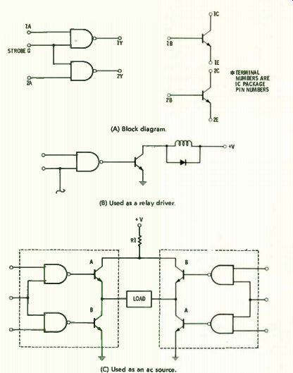
(A) Block diagram. (B) Used as a relay driver. (C) Used as an ac source.
Fig. 10-1. Dual peripheral driver.
ONE-SHOT MULTIVIBRATOR
Sometimes one pulse must be delayed, relative to another, to prevent improper operation of a circuit. In other cases, a signal source does not generate pulses as such, but the information obtained from the source is required in the form of pulses.
Sometimes pulses need to be lengthened or shortened to be compatible with other signals. The one-shot multivibrator shown in Fig. 10-2A can be used for these functions.
Operation is straightforward. With either A1 or A2 low and B high, a single positive-going pulse is generated at Q. Typically, the width of the pulse is 30 nanoseconds but can be increased to as long as 40 seconds by adding a resistive-capacitive timing circuit as shown in Fig. 10-2B.
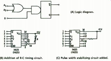
(A) Logic diagram. (B) Addition of R-C timing circuit. (C) Pulse width stabilizing
circuit added.
Fig. 10-2. A one-shot multivibrator.
The value of capacitor C can vary from 10 pF to 10 µ,F, and the value of resistor R can range from 0 to 40,000 ohms. Pin 9 is connected to an internal resistor of about 2000 ohms, and this resistance is in series with the external resistor. The connection shown in Fig. 10-2C stabilizes the width of pulses generated by the one-shot multivibrator.
Fig. 10-3 shows the pulse lengths that can be obtained for various values of C and R. With C = 1 uF and the total timing resistance (the sum of external R and internal 2K resistor) = 10K, the curve shows a typical pulse width of 7 milliseconds.
LATCHES
One major use of latches is as a temporary storage of data between a data source and an indicator. If the input to an indicator (such as a 7-segment readout tube) changes more than a few times a second, the result is an unreadable flicker.
By storing the information temporarily, thus keeping the indicator from changing more often than once or twice a second, useful and readable outputs are obtained (although some inter mediate readings may be lost). Fig. 10-4A shows a one-bit latch that is incorporated in a 4 bit bistable latch (circuit types 5475/7475 and 5477/7477) and in an 8-bit bistable latch ( circuit type 54100/74100) . The major differences between the ICs are the internal clock connections and the available outputs. Circuit type 5475/7475 has both Q and 711 outputs for each of four latches, while type 5477/ 7477 and type 54100/74100 have only Q outputs.
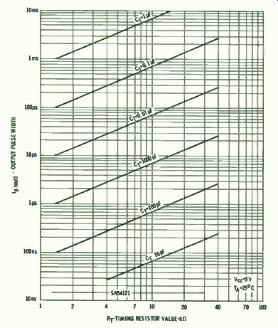
Fig. 10-3. Typical characteristics.
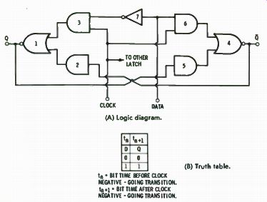
Fig. 10-4. One-bit latch.
Whenever the clock is high, the information on the data input appears on the Q output and Q will follow the data.
When the clock goes low, Q no longer follows the data but stays in its last state.
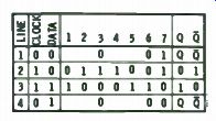
Fig. 10-5. Analysis table for Fig. 10-4.
In the analysis table ( Fig. 10-5) , line 1 shows both the clock and data low. This causes Gates 3 and 6 to be a 0 and, thus, NOR Gates 1 and 4 will be determined by prior conditions. Line 2 shows the clock high and data low. Gate 3 is now high and this drives Gate 1 to 0. The other gates follow as shown in the analysis table; Q goes to 0; Z1 goes to 1. In line 3, both clock and data are high. Now Gate 6 is high; this drives Gate 4 to a 0, and the other gates are driven to the conditions shown. In line 4, the clock is 0 and data is 1. Again, Gates 3 and 6 are low, and the circuit remains in the state it was in when the clock went low.
Prev: MEMORIES
Next: INCREASING TTL SPEED AND DEVICE DENSITY
Guide Index : Transistor-Transistor Logic (early 1970s)