Three basic types of memory functions have been developed so far in TTL. The first type is the random-access read-write memory. It is similar to a magnetic core memory, since you put data into the memory on command and then read it out as required, one word at a time. The second type is called a read only memory. In this type circuit, the information is put into the circuit at the time it is manufactured and cannot be changed thereafter. This type of memory is very useful for storing data that does not change with time, such as trigonometry tables, code conversion schemes, and microprograms for computers. A third type memory is called an associative or content-addressable memory. A major advantage of this type memory is its speed of response when searching for information.
A memory must perform three functions. First, it must provide a way for information to be put into it. Its contents may be changeable in a read-write memory and fixed in a read-only memory. Second, it must retain the information stored in it.
Finally, it must deliver the information when asked for it.
Very small memories are sometimes organized to store single bits of information. Thus, a 16-bit memory has 16 different locations for storing a bit. Each location is isolated and independent of every other location. If you want to know whether bit location 12 is holding a 1 or a 0, you have to ask the memory the equivalent of, "What information is in position 12?" In order to single out bit position 12, an addressing scheme is needed that will allow bit 12 to be interrogated without disturbing the other locations. An address scheme is also required when information is loaded into bit 12.
Large memories are usually organized in terms of words rather than single bits. Circuit type 5488/7488 (a high-speed monolithic IC) is organized as 32 words of 8 bits each. It is a 256-bit read-only memory but its contents are available only as 32 different words. Thus, instead of having to address 256 different bit locations, only 32 word locations have to be ad dressed. The addressing scheme is much simpler.
The major advantage of semiconductor memories over magnetic core memories has been operating speed. Semiconductor memories operate as much as 100 times faster than core memories. Core memories, on the other hand, cost less than semiconductor memories. Thus, many systems today use large, relatively slow core (or magnetic tape, disc, etc.) memories for storing large masses of information. Small fast semiconductor memories are used for temporary storage of information that is being processed. A major disadvantage of semiconductor memories is that they will lose the information stored in them when power is lost-the memory is said to be volatile since the information vanishes when the power is cut off. This does not apply to read-only memories. They hold their information whether the power is on or off.
RANDOM-ACCESS MEMORY (RAM)
Fig. 9-1 shows the arrangement of the 16-bit active-element memory, circuit type 5484/7484. The storage section consists of 16 flip-flops arranged in a 4-by-4 matrix. Each flip-flop can be addressed by energizing one of the 4 X-input lines plus one of the 4 Y- input lines. By using a matrix arrangement, the address function requires only eight inputs, instead of the 16 that would be required if each flip-flop had its own input address line. As the number of bits in a memory increases, the matrix scheme becomes more and more efficient: a 64-bit memory needs 8 + 8 or 16 inputs rather than 64; a 256-bit memory needs 16 + 16 or 32 inputs rather than 256; etc.
Data does not enter the memory via just one input, however, but is entered via a "Write 1" and a "Write 0" input. Similarly, the outputs are obtained from a "Sense 1" and a "Sense 0" amplifier.
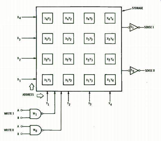
Fig. 9-1. RAM storage arrangement diagram.
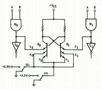
Fig. 9 - 2. Schematic of a storage flip-flop.
A storage flip-flop is shown at Fig. 9-2. In normal storage operation, assume the flip-flop is holding a 0, and, therefore, transistor Q. is on (saturated). Then, its collector and the base of transistor Q1 will be low, causing Q1 to be off, and its collector and the base of transistor Qo to be high. Inputs for writing will all be low and, thus, Gates W o and W, will be high, causing emitters Eo and E, to be high. The current flowing through transistor Qo will flow out the X0 and Yo lines, which are both grounded. The outputs of the sense amplifiers will be high.
To read the state of a bit, the X and Y address lines are brought to a 1. If only the X emitters are brought high, the current that was flowing out of X,, and Yo flows out of emitter Yo only. Similarly, if only Yo is brought high, the current flows
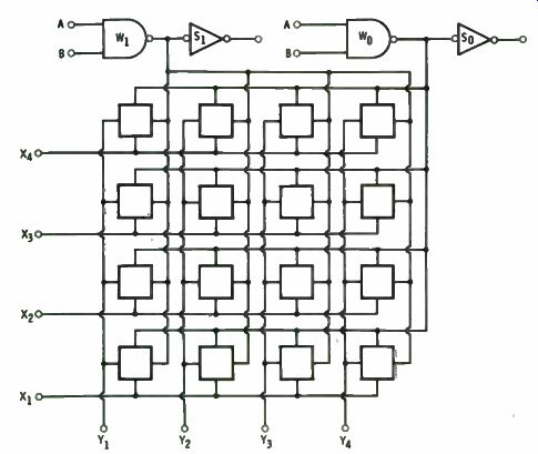
Fig. 9-3. Typical c ction diagram of a RAM. out of emitter Xo. In either case,
the status of the circuit stays the same. But when both X and Y emitters are
brought high, the current is diverted into the E„ emitter and flows into the
input of gate S 0. The result is that the output of the " Sense 0" amplifier
falls to 0. The "Sense 1" amplifier is not affected and its output
stays high. For the conditions where the flip-flop is storing a 1, Q, will
be the saturated transistor; when X and Y are brought high, the current from
E, causes the " Sense 1" amplifier to go to 0, while gate S o stays
high.
Suppose that bit location X,,Y, is to be interrogated. When address lines X3 and Yo are brought high, all the flip-flops in row X3 have their X emitters raised, while all the flip-flops in column Y2 have their Y emitters raised. Only the flip-flop at X3Y2 has both the X and Y emitters raised. Thus, only it acts on the sense amplifiers and only one sense amplifier goes low.
To write data into the flip-flop at X3Y2, the X3 and Y2 address lines are brought high, as in reading. To write a 0, both inputs of the "Write 0" gate are brought high, which drives Wo to 0. If Q0 is already on, nothing changes. However, if Q0 is off, the potential of Eo falls sufficiently below that of El so that transistor Q0 turns on and transistor Q1 turns off. This action occurs because the sink impedance of Wo, when low, is less than the input impedance of S 1. Once the flip-flop has taken on the desired state, it remains there after address and write inputs are brought low. Writing a 1 into a flip-flop is the same as above, except that the Write 1 amplifier is used, and transistor Q1 is driven on.
When writing in a 1 or 0, only the flip-flop that is addressed is affected. In all the other flip-flops, the low X and/or Y inputs prevent the Write amplifier from changing the state of the flip flop.
A memory very similar to the type 5484/7484 memory just described is circuit type 5481/7481. It has only one input to each write amplifier; thus, it does not require an additional gating or clocking signal.
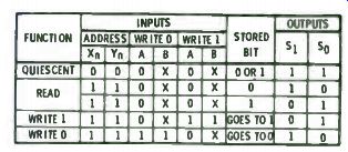
Fig. 9-4. Function. table for Fig. 9-1.
REGISTER FILE
In very high speed systems, it is often desired that the con tent of a memory be available even while new information is being entered. Fig. 9-5 shows a high-speed buffer memory (4-by-4 register file) that allows simultaneous reading and writing.
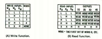
This buffer memory (circuit type 54170/74170) is organized into 4 words, each 4 bits long. Word 1 is stored in the 4 flip flops ( actually, latches) in the left column; word 2, in the next column; and so forth. The memory has two address systems, one for writing and one for reading. The address systems consist of a 2-bit code plus an enable signal. The Write address system consists of code W AW B and enable Gw. For example, to write new data into word 1, WA, W B and Gw are brought low.
(See the Write Function truth table.) This drives Gates 49, 50, and 47 high, and the latches of word 1 respond to the data on inputs 1D through 4D. If input 1D is a 1, then the latch for bit 1 of word 1 goes to Q = 1; if input 1D is a 0, the latch goes to Q 0.
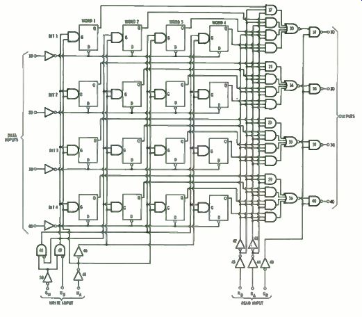
Fig. 9-5. Functional block diagram for a Register File.
Let the Write Function advance to word 2 and readout the contents of word 1 at the same time. To select readout of word 1, Read inputs RA, RB, and GB are brought to 0; this applies two is to Gates 17, 21, 25, and 29. If bit 1 of word 1 is a 1, Gate 17 turns on. Gate 33 then has two inputs 0 and one input a 1. Its output is 0. The output gate ( 37) has one input of a 1 ( from GB = 0), but, since the input from Gate 33 is a 0, the output 1Q is high. Similarly, if Q1 = 0, the signal will propagate through the read-address system and appear at the output as a 0. The other three bits of word 1 appear at the outputs in the same manner.
Thus, the memory is seen to operate somewhat differently than the 16-bit memory considered previously. The data appears on only one output, instead of two; it appears in true form, rather than in complementary form; it appears in groups of 4-bits at a time, instead of as single bits. With this
(A) Write function. (B) Read function.
Fig. 9-6. Truth tables for Fig. 9-5.
memory, reading of any word can occur simultaneously with the writing of any word ( including the word being written) ; whereas in the previous memory, only the bit being written in could be read out simultaneously.
READ- ONLY MEMORY (ROM)
Read-only memories tend to be larger in terms of storage capacity than random-access memories. This characteristic follows naturally from the fact that no write-in circuits are required. All that is needed is an address system and an output circuit.
Most ROMS are designed to fill the specific needs of one circuit and, usually, one customer. Thus, they are special circuits, rather than standard off-the-shelf devices. Once the customer decides what information the ROM has to store, he transmits this data to the IC manufacturer. The manufacturer creates a special photo-mask that contains the data and uses it as the final masking step in manufacturing the ICs. The process is relatively expensive if only a few ICs are needed but becomes less expensive when the cost is spread over a few hundred or more ROMs.
Certain types of stored information are useful in more than one application, so a few standard ROMs have been developed to meet these needs. Code conversions, reference tables, and display and readout systems may be able to use standard ROMs.
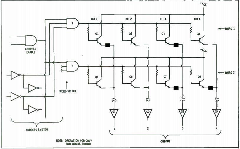
Fig. 9-7. Operating principle of a Read-Only memory.
The operating principle of a ROM is very straightforward and is shown in Fig. 9-7. Only two words are shown, each 4 bits long. Assume the address system has selected and enabled word 1 and, therefore, Gate 1 is high. As a result, the bases of all the storage transistors of word 1 are high. The square block in the emitter circuit of bit 1 is a metal connection that allows the circuit of the transistor to be completed and, thus, current will flow through transistor Q1. This current into Gate S1 causes S 1 to go high. For bit 2, the connection between the emitter of transistor Q2 and the input of Gate S2 has been removed, and Gate S2 stays at 0. Similarly for bit 3 ( S 3 = 1) and bit 4 ( S 4 = 0) . The transistors of word 2 are also connected to the output amplifiers, but, since the bases of these transistors are low, no current flows even when the emitter is left connected. When word 2 is selected and enabled by the address system, the output changes to the pattern set into the ROM for word 2. For manufacturing reasons, the ROM is made initially with all links in place. The ROM is customized to a specific application by removing links for those locations where 0s are desired.
Various types of organizations are available in ROMs. Fig. 9-8A shows a 32-word by 8-bit ROM, monolithic type 5488/ 7488. Operation is very straightforward. Simply apply the address code (see word select table) of the desired word, put the enable low, and read out the data.
CONTENT ADDRESSABLE MEMORY
Some systems require what can be called a searching operation or function. Suppose a system is being used to monitor aircraft entering and leaving the airspace of a landing field.
The display system for the tower operator includes a cathode ray tube (crt) on which he can call up information about all planes in the area. He may, for example, want a display of all planes flying at a certain altitude. Or, he may want a display of all planes that are within a 10-mile radius of the landing strip.
Each plane will have its own identification number and will be represented by a digital word in the monitoring system. The word may be sectioned, as indicated in Fig. 9-9A, where a certain group of bits provide plane identification; another group of bits give the altitude of the plane; another group, its distance from the field; and so on. As the plane moves through the area, the information is continually updated by various radars and transponders.
Assume the control tower operator wants to check all planes at altitudes from 5000 to 6000 feet and that the digital word representing these altitudes is 1101. One way to do this would be to check the digital words associated with all the planes in the area to see if their altitude field is 1101. Any plane having the altitude of interest is displayed on the crt. All other plane images are blanked out.
A content addressable memory allows a simultaneous search of its entire contents to see if it contains data of the desired type. TTL compatible memory device, type 93402, is a high speed 16-bit associate random-access memory. It is a 4-word by 4-bit memory circuit that generates a match signal when it contains a word having the same bit pattern as the word being applied to it. The words in the memory can also be changed and read out as required.
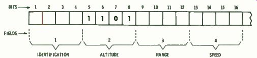
Fig. 9-9. Possible organization of a digital word for an aircraft monitoring
system.
Memory storage elements are flip-flops; Gates 17 and 18 store bit 1 of word 1. In the quiescent state, all inputs are high; memory output bits 0-0 are high ; and match signals M are high (except for match signal Mo). With address bit - A -0 high, Gate 14 is low and Gate 19 is low, regardless of the state of Gates 17 and 18. Therefore, output 1Y° for bit 1 is high. The other bits of word 1 are obtained in a similar manner. With the address bits of the other words also high, their " 19" gates will also be low.
Thus, all outputs are high.
To read out word 1, input A0 is brought low. Gate 19 will now have one input high and will follow Gate 17. If Gate 17 is low, Gate 19 will be low and output Uo will be high. If Gate 17 is high, Gate 19 will be high and output 50 will go low. Thus, the output takes up the state of Gate 18 when word 1 is ad dressed. Suppose that words 1 and 2 are addressed simultaneously by bringing both A0 and A1 low. If both " 19" gates stay high, the output will be low. However, if either of the "19" gates goes low, the output will go high. Gate 19 is actually a wired-OR circuit and if any gate goes low, the common tie-point goes low. For the straight Read function, therefore, the memory is addressed one word at a time as with other memories.
A word is written into the memory by applying it to input s Do through 153, and by bringing the bit enables (E0 through E3) , write enable (WE), and the address bit low. With WE = and X.0 = 0, Gate 15 is free to follow Gate 6, and Gate 16 is
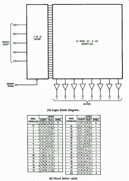
(A) Logic block diagram.
(B) Word Select table.
Fig. 9-8. A 256-bit Read-Only memory.
Fig. 9-10. A 16-bit associative/content addressable memory.
free to follow Gate 7. With É0 = 0, Gates 6 and 7 will follow too or Gate 1. If 150 = 0, Gate 6 goes to a 1; this satisfies Gate 15, which goes to 0. A 0 into Gate 17 drives it to a 1. Gate 18, with two inputs of a 1, goes to a 0. With Do = 0, Gate 1 is 1 and Gate 7 is a 0; thus, Gate 16 remains high. If D0 = 1, Gate 1 goes to a 0, Gate 7 goes to a 1, and Gate 6 to a 0. As a result, Gate 16 is satisfied, which puts a 0 into Gate 18, driving it to a 1, while Gate 17 is driven to a 0. Searching the memory for a match is accomplished by applying the four bits to be matched at inputs 150 through Do and then bringing the E inputs low. First, let all E inputs be high.
Then Gates 20 and 21 of each bit in the memory will have one input low, and none of the "20" and "21" gates will be satisfied.
As a result of this, Gate 24 will be driven high. The group of gates driving Gate 24 are connected in a wired-AND configuration. If any gate is high, it brings the common tie-point high, and Gate 24 is driven low.
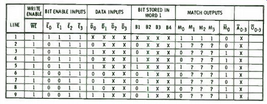
Fig. 9-11. Truth table for Fig. 9.10.
Circuit operation is indicated by the truth table ( Fig. 9-11) . In line 1, all the enable inputs are high and a match is indicated for all words in the memory. For this condition, the state of the D inputs is irrelevant and, thus, the inputs are said to be "masked." In line 2, E0 is brought to a 0, which unmasks bit D0.
The bits stored in the memory for word 1 will affect output 00. If the data bit D0 is a 0 and the bit in storage is 0, output M0 is driven high since bit 0 matches while bits 1, 2, and 3 are masked. If bit 1 of word 2 is also a 0, M1 goes to a 1, but if it is 1, M1 is a 0. Similarly action occurs for words 3 and 4. Lines 3, 4, and 5 show circuit status for D0 and bit 1 of word 1.
In line 6, data inputs 150 and D1 are both unmasked by setting E0 = = 0. No match is obtained in lines 6, 8 and 9, but it is in line 7. The other M outputs will be either high or low depending on the data stored in bits 1 and 2 for words 2, 3, and 4.
The same considerations apply as the other data inputs are unmasked. If the data in all four words is the same as the input or "descriptor" data, then four "match" signals are obtained.
A priority circuit can be used to process the matching words one at a time.
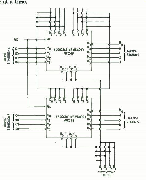
Fig. 9 - 12. Diagram for expanding word length.
A content addressable memory ( or CAM) of larger size can be formed by connecting a number of the basic devices together. As shown by Fig. 9-12, a CAM of 8 words-by-4 bits can be formed from two memory units. The outputs are open collector circuits and, thus, can be tied together. If a match is
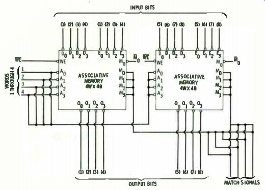
Fig. 9-13. Diagram for expanding bit length.
obtained for the bits being compared, the outputs will be the wired-OR function. The memory can be expanded to more words, in the same manner, by tying together the D inputs, the E inputs, and the 0 outputs.
Expansion to handle 8-bit words can be accomplished as indicated in Fig. 9-13. Match outputs are also open-collector circuits and can be tied together, giving four match signals for a 4-word, 8-bit memory. Expansion to more words and more bits can be obtained by combining the schemes shown in Figs. 9-12 and 9-13.
Prev: PARITY AND PRIORITY
Next: SPECIAL CIRCUITS
Guide Index : Transistor-Transistor Logic (early 1970s)