Standard TTL is presently being used in many digital systems. It has been a popular form of logic for some time. however, as circuit designers became familiar with the characteristics of the family, they began to push against the normal operating limits. At the same time, TTL began advancing from single-gate packages to multiple-gate packages and then to complete functions, such as flip-flops, counters, decoders, etc.
First of all, designers wanted higher speed so they could do certain jobs faster, especially repetitive or time-consuming jobs. Other designers were building computers for use in outer space or in remote locations on earth. They wanted low-power operation so they could run the systems for a long time on batteries. And, of course, all designers would be delighted to obtain both lower power and higher speed at the same time.
In the search for an optimum density of component pack aging, the first stage has become known as small-scale integration ( SSI). Further steps in circuit integration have produced medium-scale integration ( MSI) and large-scale integration (LSI). No hard and fast boundaries separate SSI, MSI, and LSI. Generally accepted definitions are that packages or chips with up to 10 or 12 gates represent SSI; packages containing 10 to 100 gates are MSI; packages with more than 100 gates are LSI. Beyond LSI is something that has been called very large-scale integration ( VLSI). A VLSI device would have 1000 or more gates.
PROPAGATION TIME
What is meant by operating speed in digital systems? A typical gate in standard TTL has an average propagation de lay of about 10 nanoseconds. This means that once the specified input conditions have been met, the output will change to the new state within about 10 ns. For a 2-input NAND gate, the delay in going to a 0 output (from a 1 output) is specified as 7 ns (typical) to 15 ns (maximum) ; the delay in going to a 1 output (from a 0 output) is specified as 11 ns (typical) to 22 ns (maximum). Measuring such delays is difficult and re quires accurate test fixtures, correct operating procedures, and precise definitions of waveshape rise and fall times--when is the output 0 and when is it 1? In practical usage, propagation delay can be translated into the maximum frequency at which a system can operate. A master-slave flip-flop in standard TTL, for example, can be toggled continuously without error as long as the clock frequency is kept below about 30 MHz. (The typical clock frequency is 35 MHz for the type 5470/7470 flip-flop.) At higher frequencies the flip-flop may not respond correctly.
HIGH-SPEED TTL
The first modification to standard type 54/74 TTL was de signed to increase the operating speed. Fig. 11-1 shows the schematic of a basic NAND gate in standard TTL, and Fig. 11-2 shows the schematic for high-speed TTL. High-speed TTL uses lower values of resistance; therefore, the amount of charge storage in these elements and their associated stray capacitances is reduced. Note, also, that high-speed TTL removes the output diode and adds an extra transistor in a Darlington con figuration to aid in changing the output from 0 to 1. As a result of this change, the delay in driving the output to 0 (from a 1) becomes 6.2 ns (typical) to 10 ns (maximum). The delay in driving the output to 1 ( from a 0) becomes 5.9 ns (typical) to 10 ns (maximum). Flip-flops made for high-speed TTL technology can be operated at toggle frequencies of 50 MHz.
One very important parameter-operating voltage-was kept constant at 5-volts dc. Thus, standard and high-speed TTL can be used in the same system without adding special power
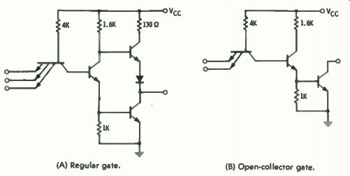
(A) Regular gate. (B) Open-collector gate.
Fig. 11-1. Standard TTL NAND gate.
(A) Regular gate. (B) Open-collector gate.
Fig. 11-2. High-speed TTL NAND gate.
supplies. In all succeeding families of type 54/74 TTL, the operating voltage is kept at 5 volts.
Another notable change incorporated into high-speed TTL (in the type 54/74 family, it is called type 54H/7411) is the addition of clamping diodes on the inputs. Fig. 11-3 shows how these diodes prevent the input lines from overshooting, which, if not suppressed, can lead to false operation. Overshooting and related transient effects become more severe as operating speed increases. The input diodes were found to be so advantageous in type 54H/74H circuits that they have been retrofitted to standard TTL, even though they may not be shown on some drawings. Their inclusion in standard TTL costs practically nothing (other than a change in the masking), and the reduction of coupling problems aids system design.
High-speed TTL has been made available primarily in a number of gating circuits and some assorted flip-flops. Unless the extra speed is actually needed in a circuit, standard TTL is normally used.
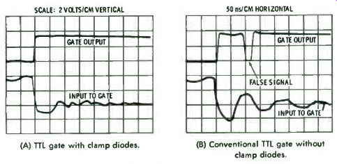
(B) Conventional TTL gate without clamp diodes.
Fig. 11-3. Effect of input clamping diodes.
One of the major prices paid for high-speed TTL is higher power consumption by each gate. In normal operation, standard TTL has an average standby power dissipation of 10 mW per gate. On the other hand, high-speed TTL has a standby power dissipation of 22 mW per gate-more than twice as much. Not only does the higher power requirement place more of a burden on the power supply, it also means that each IC package will give off more heat (assuming an equal number of gates in each package) . Thus, the cooling system requires extra attention, and special fans or heat sinks may be needed.
Because type 54H/74H TTL has lower impedances than standard 54/74 TTL, it uses more input and more output current.
Gates in type 54H/74H circuits can usually drive or fan out to 9 other H gates. Also, one H gate can drive 20 standard gates.
Gates in standard type 54/74 circuits can also drive H gates, but the fan-out from standard to H gates is 1, rather than the usual 10.
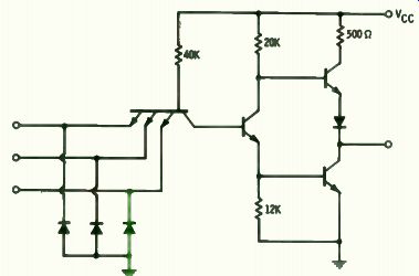
Fig. 11-4. Low- power TTL NAND gate.
LOW-POWER TTL
Since lower circuit impedances in H-type TTL caused power consumption to go up, wouldn't higher circuit impedances cause the power consumption to go down? The answer is yes, and low- power TTL or LPTTL (type 54L/74L) is the result of this idea. The circuit for a basic gate is shown in Fig. 11-4.
Again, the operating voltage is kept at 5 volts.
LPTTL has characteristics similar to standard and high speed TTL, but it pays for its low power consumption in opera ting speed. Power consumption is down to 1 mW per gate, but propagation delay is up to 33 ns per gate. As a result, the flip flop toggle frequency is 3 MHz ( typical) .
ACTIVE BYPASS TTL
The next modification to come along was the use of an active network in the base drive of the bottom output transistor ( Fig. 11-5A) . The effect of the network is shown in Fig. 11-5B. During an output transition from 1 to 0 or from 0 to 1, the output voltage in standard TTL (also high-speed and low-power TTL) will move along the lower curve as shown. With the active by pass network instead of a simple resistor, the upper curve is traced. This means the actual transition periods from low to high and from high to low are decreased, and the result is a slight increase in speed.
The active bypass, as it is called, is used by Motorola in its MC3100/3000 series of devices (also called MTTL III). The impedances used in the basic gate are very close to those in high-speed gates (type H). Power consumption is rated the same for both--22 mW per gate--except that the improved transfer characteristic results in less current-spiking during transitions and, thus, the overall power consumption is lower.
Gate delay is improved slightly over the H-type gate.
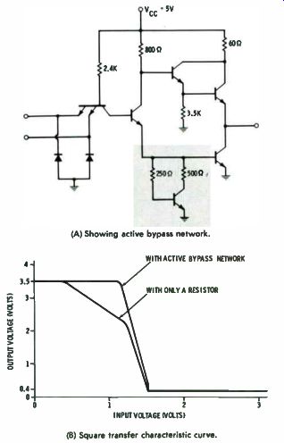
(A) Showing active bypass network.
WITH ACTIVE BYPASS NETWORK OUTPUT VOLTAGE (VOLTS)
INPUT VOLTAGE (VOLTS) WITH ONLY A RESISTOR
(B) Square transfer characteristic curve.
Fig. 11-5. Typical Motorola MTTL III circuit.
SCHOTTKY-CLAMPED TTL
Until the development of Schottky-clamped TTL, all TTL families operated on the principle of saturated logic. That is, transistors were generally overdriven so that their impedance ...
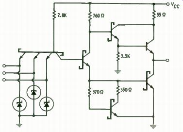
Fig. 11-7. Schottky-clamped TTI gate
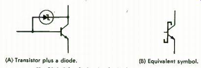
Fig. 11-6. Schottky-barrier diode-clamped transistor. (A) Transistor plus a diode.
(B) Equivalent symbol.
... was as low as possible when they were on and as high as possible when they were off. Because of being overdriven, the circuits required a little extra time to change from one state to the other. A major advantage of this type operation is that it keeps the noise margin high. If the drive is reduced, so that a transistor is turned on but not thoroughly saturated, the noise immunity is also reduced.
Schottky-clamped TTL uses a recently developed component called a Schottky-barrier diode to keep transistors in TTL from saturating. The basic circuit device is an ordinary transistor with a Schottky-barrier diode connected from base to collector as shown in Fig. 11-6A. When base drive is applied to this circuit, the transistor is driven almost into saturation.
At this point, the diode, which has a lower forward voltage drop than the base-collector junction of the npn transistor, takes over and diverts excess current away from the junction.
The diode itself has practically no storage capacity. When base drive is removed, the transistor can follow immediately with out first having to dissipate a stored charge. Thus, the switching characteristic of the combination is significantly better than it is when just a transistor is driven into saturation. The symbol in Fig. 11-6B is used to represent the combination of diode and transistor.
Fig. 11-7 shows a Schottky-clamped TTL gate. In addition to clamped transistors, the circuit uses a Darlington-connected output circuit for the upper part of the totem pole output and the active bypass network for the lower part. The input clamping diodes are also Schottky-barrier type to reduce storage effects. Thus, every change that anybody has been able to think of has been thrown in to increase speed.
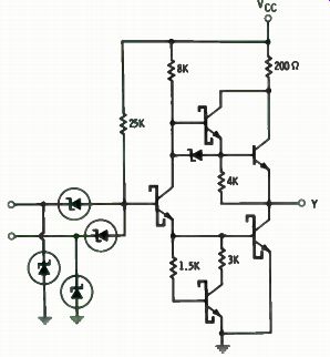
Fig. 11-8. Low-power Schottky in gate with totem pole output.
The result is a basic gate with a propagation delay of 3 ns.
Power consumption is slightly less than the 22 mW-per-gate of high-speed TTL, but the speed is much higher. The family is called type 54S/74S circuits. Flip-flops of this family toggle reliably at 100 MHz.
LOW-POWER SCHOTTKY TTL
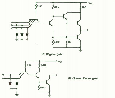
Because Schottky-clamped TTL is so fast, it becomes possible to trade off some of its speed and obtain a savings in power consumption. The result is low-power Schottky TTL, which has only 2-mW dissipation per gate and a propagation delay of 10 ns. The basic circuit for low-power Schottky TTL (or type 54LS/74LS) is shown in Fig. 11-8 for totem pole output and in Fig. 11-9 for open-collector output.
Low power is obtained by raising the impedances of the circuit elements. The input resistor has been increased to 25K from its nominal 1.6K in a standard TTL gate. Note also that the multiemitter input transistor (a common characteristic of TTL) has been replaced by Schottky-barrier diodes. Since ...
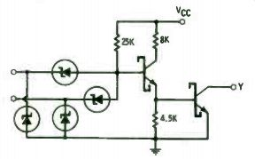
Fig. 11-9.
Low-power Schottky M. gate with open- collector output.
... the diodes have so little storage, little speed, if any, is lost by this change. The input circuit, however, is similar to the input circuit for Diode Transistor Logic (DTL).
TRI- STATE LOGIC
One of the characteristics of TTL is that the output is either high or grounded. Thus, the outputs cannot be connected together, except in the open-collector configuration. But in a data transmission system, in which a single pair of wires is used to carry data back and forth between many different stations, some way of allowing many gates to feed the same circuit is needed. To solve this problem, National Semiconductor Corporation developed what is called Tri-State Logic.
Tri-State Logic, shown in Fig. 11-10, uses extra transistors to control the output circuit. Whenever the control transistor is turned on, it turns both output transistors off. As a result, the output of a Tri-State gate has three states: low voltage, or 0; high voltage, or 1; and high impedance, or OFF. In the first two states, 0 and 1, the gate can feed data into the common line.
In the third state, one of the other gates on the line can feed data into the line. The turned-off gate will not be affected.
Thus, Tri-State Logic allows multistation operation, as long as two outputs are not allowed to talk at the same time. The Tri-State mode of operation has been applied to certain types of gates and devices in all TTL families.
TTL TRENDS
TTL circuits being produced today are primarily in the SSI and MS! class. A great many new functions, especially in MSI, are likely to appear in the next few years. The natural evolution of TTL would seem to be toward complete systems on a single chip, with everything-all the electronics-in one tiny ...
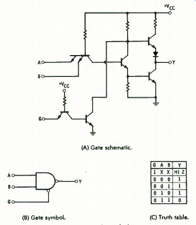
(A) Gate schematic. (B) Gate symbol. (C) Truth table.
Fig. 11.10. Tri-State logic gate.
... package. But a number of factors are working at cross purposes to this development, including power consumption, pack age limitations, and alternative technologies.
When you put 100 standard TTL gates in one package, you have a device with an average power consumption of 1000 mW (1 watt). But, the semiconductor chip itself is only a small part of a small package, and the local heating can be severe.
One limit to the number of gates that can be integrated on one chip is determined by how much power they dissipate and how fast this power-heat-can be conducted away and dumped to the outside world. If the heat is not removed fast enough, the temperature can rise high enough to impair circuit operation and destroy the chip. Cooling effectiveness can be increased by using heat sinks, fans, and even liquid cooling.
Heat generation, on the other hand, can be reduced by using LPTTL circuit concepts of higher impedances and by simplifying internal circuits as much as possible. However, reducing power consumption usually slows things down, which is acceptable in some applications but not in others. To summarize, the power consumption problem may limit the use of TTL to MSI complexity only and may keep it from going very far into LSI. That still, of course, leaves a tremendous field of application.
A second limitation relates to the number of connections the chip can make to the outside world. Two factors are at work here. First, a connection to the outside world requires that a relatively large pad must be metallized on the chip so that a wire can be bonded to the circuit. Space on the chip is at a premium. If you install too many connection pads, you won't have any room left to install transistors and resistors. The second factor relates to the number of pins that can be brought out of a given size package. The more complex a chip is, the more external connections it is likely to require. Dual-in-line packages (called DIP packages), with pins designed to plug into a socket, are available with 14 pins, 16 pins, and so on, up to about 42 pins. As you increase the number of pins, you increase the difficulty of inserting and removing the package from a socket, and you increase the danger of breaking a pin off. You also decrease the reliability of the system because of the increased possibility of a poor connection between the pins and the socket connections.
If a system has only a few inputs and outputs, it can be very complex internally and still fit into a package with a limited number of pins. If the system has many inputs and outputs, the requirement for many interface connections may dictate the use of less complex chips than would normally be used.
The future of TTL will also be influenced by the development of alternative technologies. The most important alternative is Metal-Oxide Semiconductors ( MOS) . A large variety of MOS devices have already been developed, and more are on the way. The major advantages of MOS are its low power consumption and the fact that many more transistors can be placed on a chip than in TTL technology. If LSI and VLSI devices are to
----------------
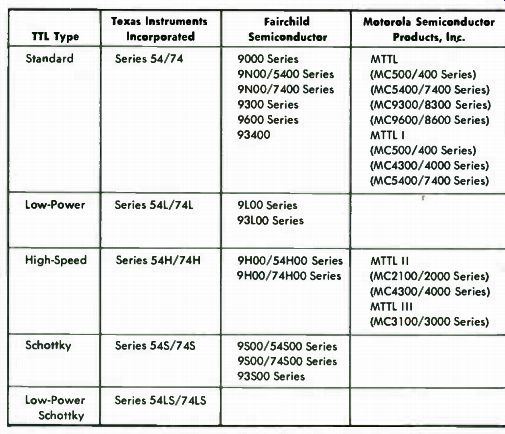
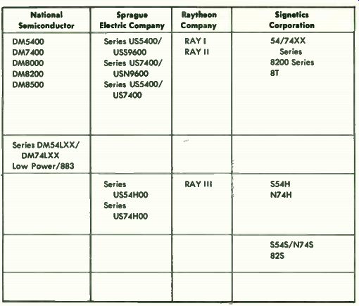

Table 11-1. Major
TTL Type Texas Instruments Incorporated Fairchild Semiconductor Motorola Semiconductor Products, In.
Standard Series 54/74 9000 Series 9N00/5400 Series 9N00/7400
Series 9300
Series 9600
Series 93400 MTTL (MC500/400 Series)
(MC5400/7400 Series)
(MC9300/8300 Series)
(MC9600/8600 Series)
MTTL I (MC500/400 Series)
(MC4300/4000 Series)
(MC5400/7400 Series)
Low-Power Series 54L/74L 9100 Series 93100 Series
High-Speed Series 54H/74H 9H00/54H00 Series
9H00/74H00
Series MTTL II (MC2100/2000 Series)
(MC4300/4000 Series)
MTTL III (MC3100/3000 Series)
Schottky Series 54S/74S 9500/54S00
Series 9500/74S00
Series 93500
Series Low-Power Schottky
Series 54LS/74LS
------------------------
... become popular, it may be that only MOS will be used in these areas. The package problem with respect to the number of pins remains, however. Thus, circuit configurations, such as regular arrays of memory cells, that minimize the problem are favored.
Early types of MOS were much slower than TTL, and they could not compete effectively where speed was important.
Recently developed MOS families are as fast as certain types of TTL. Therefore, much greater use of MOS can be expected.
ECL families, mentioned previously, are still the fastest form of digital logic, and they are being used where the ultimate in speed is necessary. Speed is especially important in large systems where data should be handled as rapidly as possible to obtain maximum use of all circuits. Circuits that have been paid for, but which are seldom used because of a transportation bottleneck somewhere in the system, are very expensive. A circuit that can do a job in 100 ns is obviously working far below maximum efficiency when it is only used once an hour. When there are 10,000 such circuits in a system, the need for data handling speed becomes apparent.
-------------
TTL Families National Semiconductor Sprague Electric Company Raytheon Company Signetics Corporation
System designers look first for a technology that will be able to perform the desired task properly and reliably. If two suitable technologies are found, then the designer will normally choose the least expensive way, if everything else is equal. In real life, of course, "everything else" is never exactly equal.
One method will be more reliable than the other, or weigh less, or be more easily maintained, etc. Economy, nevertheless, is a vitally important consideration. TTL today is a very economical technology. For this reason alone, TTL will continue to see wide and growing use. Added to this is the availability of a great and growing variety of complex circuits and the in creasing familiarity of designers with TTL systems. All these factors mean that TTL will be used in more and more systems.
FAMILIES OF TTL
This guide has dealt primarily with the type 54/74 family of TTL, because this family is the largest and best known. It is manufactured by most of the leading semiconductor manufacturers. Quite a few other TTL families have been developed, of course, since each manufacturer would like to have his own special family.
All TTL families have characteristics similar to type 54/ 74. Sometimes, devices in one or more of the other families can be interchanged directly with type 54/74 devices. In other cases, the devices may perform exactly the same function, but the pin arrangements are different. In addition, some functions are not available in type 54/74 but are available in one or more of the other families. The total number of TTL devices in all families is very large and is growing all the time; thus, a complete listing is not possible here. However, the major families are listed in Table 11-1. Some of the families have only a few devices, while others have hundreds of different circuits.
Even though the table may not show it, many of the families are available from more than one manufacturer. In addition, a number of overseas manufacturers make TTL devices in still other families, some of which are interchangeable with devices from U.S. manufacturers. U.S. manufacturers publish cross reference guides to their own products, and D.A.T.A. ( 32 Lincoln Avenue, Orange, N.J. 07050) publishes guides containing reference data and cross-references to TTL on a world-wide basis.
Prev: Link | --SPECIAL CIRCUITS
Next: TTL APPLICATION
Guide Index : Transistor-Transistor Logic (early 1970s)