This SECTION discusses only two of the many applications of TTL logic. The basic circuit for the Up/Down Counting system was developed by Fairchild Semiconductor. The basic circuit for the Data Transmission system was developed by Texas Instruments Incorporated.
UP/DOWN COUNTING SYSTEM
Counting up or down (depending on the direction in which a part is moving) is very useful in solving some industrial and scientific problems. Fig. 12-1 shows an up/down counting system that uses a light source and photo transistors as signal inputs. An object moving from photo transistor Q2 to photo transistor Q1 causes the count shown by the display tubes to increase by 1; an object moving in the opposite direction causes the count to decrease by 1.
The only significant restriction on the system is that the objects being counted must be large enough to cover both photo transistors at the same time. Up-count information is derived from the fact that an object entering the detection area, first interrupts the light input to transistor Q2, then to both transistors Q2 and Q1, then to transistor Q1 only, and finally, to neither. Down-count information is derived from the reverse sequence.
When no object is present, transistors Q1 and Q2 are on.
This allows current to flow through resistors R1 and R2 to ground, turning transistors Q3 and Q4 on. Therefore, Gates ...
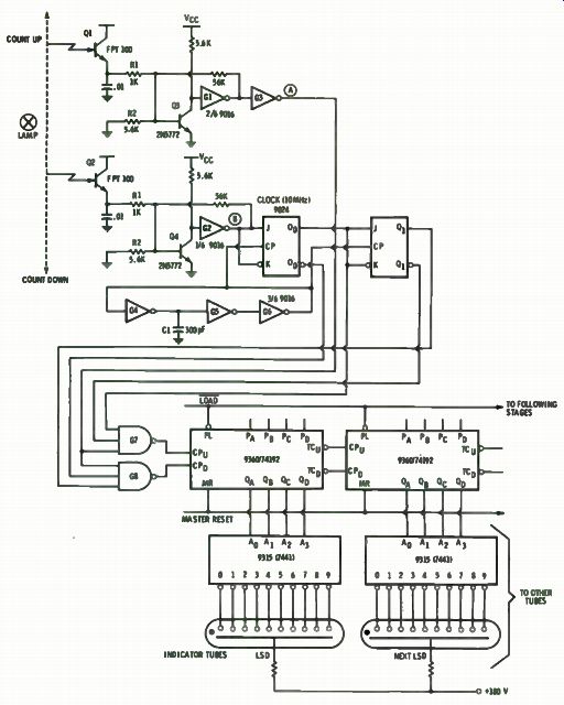
Fig. 12-1. An up/down counting system.
... G1 and G2 have low inputs and high outputs; thus point B is high and point A is low. Point A thus holds the outputs of Gates G7 and G8 high.
Gates G4, G5 and G6, in combination with the capacitor C1, form a free-running clock that operates at about 10 MHz.
When Gate G4 goes low, it discharges the capacitor and drives Gate G5 high and Gate G6 low. When Gate G6 is low, it drives G4 high. But when Gate G4 goes high, it must first charge up capacitor C1 before the voltage at the input of Gate G5 rises sufficiently to switch the gate low. Thus, the circuit operates as a relaxation oscillator to provide clock pulses to the two flip flops.
The flip-flops form a 2-bit shift register. As long as point B is high, the first flip-flop holds a 1 ( Q0 = 1) , which in turn puts a 1 into the second flip-flop. Gates G7 and G8 are held high by Q0 = Q1 = 0. Let an object enter the detection area in the count-up direction. Transistor Q2 is covered first, which removes most of the drive current to transistor Q4 and turns it off. This puts a high at the input of Gate 2 and a low at point B. The next clock pulse, after point B goes low, puts a 0 into the first flip-flop; the next clock pulse puts a 0 into the second flip-flop. At this point, Gates G7 and G8 each have two Os and a 1 as inputs and, there fore, are high.
The object moves further to cover transistor Q1 while transistor Q2 is still covered. This drives point A high. Gates G7 and G8 now have two is and one 0 as inputs.
The object next uncovers transistor Q2, which causes point B to go high, and the next clock pulse puts a 1 into the first flip-flop. At this point, Gate G7 has all is as inputs and goes to 0, while Gate G8 has two is and a 0. The negative transition on the Count-Up input to the counter causes the device to advance one count. On the next clock pulse, Gate G7 is again disabled by transistor Q1 = 0. As the object advances further, it clears transistor Q1, and point A again goes low.
When an object enters from the opposite direction, point A goes high first. As transistor Q2 is covered, point B goes low, which allows a 0 to enter the flip-flop. This condition of 0 in flip-flop 1 and 1 in flip-flop 2 opens Gate G8 for one clock pulse, which causes the counter to make a down count.
Only two decades of counting are shown but more can be added. The system can be modified to generate a signal when a preset count is reached.
DATA TRANSMISSION SYSTEM
One of the major advantages of digital systems is that they can handle information without being degraded by noise. This characteristic allows data to be transmitted long distances through noisy channels without loss of information. However, digital signals are not immune to noise; if sufficient interference occurs, they can be completely lost, just like an analog signal. But, as long as the signal-to-noise ratio is kept above a minimum, the signal can be transmitted without error.
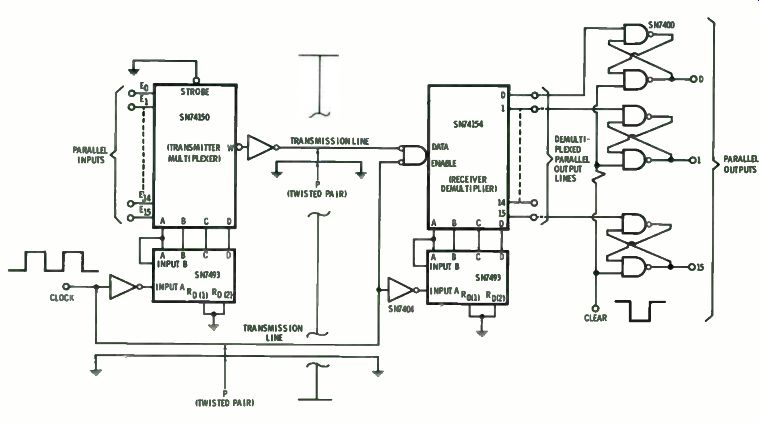
Fig. 12-2. Logic diagram for a digital data transmission system.
Fig. 12-2 shows a straightforward transmission system for digital data. The data is available at the transmitting end of the communications link in the form of 16-bit, parallel words.
To keep the cost of wiring between transmitter and receiver low, the data is to be sent serially over one pair of twisted wires. To keep the electronic encoding and decoding system uncomplicated, a second pair of twisted wires is used to synchronize the operation of transmitter and receiver. For relatively short transmission links ( as in a factory between a production line and a central computer), the separation of data channel from control channel is practical and economical. In longer links and in more complex systems, control and data can be transmitted over the same pair of wires-or radio channel, etc.
The 16-bit word is applied to the 16-parallel inputs of the data selector/multiplexer, type SN74150 (Fig. 12-2) . With the Strobe input 0 (grounded, as shown), the multiplexer will de liver the input bits to the outputs, one at a time, under control of the address or select inputs A, B, C, and D. The address bits are obtained from a binary counter, circuit type SN7493. The counter is connected to run as a 0 to 16-bit counter. Thus, as it passes through its count sequence, it will generate the required 16 address codes for the SN74150 multiplexer.
The clock signal is obtained from an oscillator. Assuming the clock is a positive-going signal, an inverter is required at the input of the binary counter, since it operates on the negative edge of the clock pulse.
The clock signal is also fed over a second pair of transmission lines to an identical inverter at the input to a 16-bit binary counter at the receiver. The data coming out of the multiplexer appears in inverted form; therefore, an inverter is used to restore the data to its true form. It is then sent over the line to the receiver.
At the receiver, a 4-line-to-16-line decoder/demultiplexer (circuit type SN74154) acts to sort out the stream of serial bits and reconstruct the original transmitted word. When Data and Enable inputs are both low ( Fig. 12-3), the SN74154 de multiplexer causes the addressed output to go low. Thus, when the address is 0000, output 0 is addressed. It will follow the Data input, going low if Data is low; otherwise, output 0 stays high.
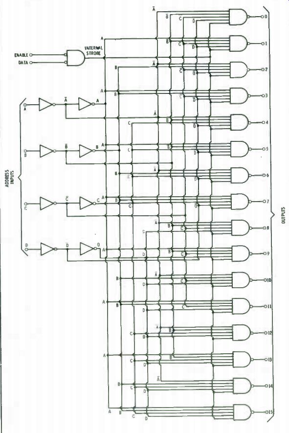
Fig. 12-3. Decoder/demultiplexer logic diagram (type SN74154).
Assume first that the two addressing circuits start out from 0000 together and stay in step throughout the operation of the system. This can be assured by resetting the counters to 0000 before every transmission. With the counters in step, both the multiplexer and the demultiplexer will always be addressing the same bit. The time delay over the transmission path is assumed to be close to zero and, therefore, negligible. The sequence of operation can be deduced from the waveforms of Fig. 12-5. As each bit ( E0 through E,,) of the word to be trans mitted is addressed, it appears at the input of the demultiplexer. When the clock goes low, the bit appears at the output of the demultiplexer. Note that, if the bit is a 1, no change occurs in the output of the demultiplexer, since its normal or quiescent output is a 1. If the bit is a 0, the addressed output goes low, and all other bits are high.
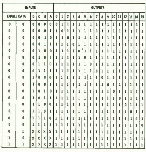
Fig. 12-4. Truth table for Fig. 12-3.
If the received data can be used in this format, no further processing is required. But if the word is to be "captured," each individual bit must be stored until the complete word is received. This can be accomplished with the latch circuits ( Fig. 12-2). Before a word is transmitted, the latches are all set to 1 by driving the Clear line to 0. Then, as the word is received, any bit that is a 1 does not affect its associated latch, but any bit that is a 0 drives its latch to 0. Thus, the word is captured.
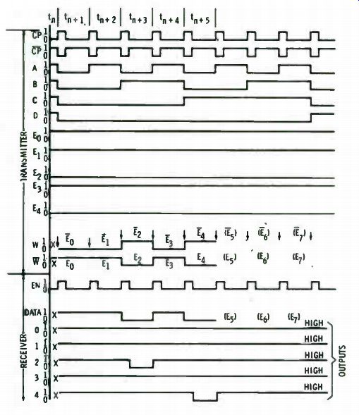
Fig. 12-5. Waveforms for Fig. 12-3.
The data transmission system described above can be modified and elaborated in many ways. Two-way transmission may be necessary; multistation operation with point-to-point dial up may be needed, etc. Digital techniques can be applied in each case. If the transmission lines are too noisy, line drivers and receivers can be used to reduce errors.
Prev: INCREASING TTL SPEED AND DEVICE DENSITY
Next: DIGITAL LOGIC CONVENTIONS
Guide Index : Transistor-Transistor Logic (early 1970s)