The basic symbols used in digital electronics are relatively few in number, but they must be interpreted rigidly. A gate may perform one function for positive logic and a different, but equally valid, function for negative logic. So watch out.
For the symbols shown, let a 1 be a positive voltage of about 3.5 volts, and let a 0 be zero volts. In positive logic, a signal is called "True" when it is a 1 and "False" when it is a 0. We are primarily interested in true statements, not false statements, because a true statement means that a certain set of specified conditions have been met. A false statement means only that the conditions have not been met, which is often useful but is not very precise.
The AND function is shown by the open D symbol ( Fig. A 1A). When inputs A AND B are true-that is, 1-then the output is true, or a 1. If either input A or input B is not 1, then output Q is 0, or false, which means the AND function has not been satisfied. But output Q being a 0 does not tell us whether A or B is a 0 or if both are 0. The truth table lists all possible combinations of inputs and the resulting output for each condition. Only two inputs are shown, but the same logic applies for more inputs: all must be a 1 for output Q to be a 1.
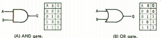
(A) AND gate. (B) OR gate.
Fig. A-1. Basic logic gates and their truth tables.
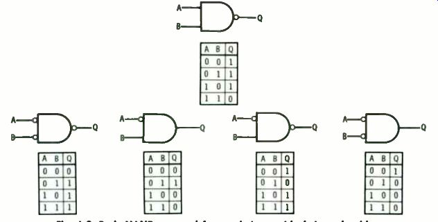
Fig. A-2. Basic NAND gate and four variations, with their truth tables.
The symbol for an OR gate is similar to that for an AND gate, except the input line is curved ( Fig. A-1B). Again, the truth table spells out all the states of the circuit.
The NAND symbol is an AND gate with an open circle on the output to indicate negation. Output Q is a 0 when inputs A and B are both high. Fig. A-2 shows a basic gate and four variations.
A NOR gate is a negated or inverted OR gate. The symbol has an open circle on its output. The basic gate and four variations are shown in Fig. A-3.
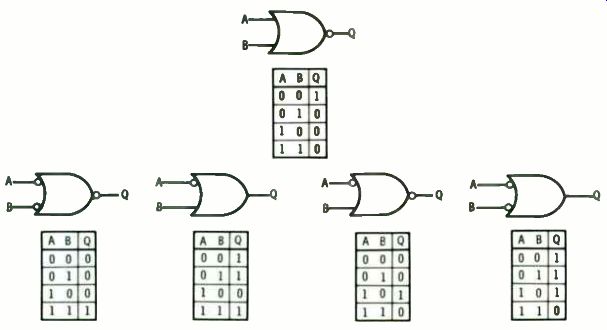
Fig. A-3. Basic NOR gate and four variations, with their truth tables.
(A) Amplifier gate. (B) Inverter gate. (C) Exclusive-OR gate. (D) Exclusive-NOR gate. (E) Wired-OR connection.
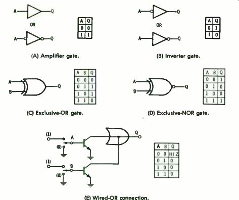
Fig. A-4. Other logic gates and their truth tables.
Sometimes gates have inverters on one or more inputs and/ or outputs. The effect of these inverters is to make a 0 a true input or to show that the output goes low when the gate is satisfied. Fig. A-4 shows the symbols and truth tables for amplifiers ( a triangle), inverters (triangle with open circle on input or output), an exclusive-OR gate, an exclusive-NOR gate, and a wired-OR configuration.
Prev: TTL APPLICATION
Next: NUMBERING SYSTEMS
Guide Index : Transistor-Transistor Logic (early 1970s)