Machine-to-machine communications are accomplished primarily with binary numbers ( radix 2), and, since man is most at ease with decimal or radix ten numbers, the need to trans late information from one number system to the other occurs constantly. The task of converting a radix ten number (any number from 0 through 9) to a radix 2 number (0 or 1) is usually called encoding; going from radix 2 to radix 10 is usually called decoding.
Encoding devices are usually found at the input terminals of digital systems. They usually are not complicated in their logical structure. To encode a number 9, for example, we only need to set four toggle switches to either a high voltage or ground, in such an order that they permit an output corresponding to the code 1001. Decoding, on the other hand, re quires the logical analysis of a number of inputs to determine which output is correct.
Digital circuits are constantly required to decode a set of input signals and generate a specific output. If a circuit is driving a set of signal lights, then each light must have its own specific address. If a circuit is driving a seven-segment read out device, the circuit must be able to choose which segments to light and which to leave dark. If a circuit is operating with a magnetic core memory, some means must be provided to address each specific word location in the memory, both for reading in and reading out. This SECTION will discuss some TTL decoders.
ONE-OF-FOUR DECODER
One of the simplest TTL decoders is the Fairchild TTL/MSI 9321, a " Dual One-of-Four Decoder." The functional block dia gram is shown in Fig. 3-1A. (The TTL/MSI 9321 is a member of a TTL family very similar to and compatible with type 54/74 circuits. A similar decoder, but a little more complicated, is circuit type SN54155/SN74155.) The circuit has two data inputs, Ao and A1 , and an enable input E. The enable input is a
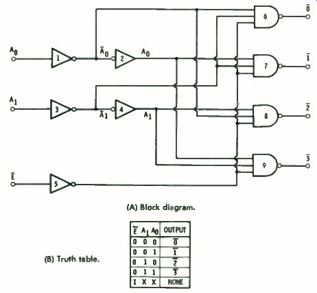
(A) Block diagram. (B) Truth table.
Fig. 3-1. Dual one-of-four decoder.
control input and allows the circuit to be synchronized by a clock signal. Inputs Ao and A1 are the inputs to be decoded, and together they form the digital word A1 Ao, as shown in the truth table in Fig. 3-1B. The word A1 Ao can be any one of four combinations, and the decoding circuit must determine which of the four outputs to choose for each input word. The outputs are labeled: 15, i, 2, and U. The selected output goes to 0 while the others stay high.
The circuit can be considered to consist of four major sections as shown in Fig. 3-2--input address, control, logic, and
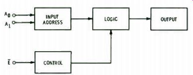
Fig. 3-2. Basic functions of a decoder circuit.
output. When convenient, these various sections in other ICs are allowed to merge into one another and thus cannot always be clearly identified. In the 9321, Gates 1 through 4 ( Fig. 3-1A) form the address section, Gate 5 forms the control, and Gates 6 through 8 form the logic. The output section in this device is simply the outputs of Gates 6 through 8, each of which goes to a separate pin of the IC package and can drive a specific load.
In the input section, Ao drives Gate 1, an inverter. Gate 1 drives Gates 2, 6, and 8. Without Gate 1, any circuit trying to drive input Ao would have to supply three input circuits; with Gate 1, the device presents an ordinary unit load to the driving circuit.
Gate 1 is followed by Gate 2, which is another inverter. Gate 1 gave buffering and ro; Gate 2 gives back Ao. Both Ao and Ao are needed to drive the logic section.
The control section consists only of an inverter. Note that when the enable signal = 1, the output of Gate 5 is 0, and the outputs of Gates 6 through 9 are all 1s; this is the quiescent state of the decoder. When E = 0, then Gate 5 = 1, and Gates 6 through 9 are controlled by Ao and Al. The state of the circuit for E = 1 is given by line 1 of the analysis table in Fig. 3-3-all outputs are high.
Lines 2 through 5 show the status of the circuit for the four combinations of A1 Ao. With Ao = A1 = 0 and E = 0 (line 2),
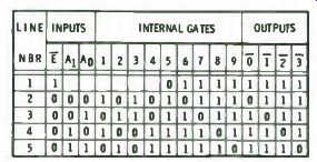
Fig. 3-3. Analysis table for Fig. 3-1.
Gate 6 has a 1 on each input, and thus has an output of 0; output 15 is low. Gate 8 has one input low ( A1 through inverter Gates 3 and 4) and is therefore high; Gate 9 has two inputs low (the outputs of Gates 2 and 4) and is high. Gate 7 is driven high by the input from Gate 2. Thus, all output gates except 6 are high.
Line 3 shows the condition of the gates for Ao = 1 and A1 = 0. The logic function of the device causes all output gates to go high except Gate 7, thereby selecting - 17 as the output line.
The other two input code combinations ( shown on lines 4 and 5) operate similarly to select output - 2 . or output U.
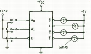
Fig. 3-4. Typical decoder circuit configuration.
Fig. 3-4 shows how the device can be used to light any one of four lamps, depending on the input word A1 Ao and control E. When an output is low, current will flow from +5-volt source through the lamp to ground causing the lamp to light.
Again, open circles on the block symbol indicate that a low signal is required for circuit operation ( or that the selected output goes low).
ONE-OUT-OF-TEN DECODER
Three different ICs have been developed in the type 54/74 family to decode three different number codes. These are known as the Binary-Coded-Decimal code ( BCD), the Excess-3 code, and the Excess-3 Gray code. The three devices are very similar in logical structure and use the same decoding concept as the previously discussed one-out-of-four decoder.
The functional block diagrams for the decoders are shown in Figs. 3-5, 3-6, and 3-7. The decoders do not have an enabling input. Their truth tables are shown in Fig. 3-8.
Decimal numbers from 0 through 15 are shown at the left of the truth tables. Truth table A shows the BCD code for the decimal numbers. The binary number 0000 represents decimal number 0; binary number 0001 represents decimal number 1; binary number 0010 represents decimal 2; etc.
Truth table B shows the Excess-3 binary code, where binary number 0011 represents decimal 0, binary 0100 represents decimal 1, etc. The Excess-3 code is obtained by giving decimal 0 the binary number 0011, which is the same as decimal 3 in BCD. Thus, in Excess-3, the count starts at the equivalent of decimal 3 and ends at decimal 12.
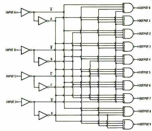
Fig. 3-5. Functional block diagram for a BCD-to-decimal decoder.
Truth table C shows Excess-3 Gray binary code, where bi nary number 0010 represents decimal 0, etc. The Gray code was originally set up so that no more than 1 bit would change, when counting in sequence from one number to the next higher or lower number. Truth table C shows the Excess-3 version of the Gray code.
Assume you are decoding a BCD signal, and the binary word 0000 is presented to the decoder. The gate controlling output 0 will have as inputs À, II, e, and ti, which are all is, and the ...
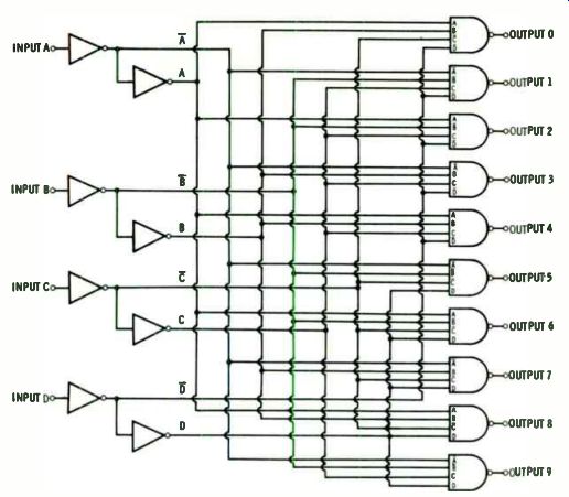
Fig. 3-6. Excess-3-to-decimal decoder functional block diagram.
... gate will go to 0. This is shown by the output truth table D in Fig. 3-8. Examination of the logic diagram will show that all the other output gates have at least one input at 0, and thus they will be high. If the input code changes to 0(101, the 1 output goes low and the others all go high.
If the signal to be decoded is in Excess-3, we use circuit type 5443/7443, shown in Fig. 3-6. For an input of 0011, the logic again drives output 0 low and all the other outputs high.
Circuit type 5444/7444 decodes Excess-3-Gray signals.
In all three ICs, four inputs are required. Note that with four inputs, there are 16 possible input combinations. Since only 10 outputs are needed, six of the input combinations are meaningless so far as selecting an output is concerned, and so all outputs are high for these inputs. ( Remember from Fig. 3-4 that a low output is necessary for circuit operation.) The three ICs do not have a control section, and thus clocking or enabling is not possible or required. The outputs tend to follow the inputs instantaneously, subject only to the propagation delays of each block in a given chain or path. The shortest ...
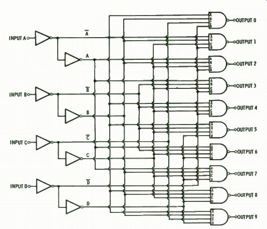
Fig. 3-7. Excess-3-Gray-to-decimal decoder functional block diagram.
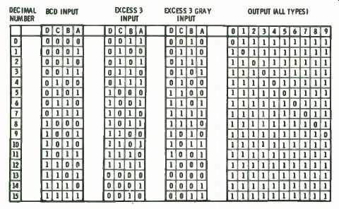
Fig. 3-8. Truth tables for Figs. 3-5, 3-6, and 3-7.
... signal path is through two blocks consisting of an input inverter and the output NAND gate; the longest path is through two inverters and the output gate.
Many times, a 1-of-10 decoder will be required to decode signals for driving a Nixie tube. Since Nixie tubes require about 170 to 180 volts for operation, the typical TTL IC can not be directly connected but has to drive buffer transistors having adequate voltage ratings. In the type 7441 BCD-to-deci mal decoder/driver shown in Fig. 3-9, the buffer transistors are built in, and the IC can drive a Nixie tube direct.
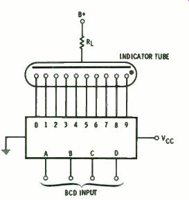
Fig. 3-9. Block symbol for a BCD decoder with direct- drive capability.
Several other decoding ICs have built-in buffer transistors for driving relatively heavy loads. Circuit type 5445/7445 has buffer output transistors rated at 30 volts, and circuit type 54145/74145 has output transistors rated at 15 volts. The output transistors are open-collector type and can sink 80 mA. These devices can drive relays and low-voltage lamps, but not Nixie tubes. The truth table shown in Fig. 3-8A and the functional block diagram ( Fig. 3-5) apply also to these two devices.
SEVEN-SEGMENT DECODERS
Fig. 3-10 shows how an indicator tube consisting of seven individual straight-line elements can be used to form numerals from 0 through 9. To form a 7, for example, we light sections a, b, and c and leave the others dark.
When using 7-segment tubes as display elements, special de coders are needed to interpret the input signals and to light up
the correct segments of the display tube. The problem is similar to choosing one input out of ten possible inputs, except that now multiple outputs are needed for each input code-from 2 outputs for numeral 1 to 7 outputs for numeral 8.
Several types of ICs have been developed for decoding in puts and driving 7-segment indicators. The basic decoding logic block diagram is shown in Fig. 3-11. The truth table is shown in Fig. 3-12. The control section of the circuit consists of the Blanking Input ( BI). When BI = 1, Gate 1 is also a 1.
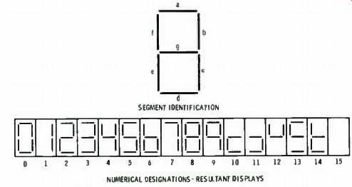
Fig. 3-10. Seven-segment indicator tube.
The NAND gates driven by Gate 1 are responsive to inputs A, B, C, and D, and act as the inverters did in previously discussed de coders. To obtain output numeral 1, we need to light segments b and c ( Fig. 3-10). The truth table shows that the inputs must be A = 1 and B = C = D = 0. Looking at the output section, note that each segment is controlled by an AND gate but operates with inverted inputs.
Fig. 3-13 shows the logic symbol and truth table for a two input AND gate of this type; for a true output ( 1) from this gate, all inputs must be low ( 0) . For segment a, in Fig. 3-11, one input to the output gate is B and D; this output is obtained from an AND gate, and since B = D = 0, this signal is a 0. The next input to the a-segment gate is A • C. Since A = 1, À = 0 and C = 0, this input to the output gate = 0. The last input is A • É • C • D. Since A = 1 and = e = D = 1, the output of the AND gate is 1 and, thus, the third input to the a-segment output gate is high; the output signal is 0. In this IC, a selected output must go high; thus, segment a is rejected.
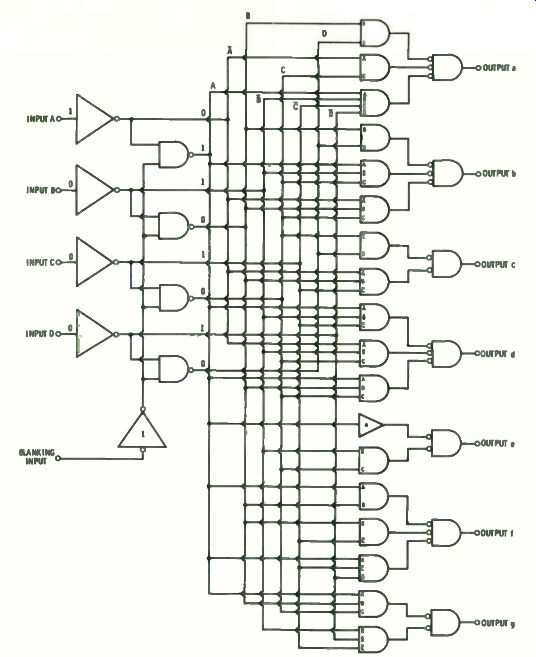
Fig. 3-11. Block diagram for typical IC used to drive indicator tubes.
Similar analysis for segment b shows that the three inputs to its output gate are:
B•D=0•01=0
A• È•C=0•1•0=-0
À•B•C=0•0•0=0
The b-segment gate is satisfied with three low inputs, and its output is high.
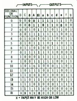
Fig. 3-12. Truth table for Fig. 3-11.
For the c-segment gate, inputs are: C•D=0•0=-0 A•B•"=0•0•1=0
Thus, the output is high.
For the d-segment gate, inputs are:
A • • C = 1 • 1 • 1 = 1
À•È•C=0•1•0=0 A•B•C=1•0•0=0
Since the d-segment gate is not satisfied, its output is low.
Similar analysis for segments e, f, and g will show them to be low for the input code being considered. As the inputs are changed, the segment gates go high or low in accordance with the truth table.
The outputs follow the input code without delay or clocking.
When the blanking input goes low, it causes the gates it drives
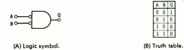
(A) Logic symbol. (B) Truth table.
Fig. 3-13. Two- input AND gate with inverted inputs.
to go low regardless of the input signals. This gives as inputs to the decoding logic the inverted input signals A, B, C, and D, plus the internally generated signals A=B=C=D= 1. Thus, for inputs to the a-segment gate (? = unknown) , we have:
B•D= 1• 1 = 1
• C = ? • 1 = ? A • • • r).1•?•?•?.?
Since the gate has at least one input = 1, its output = 0. Examination of the other output gates shows that all have at least one input high; thus, all outputs are low. Since the segments are energized only when BI = 1, this input can be used to turn the segments on and off on a regular basis. Leaving the indicators off part of the time saves operating power and gives control over the brightness of the resulting display. The on/off cycle should be short-30 cycles per second or so-to prevent the display from flickering.
LAMP TEST AND RIPPLE BLANKING
When circuits have a number of lamps that show output or internal conditions, the possibility always exists that one or more of the lights may become defective-burned out, loose in its socket, etc. A lamp-test provision allows an operator to close one push button or switch causing all lamps, or all lamp segments in a seven-segment display, to turn on, regardless of the state of its normal inputs. Any lamp or segment that fails to turn on, in this test, can be assumed to be defective and require maintenance.
Fig. 3-14 shows the basic 7-segment decoding logic diagram of Fig. 3-11, but with several additions. First, all the outputs have inverters, which generally use relatively high-volt age (30 V or 15 V) transistors to boost the power-handling capability of the IC. Signal inversion produces active low outputs instead of active high; thus, the output section of the truth table is the negative (reverse) of the previous circuit.
Three other inputs must be accounted for. These are ( 1) the "Blanking Input/Ripple-Blanking Output" ; ( 2) "Lamp Test" ; and (3) "Ripple-Blanking Input." The connection BI/RBO uses wired-OR (or wired-AND) logic, which is discussed in SECTION 1.
Consider first the lamp-test input (LT). This signal passes through a negated input inverter which acts as a buffer amplifier. Thus, when LT = 1, it does not affect Gates 1, 2, 3, 4, or 5.
When LT = 0, Gates 1, 2, and 3 are driven high. Also, the wired connection between Gates 4 and 5 requires that when LT = 0, BI/RBO must be open or high. With LT = 0, Gate 5 is driven high, which drives Gate 4 high; with Gates 1, 2, and 3 also driven high by LT = 0, and Gate 4 high, Gates 6, 7, and 8 are driven low. The logic diagram has been marked to show the state of Gates 1 through 10 when LT = 0. Further examination of the logic diagram shows that all the output inverters will have a 1 input except output g, which could be on or off depending on input D. Therefore, the LT signal is brought to the g segment to insure complete testing.

Fig. 3-14. Block diagram of circuitry having provision to test for indicator
lamp failure.
Next, consider the Ripple-Blanking Input. Ripple blanking is used to turn off indicators that are not required in a display.
If you have a six-digit display running from 000000 to 999999, but want to show only the number 387, you can show it as 000387 or you can blank out the three leading zeros. Blanking out the leading and trailing zeros makes the display easier to read.
When RBI = 1, Gate 5 will have a 0 input and will be high.
With Gate 5 high, the decoding circuitry is free to follow inputs A, B, C, and D. All numerals will be decoded and displayed, including ZERO.
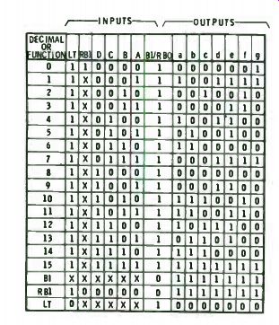
Fig. 3-15. Truth table for Fig. 3-14.
However, when RBI = 0, the output of Gate 5 depends on in puts A, B, e, and D ( LT must be high for normal circuit operation). If inputs A=B=C=D= 0, then = e= 1, and Gate 5 has all is for inputs. Gate 5 is satisfied and goes to 0. With Gate 5 = 0, all segments go high, which is the off condition. Thus, the numeral ZERO is not lighted-it is blanked out. All other numerals from 1 through 9 are displayed normally.
At the same time that ZERO is blanked, the input/output pin BI/RBO is driven to 0. Fig. 3-16 shows how this operating mode can be used for ZERO blanking in a six-numeral display.
In this application, the decimal point location is fixed, and the
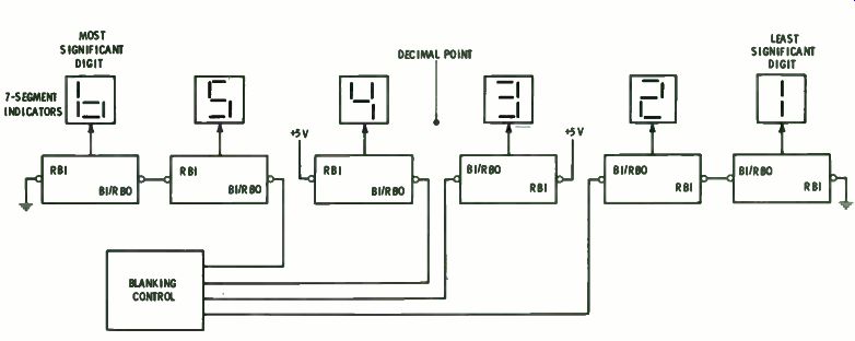
Fig. 3-16. Readout display with Blanking Input/Ripple-Blanking Output capabilities.
decoders on each side of it have their RBI terminals permanently connected to highs. These connections prevent these two digits from blanking out when they are asked to display a ZERO. This type operation helps prevent errors in placing the decimal point when reading the display.
The digits farthest removed from the decimal point have the RBI terminal grounded. This causes the logic to blank out ZEROs in these positions.
The digits in the intermediate positions must respond a little differently. If the Most Significant Digit (extreme left-hand digit) is not a ZERO, then the numeral for the next most significant digit must be lighted, even if it is a ZERO. Considering digit 6, we note from Fig. 3-16 that its RBI terminal is grounded (that is, = 0). Thus, when A=B=C=D=0 for this digit, the ZERO is blanked and its Ripple Blanking Output is driven to 0. Since this signal acts as the RBI for digit 5, digit 5 will react similarly to digit 6. If the BI/RBO signal from digit 6 is 0, digit 5 will also blank out a ZERO (when its input A = B = C = D = 0). If the BI/RBO signal from digit 6 is a 1, digit 5 will display an output, even if it is a ZERO.

Fig. 3-17. Major characteristics for BCD-to-seven-segment decoder/driver.
Digit 1 acts similarly to digit 6; digit 2 acts similarly to digit
5. Digits 3 and 4 always present a display, even when the numeral is ZERO. If the intensity of the display is to be controlled, the blanking input can be modulated with a multivibrator. Best results are obtained using a modulation source that allows the duty cycle to be varied.
Major characteristics of various BCD-to-seven-segment ICs are shown in Fig. 3-17.
Prev: Link | --FLIP-FLOPS
Next: MULTIPLEXERS
Guide Index : Transistor-Transistor Logic (early 1970s)