The following represent rule-of-thumb answers to questions regarding the use of TTL circuits. These should not be adhered to on an absolute basis; rather, they should be treated as guidelines.
------------
------------
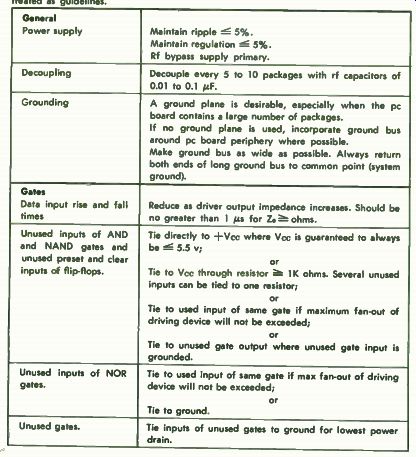
General
Power supply
Decoupling
Grounding
Gates Data input rise and fall times Unused inputs of AND, and NAND gates and unused preset and clear inputs of flip-flops.
Unused inputs of NOR gates Unused .3a - es.
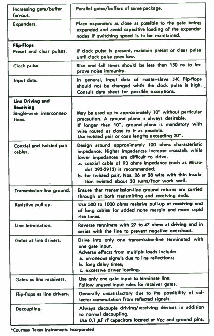
Increasing gate/buffer fan-out.
Expanders.
Flip-Flops Preset and clear pulses.
Clock pulse.
Input data.
Line Driving and Receiving Single-wire interconnections, Coaxial and twisted pair cables.
Transmission-line ground.
Resistive pull-up.
Line termination.
Gates as line drivers.
Gates as line receivers.
Flip-flops as line drivers.
Decoupling.
----------------------
Maintain ripple -- 5%. Maintain regulation -- 5%. Rf bypass supply primary.
Decouple every 5 to 10 packages with rf capacitors of
0.01 to 0.1 µF. A ground plane is desirable, especially when the pc board contains a large number of packages.
If no ground plane is used, incorporate ground bus around pc board periphery where possible.
Make ground bus as wide as possible. Always return both ends of long ground bus to common point (system ground). Reduce as driver output impedance increases. Should be no greater than 1 ms for Z. •-•' ohms.
Tie directly to + Vcc where Vcc is guaranteed to always be ••• 5.5 v; or Tie to Vcc through resistor .•. 1K ohms. Several unused inputs can be tied to one resistor; or Tie to used input of same gate if maximum fan-out of driving device will not be exceeded; or Tie to unused gate output where unused gate input is grounded.
Tie to used input of same gate if max fan-out of driving device will not be exceeded; or Tie to ground.
Tie inputs of unused gates to ground for lowest power drain.
Parallel gates/buffers of same package.
Place expanders as close as possible to the gate being expanded and avoid capacitive loading of the expander nodes if switching speed is to be maintained.
If clock pulse is present, maintain preset or clear pulse until clock pulse goes low.
Rise and fall times should be less than 150 ns to improve noise immunity. In general, input data of master-slave J- K flip-flops should not be changed while the clock pulse is high. , Consult data sheet for possible exceptions.
May be used up to approximately 10" without particular precaution. A ground plane is always desirable.
If longer than 10", ground plane is mandatory with wire routed as close to it as possible.
Use twisted pair or coax lengths exceeding 20". Design around approximately 100 ohms characteristic impedance. Higher impedances increase crosstalk while lower impedances are difficult to drive.
a. coaxial cable of 93 ohms impedance (such as Micro dot 293-3913) is recommended;
b. for twisted pair, Nos. 26 or 28 wire with thin insulation twisted about 30 turns/foot work well.
Ensure that transmission-line ground returns are carried through at both transmitting and receiving ends.
Use 500 to 1000 ohms resistive pull-up at receiving end of long cables for added noise margin and more rapid rise times.
Reverse terminate with 27 to 47 ohms at driving end in series with the line to prevent negative overshoot.
Drive into only one transmission-line terminated with one gate input.
Adverse effects from multiple loads include:
a. erroneous signals due to line reflections;
b. long delay times;
c. excessive driver loading.
Use only one gate input to terminate line.
Follow unused input rules for receiver gates.
Generally unsatisfactory due to the possibility of collector commutation from reflected signals.
Always decouple driving/receiving devices in addition to normal decoupling.
Use 0.1 µF rf capacitors located at Vcc and ground pins.
---------------------
Prev: Link | --TTL POWER SUPPLY
Next: GLOSSARY
Guide Index : Transistor-Transistor Logic (early 1970s)