AMAZON multi-meters discounts AMAZON oscilloscope discounts
This section is devoted to typical digital meter circuits (the integrating digital meter is discussed further in a later section). Several instruments have been selected for discussion. These represent a cross section of digital meter circuits in current use.
LOGIC CIRCUITS AND BINARY COUNTING MACHINES
To fully understand the operation of digital meters it is necessary to understand logic circuits and the various binary counting systems.
Thus, before going into the details of digital meter circuits, these subjects will be summarized in the following paragraphs.
Binary Counting Systems
The binary counting system is used in digital computers, pulse code modulation telemetry, and in various other electronic equipment.
In the binary system each number is made up using only zeros and ones, rather than zero through nine as in the familiar decimal systems.
Consequently, instead of requiring ten different values to represent one digit the various forms of digital equipment using the binary method need only two values for each digit. In digital equipment the values are easily indicated by the presence or absence of a signal, or by positive and negative signals, or perhaps by two different levels.
One of the easiest ways to understand the binary counting system is to compare it with the more familiar decimal system. In the decimal system the value of each digit is based on ten and the powers of ten.
When you read these (decimal) numbers, you automatically add all of the ones, tens, hundreds, thousands, etc. Take the number 3733, for example. You could read this as "three seven three-three," but more than likely you would read it as "three-thousand, seven-hundred and thirty-three." The decimal number 3733 means:

-------------
In other words, you can say that the extreme right-hand digit is multiplied by one, the digit second from the right is multiplied by 10, the digit third from the right is multiplied by 100, and the digit fourth from the right is multiplied by 1000. In the binary counting system the value of each digit is based on two and the powers of two. This can be displayed as follows : 256 128 64 32 16 8 4 2 1
In the binary system, if the digit is a zero, its value is zero. If the digit is one, its value is determined by its position from the right. For example, to represent the number 77 in binary numbers, the following combination of zeros and ones must be used:
256 128 64 32 16 8 4 2 1
1 o o 1 1 o 1
64 + 0 + 0 + 8 + 4 + 0 + 1 = 77
This means that binary number 1001 101 equals the decimal number 77. Most digital voltmeters derive their binary-coded decimal (bcd) electrical output from a decade binary counter. Each decade consists of a counter containing flip-flop circuits connected in series. A typical system will have four flip-flops which count up to nine using either a 842 1 binary code or a 2*42 1 (2 star 42 1) binary code. Tables 4-1 and 4-2 illustrate the difference in the two codes.
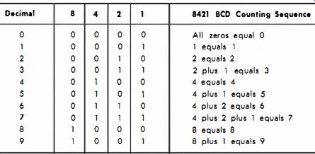
Table 4-1. 842 1 Binary Code
The 2*42 1 binary code derives its name from the numerical weighting assigned to each of the four "bit" positions in the code.
The 2* (two star) bit is called the real two and has a numerical weighting of two. The 2 bit also has a weighting of two, but is used only as an added value. The 2 bit is never used by itself, but only in combination with other bits in the code. The 2* bit is included in all combinations from two through nine.
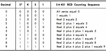
Table 4-2. 2*421 Binary Code
Logic and Logic Symbols
Fig. 4-1 is a schematic of an AND gate. If E1 and E2 are positive, Eo (output) will also be positive. If E1 or E2 is negative, Eo will be negative. In a typical system, E1 and E2 will be a nominal + 12 volts or -12 volts, and E will be 16 volts. Electron flow for such an AND gate is shown in Fig. 4-2, while the corresponding logic symbol is shown in Fig. 4-3.
A schematic of an OR gate is shown in Fig. 4-4. This gate is similar to an AND gate, except the diodes are reversed and E is a negative voltage. If either E1 or E2 is positive, output Eo will also be positive.
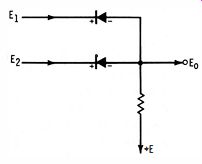
Fig. 4-1. Network for the positive AND gate.
If both E1 and E2 are negative, Eo will also be negative. Electron flow for this OR gate is shown in Fig. 4-5. The symbol for a positive-true OR gate with three inputs is shown in Fig. 4-6. NOTE : A negative-true
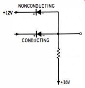
Fig. 4-2. Diagram of electron flow in an AND or gate network.
OR gate is shown in Fig. 4-7, and a negative-true AND gate is shown in Fig. 4-8.
Fig. 4-3. Symbol for an AND gate with three inputs.
In the dynamic AND gate shown in Fig. 4-9, voltage E can be either positive or negative and will inhibit or enable the gate, depending on the polarity of the applied voltage. If E is positive and a positive pulse appears at E1, the pulse will forward-bias the diode, and the output Eo will go positive. However, if E is negative, Eo will not go positive even though a positive pulse is at E1. The symbol for a dynamic AND gate is shown in Fig. 4-10. The dot is used to designate the enable leg (E in Fig. 4-9).
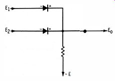
Fig. 4-4. Network for positive OR gate.
Fig. 4-11 shows the symbol for an inverter. Inverters are used to convert either a negative-going pulse to a positive pulse or a positive going pulse to a negative pulse.
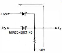
Fig. 4-5. Diagram of electron flow in an OR-gate network.
Fig. 4-12 shows a circuit combining an OR gate with an inverter. A positive pulse (12 volts) applied to one or more of the diodes in the OR gate will cause the output of the gate and E1 to switch to the same level. E2 will then become + 15 volts. This is sufficient to stop the
Fig. 4-6. Symbol for an OR gate with three inputs.
transistor from conducting and cause its output Eo to switch from plus 12 volts (the emitter potential) to minus 16 volts (the collector supply potential). Thus, for a positive 12-volt pulse input, the output will be a negative 16-volt pulse.
(A) Symbol. (b) Schematic.
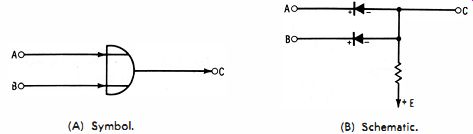
Fig. 4-7. Negative-true logic OR gate.
(A) Symbol. (B) Schematic.
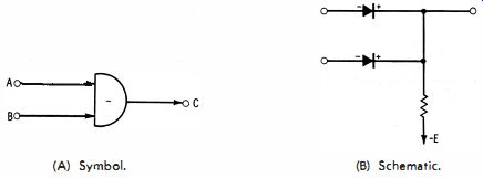
Fig. 4-8. Negative-true logic AND gate.
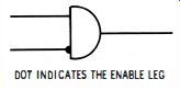
Fig. 4-10. Symbol for a dynamic AND gate.
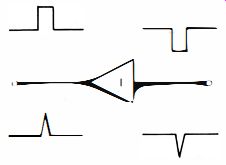
Fig. 4-11. Symbol and waveshapes for an inverter.
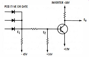
Fig. 4-12. Network for combination of OR gate and inverter.
Dynamic AND gates are often used in conjunction with flip-flops (bistable multivibrators) in digital circuits. Such an arrangement is shown in Fig. 4-13. When d-c power is first applied to the flip-flop, ...
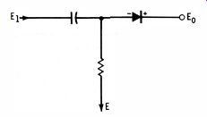
Fig. 4-9. Diagram for dynamic AND gate network.
... it immediately assumes a random state where one transistor or the other conducts and the second one is cut off. Which transistor will conduct is determined by inherent differences in components. If transistor Q2 is conducting and its collector is positive, the flip-flop is defined as having a "0." bit in it. Until there is a change in the flip-flop state, the circuit "stores" the 0 bit. When transistor Q1 is conducting and transistor Q2 is cut off, the flip-flop is defined as having a "1" bit in it.
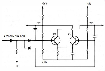
Fig. 4-13. Operational diagram for a flip-flop with a dynamic AND-gate input.
MODEL 880 DIGITAL MULTIMETER
The first instrument selected for discussion is manufactured by Electro Instruments, Inc., San Diego, California; it is designated as their Model 880. The instrument is designed to measure d-c voltages and ratios. Display is by means of Burroughs Nixie tubes mounted in a three-position, tiltable readout and consists of five digits, decimal point, and appropriate symbols for all measurements. A photograph of the unit is shown in Fig. 4- 14. Electrical outputs are also provided for remote operation of the instrument and for operation of an external printer or recorder. Operation is completely automatic. However, range selection may be manual if desired.
Basic Operational Theory
The meter is basically a device that measures d-c voltages by comparing the unknown d-c signal with a reference voltage from a digital register. The resulting potential difference is converted into information pulses which are used to continuously vary the contents of the digital register until a state of balance is achieved.
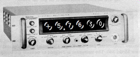
Fig. 4-14. Electro Instruments Model 880 digit.1 multimeter.
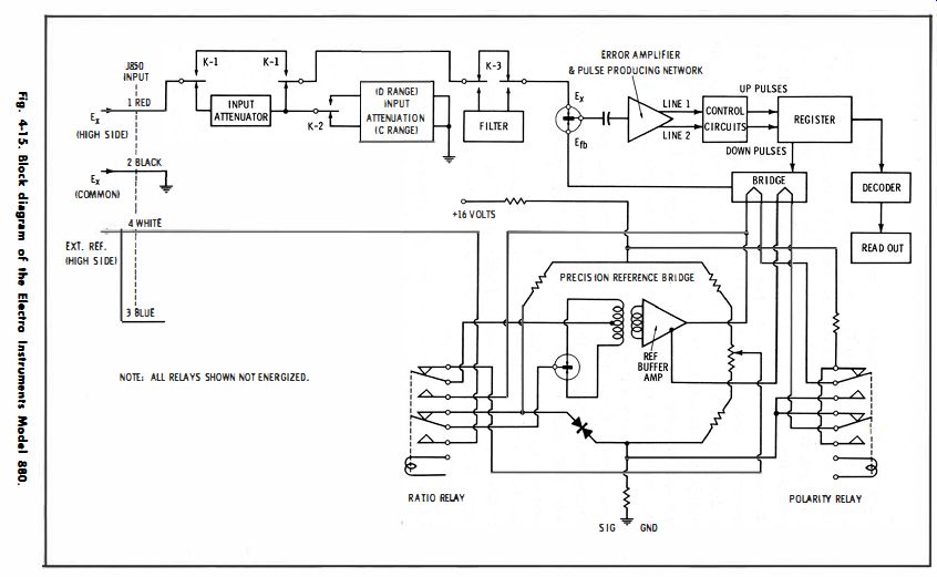
Fig. 4-15
The overall operational theory for the Model 880 can be divided into three parts : d-c voltage measurement, d-c ratio measurement, and print control operation.
DC Voltage Measurement--The unknown d-c signal, Ex, is applied to the instrument, and the input attenuator reduces this voltage to less than 10 volts. (See Fig. 4- 15.) The bridge feedback voltage (Efb) can never exceed 10 volts, as this is the value of the reference voltage. Therefore, it is necessary to reduce Ex to a value that can be equaled by Efb. A feedback voltage, Efb, is developed from a precision reference by a variable bridge circuit and applied to the other fixed contact on the chopper. The chopper continuously samples and compares Ex with Efb and applies the difference as a differentiated square wave to an error amplifier. The error circuit amplifies the differential output from the chopper, determines its polarity, and uses the resultant signals to generate further pulses. The polarity of the square wave, with respect to the position of the moving contact, determines whether these pulses will be directed on line 1 or line 2 to subsequent control circuits.
The control circuits consist of front panel switches and the following circuit boards : polarity, range gates, range flip-flops, and d-c ratio logic. The basic functions of these circuits are to convert the pulses arriving on line 1 or line 2 into up or down pulses and to provide control for ranging and polarity. Up pulses cause a digital register to increase both its count and the value of Efb; down pulses cause the register to decrease both its count and the value of Efb.
The digital register is a counter made up of five decades (units, tens, hundreds, thousands, and ten thousands) and is used to control a bridge and decoder circuit. The output from the bridge is Efb, the reference signal that is applied during the measuring cycle to one of the fixed contacts on the chopper.
Output signals from the register are converted by the decoders from binary-coded decimal (bed) into decimal form for readout presentation. The readout visually displays the digital equivalent of the unknown voltage after the meter has balanced.
A precision reference supply, working in conjunction with a reference buffer amplifier, provides a highly regulated ±10 volts d-c to the bridge. The reference signal can be positive or negative, depending on the state of a polarity relay.
DC Ratio Measurement-For d-c ratio measurements (see Fig. 4-1 5), the d-c voltage signals are applied to the instrument using three terminals on the input connector. Pin 4 is connected to the high side of the external 10-volt reference source, pin 1 to the high side of the unknown signal Ex, and pin 2 to the common of both the external reference and Ex.
With the Function switch set to the Ratio position, the ratio relay is energized and the polarity relay de-energized. The ratio relay disconnects the internal reference source and allows the external reference to be used as the voltage supply for the reference bridge. Instrument operation is the same as during d-c voltage measurements, but the meter now registers the ratio of the unknown d-c signal, Ex, to the external reference voltage.
Print-Control Operation--The meter is equipped with electrical output connectors and can be used to operate high input-impedance digital recorders, requiring ground on their selected lines. (See Fig. 4-16.) Print-control circuitry in the meter will provide a closed-loop timing system which operates independently of the recorder. On each measurement, after balance is achieved, a null-detector circuit sets a print control flip-flop. The output of this flip-flop is used to perform the following functions:
1. Provide a print command that can be used by a recorder.
2. Place a hold on the error amplifier so the meter will retain its last reading.
3. Trigger a scanner advance mono (monostable multivibrator) which provides a suitable delay time for a print cycle to take place.
4. Reset a noisy channel mono.
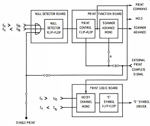
Fig. 4-16. Simplified block diagram of print control.
As the scanner advance mono returns to its rest state, it resets the print-control flip-flop so that the instrument will be able to perform its next measurement.
If, however, an external-print complete signal from a recorder or other external device is used to release the meter, the scanner advance mono will serve only as a scanner advance signal generator. For reliable operation, the external-print complete signal should be a 15-volt positive pulse with a maximum rise time of three microseconds and a minimum duration of five microseconds.
Circuit Analysis
The following paragraphs provide a detailed analysis of the Model 880 circuits. Because of the complex nature of the equipment, the circuits will be described in simplified form. Simplified schematics will be used in place of complete schematic diagrams wherever possible.
Signal Input Attenuation and Filtering Circuits
These circuits shown in Fig. 4-15 are straightforward and do not require detailed analysis. The high side of the unknown voltage is routed to K1 and/or K2 of the d-c voltage input circuits. There is no attenuation of the input signal Ex in the B range. In the C and D ranges, input attenuation circuits reduce the unknown d-c input signal to less than 10 volts . Relays K1 and K2 switch in the appropriate attenuation circuits. A 66-db attenuation filter is placed between relay K1 and the error-amplifier circuits. The filter is switched in or out of the circuit by relay Ka which is controlled by the positioning of the front panel Filter switch.
Error Amplifier and Pulse Network
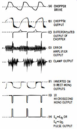
Fig. 4-17. Output waveforms of the pulse-producing network.
The chopper samples Ex and compares it with the feedback voltage (see Fig. 4-15). Its output is a symmetrical square wave with an amplitude representing the proportional difference between Ex and Etb and having a maximum amplitude 0.8 volts (waveform B in Fig. 4-17). This signal is applied to a differentiating circuit. If Ex is more negative than Eib, a series of positive pulses is produced by the differentiator (waveform C in Fig. 4-17). A smaller negative pulse (which is clamped out later) follows each positive pulse. If Ex is more positive than Efb, a series of negative pulses is obtained in the same manner.
The pulses from the differentiator are amplified by cascaded error and threshold amplifier circuits. The amplifier signals are then applied to a clamper for removal of the unwanted spikes produced by the differentiator circuits (waveform D of Fig. 3-17). The clamping circuit (Fig. 4-18) is controlled by the same signal that drives the chopper (waveform A of Fig. 4-17). The square-wave output signal from the chopper lags the chopper drive signal by approximately 90 deg.
This phase relationship enables the clamper to remove the pulse produced by the leading edge of the square wave and pass the pulse produced by the trailing edge (waveform E of Fig. 4-17). The pulse remaining at the output of the clamp circuit will be positive if Ex is positive with respect to Etb, and it will be negative if Ex is negative with respect to Etb. The clamp circuit output is used to drive a phase-splitter.
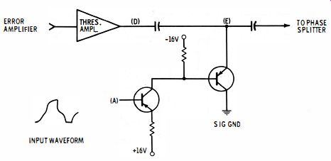
Fig. 4-18. Diagram of the operation of the clamp circuit.
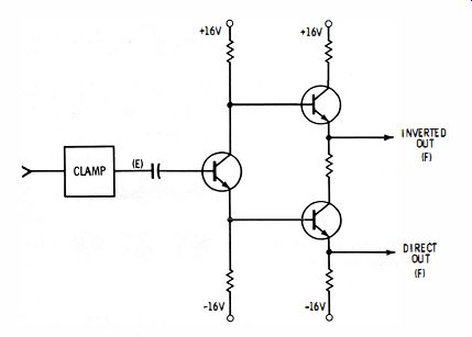
Fig. 4-19. Diagram of the operation of a phase-splitter circuit.
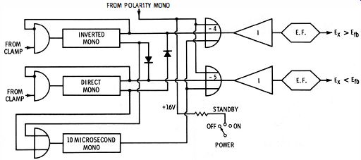
Fig. 4-20. Diagram of the operation of the mono circuits.
The function of the phase-splitter (Fig. 4-19) is to obtain two output signals of opposite phases from a single input. The two outputs of the phase splitter, one inverted and one direct, are coupled to the inverted and direct monos by dynamic AND gates 1 and 2. Both the inverted and direct monos are monostable multivibrators which require a positive pulse to trigger them.
When triggered, either the direct mono or the inverted mono then triggers a la-microsecond mono which produces negative output pulses of 10-microsecond duration (Fig. 4-20). The output of the three mono circuits and the output from a polarity mono (to be discussed later) are connected to the input terminals of negative OR gates in such a manner that OR gate 5 presents a negative la-microsecond pulse at its output, when triggered, and OR gate 4 presents a 10 microsecond negative pulse when the direct mono is triggered.
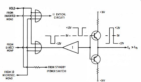
Fig. 4-21. Diagram of the operation of the emitter-follower circuits.
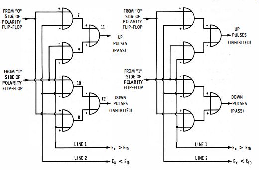
Fig. 4-22. Diagram of up-pulse or down-pulse determination.
Negative output pulses from OR gate 4, or, OR gate 5 are inverted in polarity and amplified by complemented emitter-follower circuits (Fig. 4-2 1). The amplified pulses designated as Ex > Efb from OR gate 4 are then routed to OR gate 6 (part of the print-command circuit null detector) and to OR gates 8 and 9 (Fig. 4-22). The amplified pulses designated as Ex < Efb from OR gate 5 are also routed to OR gates 7 and 10.
The pulse-producing network is disabled when OR gates 4 and 5 are inhibited by either one of the following conditions: (1) the positive pulse output of the polarity mono when the meter is undergoing a range change or polarity reversal and (2) a positive 16 volts from the Power switch when the meter is in Standby.
Meter sensitivity is controlled by varying the gain of the error amplifier with the front-panel Sensitivity control.
Determining Up or Down Pulses--If the input signal voltage is greater than the feedback voltage from the bridge of the register, Ex > Erb pulses are generated and routed by line 1 to OR gates 8 and 9.
(See Fig. 4-22.) The polarity flip-flop (which will be discussed later) has a zero in it when in a positive polarity state. (The polarity flip flop uses the basic flip-flop circuit previously discussed, Fig. 4- 13). With the polarity flip-flop in the zero condition, positive input is provided to OR gates 7 and 8, and negative input to OR gates 9 and 10.
These signals and the Ex > Erb pulses on line 1 cause OR gates 7, 8, and 9 to go positive. Having both inputs negative, OR gate 10 will have a negative output. Therefore, AND gate 11 is satisfied and positive pulses appear at its output. These are amplified by an emitter follower and emerge on the Up line as up pulses. AND gate 12, which is used to provide down pulses, is not satisfied at this time, as one of its inputs is negative.
If the input signal voltage is less than the feedback voltage from the bridge of the register, Ex < Erb pulses are generated and routed by line 2 to OR gates 7 and 10. The polarity flip-flop, still in a positive polarity state, continues to provide positive input to OR gates 7 and 8, and negative input to OR gates 9 and 10. These signals and the Ex < Erb pulses on line 2 cause OR gates 7, 8, and 10 to go positive.
OR gate 9, having both inputs negative, will have a negative output (Fig. 4-22). Therefore, AND gate 12 is satisfied, and positive pulses appear at its output. These are amplified by an emitter follower and emerge on the Down line as down pulses. AND gate 11 is not satisfied at this time, as one of its inputs is negative.
Effect of Up and Down Pulses on the Register--As shown in Fig. 4-15, both up and down pulses are applied to the register. This register is essentially a counter circuit that counts the pulses (in binary form) and holds the count for decoding (to decimal form) and readout (on the Nixie tubes). The register is made up of five decades (units, tens, hundreds, thousands, and ten thousands). In the standard Model 880, each decade contains flip-flop circuits that will count from zero to nine in the 2*42 1 binary code previously described. (The Model 880 can also be obtained with the binary count made in the 842 1 form.) In either event the decade flip-flops are similar to that shown in Fig. 4-13.
The up and down pulses are applied to the decades through the dynamic AND gate so that each successive pulse changes the count by 1. For example, if all of the counter flip-flops are at the 0 state, the first up pulse will switch the units decade flip-flop to 1. The flip-flop will remain in that condition until the next pulse. This action is continued until all of the flip-flops are set to the appropriate count (in binary form). In addition to counting (and holding) the pulses, the decade flip flops also control the nulling bridge, which is actually part of the decade and register circuitry. The meter seeks its null by switching resistors in or out of a bridge circuit which uses + 10 volts and ground for reference points. The bridge resistors are connected by transistor conduction to either a precision 10-volt reference supply or to ground, depending on the state of the corresponding flip-flops in the decade register.
The simplified resistor wiring for the bridge is shown in Fig. 4-23.
A typical bridge switching-circuit is shown in Fig. 4-24. Four such circuits are used in the units, tens, and hundreds decades (Fig. 4-25). In each decade the voltages across the resistors connected to the 2*, 4, 2, and 1 flip-flops are summed and applied to the chopper (as Etb)' Attenuation resistors, located between decades, reduce the effective voltage provided by a given decade to a value consistent with its significance in the counting sequence.
In operation (Figs. 4-23, 4-24, and 4-25), if the flip-flop is in its 0 state, the positive output from the 0 side forward-biases 01 to stop it from conducting. The output from the 1 side of the flip-flop being negative, back-biases a diode to allow 02 to be driven into conduction.
This effectively connects one end of the bridge resistor at the emitter of 02 to ground. If the flip-flop had been in a 1 state, the polarities of its output would be reversed. 02 would then be cut off, and 01 would conduct to connect the bridge resistor to the 10-volt precision reference supply.
As the flip-flops are moved to the appropriate count, the corresponding bridge resistors are switched in or out so that the bridge output equals that of the input voltage being measured. When this occurs, the chopper output is zero, and there are no further up or down pulses. All of the flip-flops and corresponding bridge resistors will remain in this condition unless the input voltage is changed.
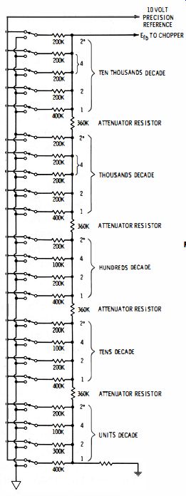
Fig. 4-23. Simplified diagram of resistor bridge network.
Therefore, the flip-flops have counted the pulses until each flip-flop in the corresponding decade is in a state (0 or 1) that represents the value of the input voltage (in binary form). The outputs of each flip flop in each decade must then be transformed from a binary code format to a decimal form suitable for presentation by the readout. This is accomplished by the decoder and readout circuits.
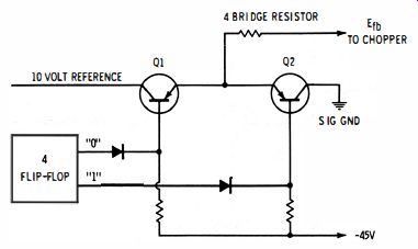
Fig. 4-24. Diagram of typical bridge switch.
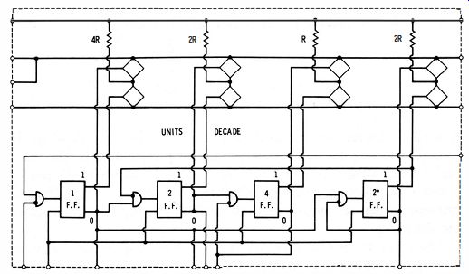
Fig. 4-25. Diagram of precision resistor switching of units, tens, and hundreds
decades.
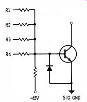
Fig. 4-26. Diagram of number 3 decoder.
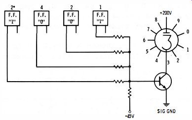
Fig. 4-27. Diagram of number 3 decoder operation.
Decoder and Readout Operation
The decoder circuits are primarily special combinations of resistor AND gates. A typical decoder is shown in Fig. 4-26. In operation the transistor conducts when its base is driven positive with respect to its emitter. The design of the circuit is such that the base will never go positive unless positive voltage is applied simultaneously to all four inputs at R1, R2, R3, and R4. Since these resistors are connected to the output terminals of four flip-flops in the decades of the register, the diode will conduct for only one of the nine possible states of the register.
Fig. 4-27 shows how the decoder is connected to the outputs of a typical decade. As can be seen, the collector of the decoder transistor is connected to the digit-3 Nixie indicator. In this example the decade is at count 3 and is providing positive outputs for a binary 2.
With the transistor driven into conduction, the full + 200-volt supply is applied to the Nixie, energizing the number 3. The circuit shown in Fig. 4-27 is used only in the ten-thousands decades. All other decades use the circuit shown in Fig. 4-28. Operation of this circuit (known as a biquinary decoder) is as follows. As before, the biquinary decoder is used to convert the binary-coded output of the four flip-flops in each decade to a decimal representation for presentation by the readout. Circuit design is such that two successive numbers (0 and 1, 2 and 3, etc.) are decoded by each of five resistive AND gates. Further processing then recognizes the state of the I-bit flip-flop to complete the decoding.
The Nixie driver transistor will conduct when both of the following two conditions exist: 1) the decoder gate output at the base terminal is positive and 2) the emitter line (corresponding to the selected odd or even number) is at a nominal ground potential through the odd and even select transistors (Qa and Qb). The ten cathodes of the Nixie indicator tube are connected to the collectors of ten corresponding driver transistors for a given decade. Thus, when a particular driver stage is conducting, the selected indicator cathode of the Nixie will glow as a result of the application of the full power-supply voltage (+250 volts) less the internal voltage drop of the tube from the anode to the selected cathode.
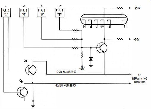
Fig. 4-28. Diagram of typical biquinary decoder stage.
Polarity Changing Operation
During d-c voltage measurements the polarity state existing in the meter is indicated by a plus or a minus symbol in the Nixie readout.
The symbol Nixie lamps are energized by Nixie driver circuits similar to those just described. Actual polarity-changing is controlled by the polarity flip-flop discussed earlier.
In operation, if the readout indicates a positive input and the polarity of the input signal is reversed to negative, the meter immediately senses that the input signal (Ex) is less than the feedback voltage (Etb). Down pulses are generated in the normal manner, and the decades in the readout are driven to +0.0000 with down pulses still being generated.
The down pulses are applied through a series of AND gates to trigger a polarity mono. The output of this polarity mono, which is normally negative when the mono is in its at-rest state, now goes positive and inhibits or places a hold on OR gates 4 and 5 in the pulse-producing network (Fig. 4-20). This prevents pulses that are still being generated by the chopper from passing through the gates and disturbing the digital register while polarity changing is taking place.
A pulse from the polarity mono also changes the state of the polarity flip-flop from 0 to a 1. The 0 output side of this flip-flop then goes negative, making the output from its 1 side positive. This reverses the polarity of the drive signals applied to the Nixie drivers and causes the negative-polarity symbol to be displayed. The symbol Nixie circuit is similar to the number Nixie circuits, except that it displays a symbol (+, -, R [ratio], E [voltage]) instead of numbers when the corresponding driver transistor conducts.
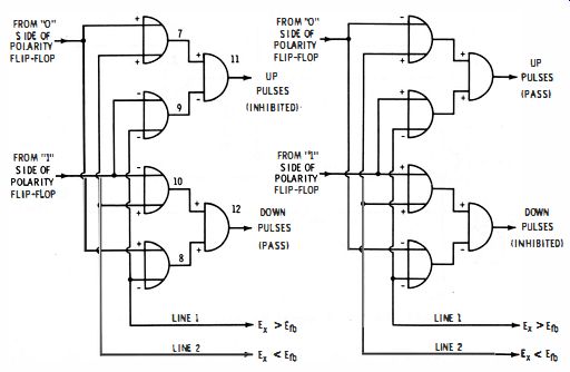
Fig. 4-29. Diagram of polarity-changing operation.
Fig. 4-29 shows operation of the gating circuits during a polarity change. When the polarity flip-flop changes state, AND gate 11 is enabled so that Ex < Efb pulses, which are still being generated by the chopper, can pass through the gate to the up-pulse line. At the same time a pulse, generated by the polarity flip-flop as it is changing state, passes through an OR gate that controls a bridge reference supply relay. When energized, this relay reverses the precision reference output of the bridge circuit so that -10 volts instead of + 10 volts is applied to the register bridge.
At this point the readout indicates -0.0000. As before, pulses are produced until the meter reaches a null and the readout is equal to the applied voltage. This operation is accomplished in the same manner as previously described for a positive input signal.
MODEL 111 DIGITAL VOLTMETER
The next instrument selected for discussion is manufactured by Simpson Electric Company, Chicago, Illinois, and is designated as their Model 111. The instrument is designed to measure d-c voltages.
Display is by means of seven individually lighted bars and is activated by 1-2-4-2 binary-coded logic from the internal counters. The display time is variable and can be controlled manually or from a remote location. A photograph of the unit is shown in Fig. 4-30.
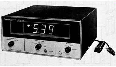
Fig. 4-30. Simpson Electric Company Model 111 digital meter.
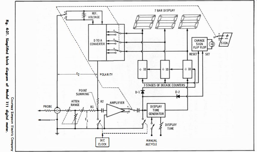
Fig. 4-31
Basic Operational Theory
The Model 111 is basically a null seeking-balancing system that samples a measured portion of the probe input voltage and compares it to an opposing voltage that is being developed internally (see Fig. 4-3 1). When both voltages are equal and opposite, the unit is said to be at equilibrium and a steady-state readout will exist at the counters.
In order to provide numerical readout the development of the internal voltage is divided into 1000 discrete steps (each step corresponding to a number between 000 and 999). As this voltage increases by its 1/1000 increments until equilibrium of the counters scale is attained.
The three stages of decade counters provide the 1000 possible output states of 000 to 999. A seven-bar display is connected to each of the decades to provide the readout of the 1-2-4-2 logic in each of the counters . The counters also drive the digital-to-analog converter which divides a reference voltage into 1000 steps. At the count of 000, the digital-to-analog converter output is zero volts. At the count of 999, the output has increased to approximately five volts. As the counters scale from 000 to 999 (because of added pulses), the output of the digital-to-analog converter (consisting of a staircase waveform) is increased by 1/1000 of the reference voltage (per pulse). Because no more than one second is required to achieve balance, the counter input repetition frequency becomes 1 khz, which in turn becomes the clock rate of the instrument.
The polarity switch reverses the output sense of the digital-to-analog converter. That is, a negative-going staircase is generated when a positive voltage is measured. Conversely, a measured negative voltage results in a positive-going staircase.
When the counters are in the 000 state, the digital-to-analog converter output voltage (E2) is zero. When E:l and a positive input voltage (E1) are applied to the summing network (Rt and R2), a positive voltage representing an out-of-balance signal appears at the summing point.
The clock period of one millisecond is divided into two parts.
During the first part (approximately 500 microseconds), grounding switches at the input and output of the amplifier are closed, causing a no-signal condition at the counters and allowing the input and output capacitors to charge to their steady-state values. During the second part of the clock period the switches open, allowing the positive out-of-balance signal to be amplified as a positive-going pulse.
The series diode D1 passes this pulse to the counters, causing a count of 00 1 to appear. This causes the output of the digital-to-analog converter to go negative by 1/1000 of the reference voltage. This completes the action of the first clock-pulse period.
The process is duplicated again in the second clock period. During the first part of the second period the switches are closed to establish 0-volt reference. In the second part of this period, they are opened, and a positive out-of-balance signal condition at the summing point will then initiate another count. The meter will try again for balance.
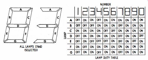
Fig. 4-32. Diagram of seven-bar lamp display arrangement.
If the voltage to be measured is in range, then at some count between 000 and 999, a null or slightly negative voltage will be obtained at the summing point. At this time, more pulses can pass to the counters through Db and the meter reaches equilibrium.
At equilibrium, the display time generator starts its functions to hold the final-state displays of the counter for a time, depending on the setting of the display time control and/or manual recycle button. It also (not shown in Fig. 4-31) locks out pulses from the amplifier so that stray noise spikes or removal of the probe will not cause spurious readings. At the end of the display cycle, the counters are reset, and the meter repeats the entire cycle just described.
In the case of a wrong-polarity input signal, a negative-going pulse will appear at the output of the amplifier during the second half-cycle of the first sampling period (counters at 000). D1 prevents them from counting. However, the other diode (D2) passes the negative pulse and triggers the change-sign flip-flop. This lights the Change-Sign lamp. Reversing the polarity switch reverses the sense of the digital-to-analog converter output and the sense of the amplifier output, so that a negative out-of-balance signal at the summing point will initiate a count, and each count will produce a positive step at the digital-to-analog converter output.
Fig. 4-32 shows the seven-bar display arrangement. The seven bars are arranged to form numerals. Any number from zero through nine can be formed with the proper combination of bars. For example, to form the number 3, lamps B and E do not light, but the remaining lamps, A, D, G, C, and F, do light. The lamps are turned on or off by driver transistors which, in turn, are controlled by the decade counter flip-flop circuits. Each of the three numerals is provided with a separate seven-bar display.