AMAZON multi-meters discounts AMAZON oscilloscope discounts
Rectification is the basic property of the diode, therefore, diodes are useful in all applications demanding simple conversion of AC to DC. Conventional small-signal diodes, unlike semiconductor power rectifiers, are low-power devices which cannot safely handle more than a few hundred milliwatts at the most. But where only low power is involved, the conventional diode is entirely adequate as a rectifier and, at the same time, is smaller and cheaper than a power rectifier. It lends itself well to subminiature power supplies for transistorized equipment, photoconductive cells, varactors, and thermistors.
In addition to AC rectification, voltage regulation is afforded by diodes-principally the zener diode. This is made possible by the nonlinear conductance of the unit. Unilateral conductivity of the diode also may be used, as in the application shown in Fig. 4-8.
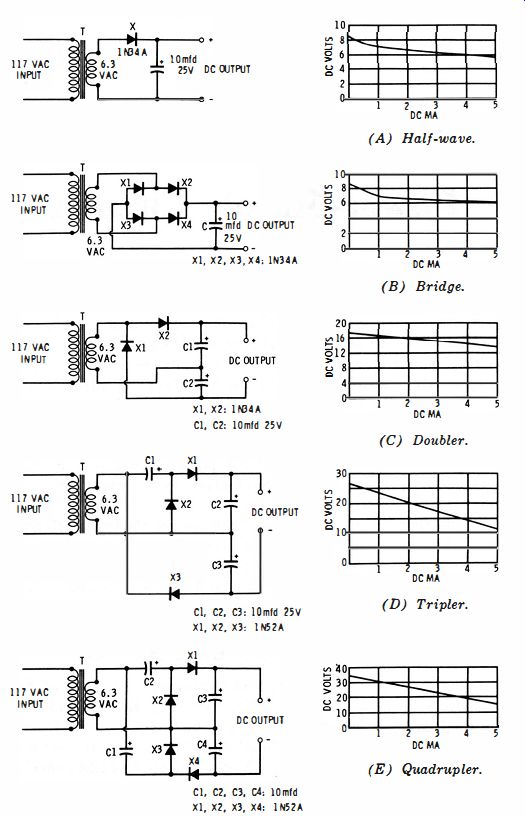
Fig. 4-1. Low-level DC power supplies.
FIVE LOW-LEVEL DC POWER SUPPLIES
Fig. 4-1 shows the circuits and performance curves of five miniature AC line-operated DC power supplies suitable for the operation of low-power devices, such as photoconductive cells, varactors, and conventional transistors, and for supplying fixed bias for tube circuits. Each of these circuits operates on 6.3 volts AC delivered by a small 1.2-ampere filament transformer (T) . Higher-voltage secondaries (for example, up to 24 volts) may be used with proportionately higher DC output, provided higher-voltage capacitors are substituted for those shown. The volt-ampere curves show the DC output voltage delivered by each of these circuits at various currents up to 5 milliamperes.
Half-Wave
Fig. 4-1A shows a simple, single-phase half-wave supply. A single 1N34A general-purpose germanium diode (X) is the rectifier. The no-load DC output is equal to the peak value of the 6.3-volts AC input minus the small forward voltage drop in the diode, and is approximately 8.5 volts. This drops to approximately 6 volts at 5 ma. The output ripple is low enough for most applications ; however, additional filtration may be obtained by adding a 10-henry choke and 10-mfd capacitor.
Bridge
Fig. 4-1B shows a full-wave bridge rectifier employing four 1N34A general-purpose germanium diodes. The no-load and full-load DC output is the same as for the half-wave circuit, but the ripple frequency is twice that of the power line.
Doubler
Fig. 4-1C shows a voltage-doubler circuit. This circuit delivers a no-load DC output that is more than double the AC input voltage-it is equal to two times the peak value of the AC voltage, or approximately 17.7 volts for 6.3 volts rms input.
This drops to approximately 13 volts at 5 ma load. Two 1N34A general-purpose germanium diodes are used in this circuit.
Tripier
Fig. 4-1D shows a voltage-tripler circuit. This circuit actually delivers a no-load DC output voltage that is more than triple the AC input voltage--it is 3 times the peak value of the AC voltage, or approximately 26.7 volts for 6.3 volts rms input.
This drops to approximately 13 volts at 5 ma load. Three 1N52A general-purpose germanium diodes having increased peak inverse voltage ratings, are used in this circuit.
Quadrupler
Fig. 4-1E shows a voltage-quadrupler circuit that delivers a no-load DC output voltage which more than quadruples the
AC input voltage-it is four times the peak value of the AC voltage, or approximately 35.5 volts for 6.3 volts rms input.
This drops to approximately 14.5 volts at 5 ma load. Four 1N52A general-purpose germanium diodes are used in this circuit.
CONVENTIONAL DIODE VOLTAGE REGULATOR
The nonlinear forward conductance of a germanium diode at low current levels may be used to stabilize a low DC output voltage against excursions of the DC input voltage. With conventional small-signal diodes, this scheme is practical only when the current drawn from the circuit by an external load is a small percentage of that flowing through the diode.
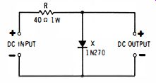
Fig. 4-2. Conventional-diode voltage regulator.
Fig. 4-2 shows the regulator circuit. The DC input voltage is obtained from a power supply or battery. Resistance R is chosen to set the forward current through diode X to the center of the steepest portion of the diode forward-conduction curve. DC output voltage is taken across the diode. As the input voltage changes, the diode current changes proportionately.
But because of the steepness of the curve, the voltage across the diode changes only slightly for a large increase or decrease in current. Thus, the output voltage changes only slightly, although the input voltage fluctuates considerably.
As the output load current approaches the diode current in magnitude, the regulation becomes poorer, since increasingly more current flows through the load and is not subject to control by the diode.
Because of the voltage-divider action of R and X in series, the output voltage is less than the input voltage. Therefore the input voltage must be properly selected, if a given output voltage is to be realized. This regulator is basically a low voltage scheme, since the most usable portion of the forward current of a conventional germanium diode lies between 0.05 and 0.2 volt.
Practical constants for the circuit shown in Fig. 4-2 are: R is a 40-ohm, 1-watt resistor; and X is a IN270 gold-bonded germanium diode. At 1 volt input, the diode current is 10 ma and output voltage is 0.6 volt ; at 3 volts input, the diode current rises to 50 ma, but the output voltage increases only to 1 volt. Thus, the output voltage changes only 1.67 time for an input voltage change of three times.
TWO ZENER-DIODE REGULATOR CIRCUITS
Zener diodes, because of their lower internal resistance and steeper curve at the operating point, provide considerably better voltage regulation than the conventional diode circuit shown in Fig. 4-2. Fig. 4-3 shows two regulator circuits using these more expensive diodes.
(A) DC circuit. (B) AC circuit.
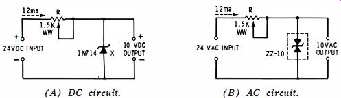
Fig. 4-3. Zener diode voltage regulators.
In the DC regulator (Fig. 4-3A), a 1N714 diode is reverse biased to its zener point by 12 ma of current flowing from the 24-volt DC supply through limiting rheostat R. (The latter is initially set for this value of current.) The input voltage can change several hundred percent without changing the 10-volt output by more than a few percent in the same direction. The reason for this is the steep slope of the reverse conduction curve within the zener region of the diode (a small change in applied voltage produces a large change in reverse current, and vice versa) . Zener-type regulators are ideally suited for regulation of low voltages. Other devices, such as gaseous tubes, are available for higher voltages ; however, several zener diodes may be connected in series to regulate a multiple of the single-diode voltage. Higher-voltage and higher-current diodes than the one shown in Fig. 4-3A are also available.
The AC regulator (Fig. 4-3B) employs a ZZ-10 double-anode zener diode. (Two separate zener diodes may also be connected, back-to-back, for this purpose.) This arrangement holds each peak of the AC output voltage to 10 volts, resulting in a squared output wave.
In this circuit, as in the DC regulator previously described, current-limiting rheostat R is set for a diode current of 12 ma.
Double-anode zener diodes are available with higher voltage and current ratings than the unit shown in Fig. 4-3B.
ZENER DIODE AS REFERENCE ELEMENT
Because the zener diode will deliver a constant DC voltage in a suitable circuit, it may be used as the DC reference source in a transistor-type regulated power supply. In tube-type supplies this function usually is performed by a gaseous regulator tube, but a series string of zener diodes may be used.
Heat Sink
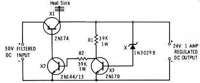
Fig. 4-4. Zener diode as reference element.
In Fig. 4-4, X is a 1N3029B zener diode used as the DC reference for transistor X3. Transistors X2 and X3 constitute a DC amplifier which receives its input signal from diode X and delivers its output signal to transistor X1. X1 is connected between the +DC input terminal and +DC output terminal, acting as a series resistor. Its resistance is controlled by current fed from the + DC output terminal back to its base.
Thus, when the output voltage rises, the resistance of X1 is increased, and this reduces the output to its initial level. This action is accomplished in the following manner : normally X acts as an extremely high resistance, permitting almost no current to flow into the base of X3. When the voltage at the +DC output terminal exceeds the zener point (24 volts), how-ever, the diode conducts, and this current is amplified by X3 and X2, in that order, and applied to X1. This increases the resistance of X1 and pulls the output back to 24 volts.
This supply delivers 24 volts DC at 1 ampere. The output voltage is regulated within 1%.
ZENER DIODE AS VOLTAGE STANDARD
The constant voltage drop across a zener diode may be used as an accurate standard voltage for instrument calibration and the accurate biasing of electronic circuits. Because the zener diode is a silicon unit, its temperature characteristics are good and the voltage may be relied on within ±5% when only the diode current is controlled, and to a much closer tolerance when the voltage is initially checked with an accurate voltmeter.
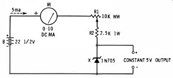
Fig. 4-5. Zener diode as voltage standard.
Fig. 4-5 shows a DC voltage-standard circuit employing a 1N705 zener diode. The output is 5 volts when the current, as read with milliammeter M, is set to 5 ma by adjustment of rheostat R1. While a battery is shown for maximum portability, the input voltage may be obtained also from a rectifier-type power supply.
A standard AC voltage may be obtained with a circuit such as the one shown in Fig. 4-3B, provided an AC milliammeter is inserted for setting the current to the zener level of 12 ma.
This type of standard is often used as an oscilloscope voltage calibrator.
These circuits are designed for low voltage output, but higher standard voltages may be obtained with zener diodes having higher voltage rating, or by operating a suitable number of zener diodes in series.
DC BIAS SUPPLY
Fig. 4-6 shows the circuit of a compact and inexpensive DC unit for supplying fixed bias to tubes in a radio or TV receiver or audio amplifier. Filtered output voltages are -1, -2, -3, -5, and -8.5 volts.
The AC input power is taken from the 6.3-volt filament (heater) winding of the power transformer in the receiver or amplifier. Since this bias supply draws only 170 microamperes, it will not upset the filament circuit. The AC is rectified by a 1N34A general-purpose germanium diode (X) . (At the powerline frequency, a small selenium diode also might be used.) The DC is filtered by C1, C2, and R1. A 50,000-ohm voltage divider (R2 to R6) supplies the five bias voltages. If a 50,000-ohm wirewound resistor with sliding clips is used, the clips may be set to the various voltages shown (or to any other desired values) with the aid of a DC VTVM. If fixed resistors are used, the odd values are made up as follows ; R2 = 15K + 5.6K, R3 = 11K + 750 ohms, R4 = 5.6K + 300 ohms, R5 = 5.1K + 750 ohms, and R6 = 5.6K + 300 ohms. All resistors are one half watt.
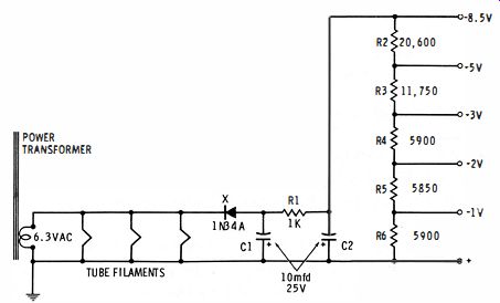
Fig. 4-6. DC bias supply.
FREE-POWER SUPPLY
Fig. 4-7 shows the circuit of a free-power supply which delivers DC voltage for operating transistors and other low-current devices. It is so called because the power is taken from the air at no cost to the user.
This supply is essentially a broadcast-band crystal receiver tunable from 540 to 1,600 khz. The DC output current of the 1N279 high-conductance germanium diode (X) develops the DC output voltage across 1,000-ohm resistor R. Capacitor C2 effectively bypasses the audio modulation in the received signal, rendering the output voltage a smooth DC.
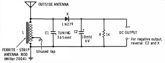
Fig. 4-7. Free-power supply.
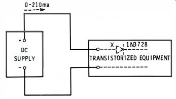
Fig. 4-8. DC protector for transistorized circuits.
The output voltage magnitude depends upon the strength of the received signal. For highest output, therefore, the strongest and/or nearest local broadcast station should be tuned in. A good outside antenna and ground are essential.
DC PROTECTOR FOR TRANSISTOR CIRCUITS
Some transistors are sensitive to power-supply polarity and may be damaged if the supply polarity is reversed. Fig. 4-8 shows how a diode may be connected as a one-way valve in series with the DC supply line within the transistorized equipment to prevent such damage.
Here, X is a 1N3728 subminiature silicon diode. Its polarity in the circuit is such that it passes forward current into the equipment. If the power supply inadvertently is reversed, the diode is then polarized for reverse current, which for the silicon diode is so tiny that the power supply may be considered to have been switched off.
This switching action is instantaneous and very effective.
The diode will pass as much as 210 ma to the equipment at a maximum voltage loss of only 1.1 volts across the diode (the power-supply voltage may be increased by this amount) . This will be sufficient for some power transistors, as well as all small-signal types. When the polarity is reversed, the diode resistance becomes more than 5,000 megohms. This is equivalent to an open switch, since with a 20-volt supply the current flowing into the equipment is less than 0.004 microampere.
For operating currents higher than 210 ma, heavier-duty silicon diodes may be used with comparable results.
DIODE IN TRANSISTOR BIAS NETWORK
For maximum stability, a stiff voltage divider, operated from the main power supply, is used to furnish DC base bias to a common-emitter-connected transistor. If a zener diode biased to its zener region is used as the bottom section of the divider, the regulating property of this type of diode will provide a stable bias voltage.
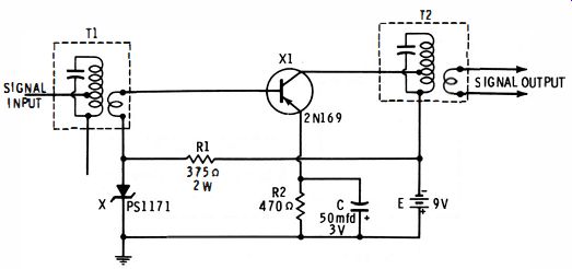
Fig. 4-9. Diode in transistor bias network.
In Fig. 4-9, resistor R1 and zener diode X form the bias voltage divider. Resistance R1 must be chosen with respect to the power supply voltage (E) so that zener current will flow through the diode. The zener voltage of the diode must be the same as the desired base-bias voltage. Thus, in the IF amplifier, Fig. 4-9, X is a PS1171 diode which has a zener voltage of 1.5 volts, R is 375 ohms 2 watts, and E is 9 volts. Because of its low dynamic impedance (9 ohms), the diode does not need a bypass capacitor.
The cost of the increased stability provided by this bias scheme is the relatively high current which must be supplied to the diode (5 to 20 ma, depending on diode type). But where high stability is imperative, this is a simple, inexpensive method.
RELAY RECTIFIER
To eliminate the nuisance of batteries in some installations, it sometimes is desired to operate a sensitive DC relay from the AC power line. Fig. 4-10 shows a miniature power supply for this purpose.
The 6.3-volt output of a small filament transformer (T) is rectified by a 1N281 high-conductance germanium diode (X) and filtered by C1, C2, R1 and R2. Switch S2 represents the contacting device normally used to operate the relay.
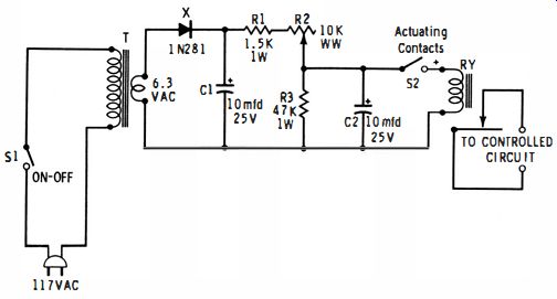
Fig. 4-10. Relay rectifier.
Rheostat R2 is set to the point at which the relay picks up firmly when S2 is closed. For maximum response speed, no capacitor is permanently connected across the relay coil. The relay may be any one of the available sensitive DC types in the range 100 microamperes to 2 milliamperes and having coil resistance between 100 and 5,000 ohms (Table 5-2, Section 5). For lower relay currents, select a higher maximum resistance for R2.