AMAZON multi-meters discounts AMAZON oscilloscope discounts
Vacuum-tube voltage regulators have equivalents in solid-state circuitry. Both open-loop and closed-loop regulation is used, depending on the amount of variation that can be tolerated in the power-supply output. Shunt and series circuits have been developed.
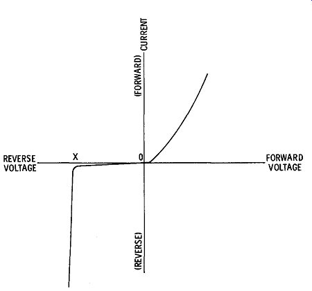
FIG. 1. Zener-diode electrical characteristics.
OPEN-LOOP OPERATION
Earlier in this guide it was pointed out that, by the use of a gas-filled shunt-regulator tube, the d-c output of a power supply can be held to within quite close limits in spite of variations in load current and sup ply voltage. There exists a solid-state equivalent of the gas-filled voltage-regulator tube-the zener diode. Before examining the basic zener regulator circuit, it is necessary to understand the operation of the zener diode itself.
FIG. 1 is the characteristic curve of a typical zener diode. Notice that as the reverse voltage applied to the diode is increased from zero to point X, there is negligible reverse current through the diode. When the voltage is increased beyond point X, the reverse current suddenly increases. At this point, electrical activity in the diode "avalanches," and the reverse current increases rapidly, although there is only a small increase in reverse voltage. In other words, the voltage drop across the zener diode remains practically constant for wide variations in current. As you can see, this characteristic of the zener diode is very similar to that of the gas-filled voltage-regulator tube when the latter ionizes.
FIG. 2 shows a zener diode connected to a source of variable voltage. Note that the polarity is such that the diode blocks the flow of electrons. A resistor is placed in series with the zener diode to limit the current through the diode to a safe value when it avalanches. As the voltage from the potentiometer (through the current-limiting re-sis tor) is increased, the voltage across the diode also increases. When the applied voltage reaches the avalanche voltage, the diode will con duct ( in the reverse direction from normal conduction). As the applied voltage is raised still further, the voltage across the diode re mains constant. The series resistor limits the current through the diode to a value that does not exceed the power-dissipation rating of the diode.
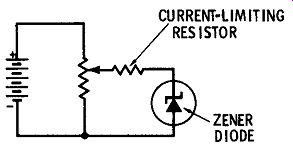
FIG. 2. Operation of a zener diode.
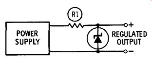
FIG. 3. Basic zener-diode voltage regulator.
From this explanation you can see that the zener diode acts like a variable resistor, the resistance increasing or decreasing, as required, to maintain a constant voltage drop in spite of varying current. It functions in a manner similar to the gas-filled voltage regulator.
FIG. 3 shows the zener diode used as a shunt regulator in a power supply circuit. To examine briefly its operation, assume that the load connected to the output of the regulator draws an increasing amount of current. This results in a greater voltage drop across current-limiting resistor R1 and a smaller voltage drop across the diode. The diode will then pass less current, the voltage drop across the current-limiting resistor will be reduced, and the voltage applied to the load will come back up to its original value.
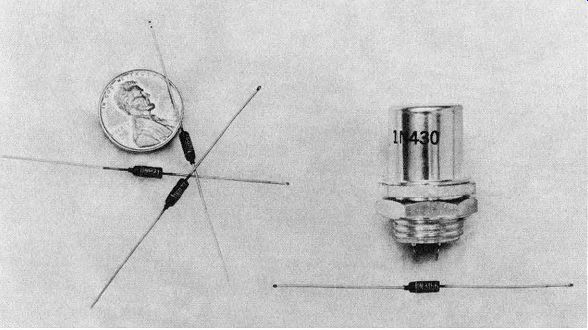
Courtesy Motorola Semiconductor Products, Inc. Typical zener diodes of varying capabilities for use as reference-voltage sources.
Should the load current decrease, there will be a smaller voltage drop across the current-limiting resistor, tending to raise the voltage across the zener diode. This will increase the current through the diode, thereby increasing the voltage drop across R1. As a result, the voltage across the load will drop back to its original value.
Zener diodes are available in a much wider range of operating voltages than are gas-filled voltage regulators. The latter can be purchased in ranges from 75 to 150 volts. The low voltage limit on these tubes is due to the fact that the gas used in them will not ionize below approximately 75 volts. Zener diodes, which do not depend on the ionization of gas for their operation, may be obtained with operating voltages as low as several volts and as high as several hundred volts.
Zener diodes are also available in a much wider range of operating currents than are tube-type voltage regulators. The typical gas-filled unit has a recommended operating current of 40 ma. In contrast, zener diodes are available in operating currents ranging from several milliamperes for reference-voltage units to several hundred milliamperes for the high-power units.
In all voltage-regulator circuits, a supply voltage is required that is somewhat higher than the actual value of the regulated voltage. The reason for this is that there is a voltage drop across the current-limiting resistor.
The approximate value of the current-limiting resistor needed for use in a zener-diode shunt voltage-regulator circuit can be found by the following formula: R = Es - ET I
where, R is the value of the current-limiting resistor, in ohms, Es is the unregulated supply voltage, in volts, ET is the value of the regulated (zener) voltage, in volts, I is the maximum zener-diode current (no-load), in amperes.
This formula does not take into account the effects of elevated temperature and other variables on the zener diode. Nevertheless it is sufficient to place the resistance value "in the ball park" and is adequate for most experimental projects.
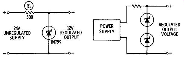
FIG. 4. "Add-on" zener voltage regulator. FIG. 5. Two zener diodes
connected in series.
FIG. 4 is the schematic of a simple "add-on" zener-diode voltage regulator that can be connected to the unregulated output of a 24-volt power supply to yield a regulated output of 12 volts. The unregulated voltage is applied to the zener diode via current-limiting resistor R1.
The value of this resistor is selected to provide the rated no-load current through the zener diode ( 30 ma). The values given in FIG. 4 are for a specific zener-diode type and supply voltage; however, a zener diode with a different rating may be substituted for the one shown to obtain a different value of regulated voltage. The value of series-dropping resistor will have to be changed if a different diode is used.
Like their regulator-tube counterparts, zener diodes may be connected in series to raise the total regulated voltage, as shown in FIG. 5. When zener diodes are used in this manner, care should be taken to select units of identical power ratings.
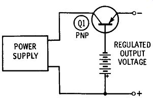
FIG. 6. Basic closed-loop voltage regulator.
CLOSED-LOOP OPERATION
The basic circuitry of solid-state closed-loop voltage regulators is essentially the same as that of their vacuum-tube counterparts.
Regulation is achieved by comparing the change in output voltage of the power supply with a fixed reference voltage. The resulting error signal is then used to actuate a control device in such a way as to either increase or decrease the current through it; this change brings the load voltage back to its original value.
FIG. 6 shows perhaps the simplest of all closed-loop semiconductor voltage regulators. In operation, the collector and emitter of transistor Q1 are connected in series between one side of the unregulated voltage and the load. The base-to-emitter bias consists of battery M1 plus the voltage drop across the load. The size of the battery is selected in such a manner that the algebraic sum of the battery voltage and the desired load voltage will give a suitable base-to-emitter (base-bias) voltage.
When the load voltage changes, the base bias of the transistor also changes. The difference between this resultant base bias and the normal bias is called the error signal. If the load voltage decreases, the error signal changes the bias so the transistor conducts less current.
A smaller voltage drop across the transistor results in a higher voltage across the load, so normal operation is restored.
FIG. 7 shows the same basic circuit, except that the reference battery has been replaced with a zener diode which furnishes the required reference voltage.
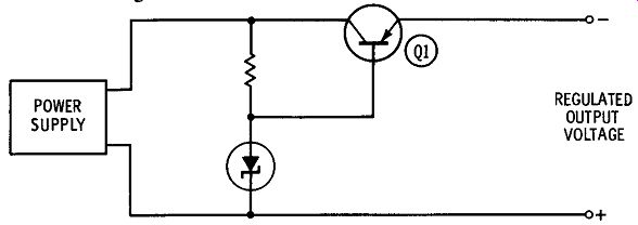
FIG. 7. Use of zener diode to provide reference voltage.
The circuits shown in Figs. 6-6 and 6-7 employ a series-regulator transistor (Q1 ) as the current-controlling element. The circuit of FIG. 8 makes use of a shunt regulator (Q1) . This configuration differs from the series regulator in that the regulating element is in parallel with the load. In operation, Q1 shunts more or less of the current through resistor R1, the amount depending on the load-current variations. In this circuit zener diode X1 provides the required reference voltage for the base of Q1.
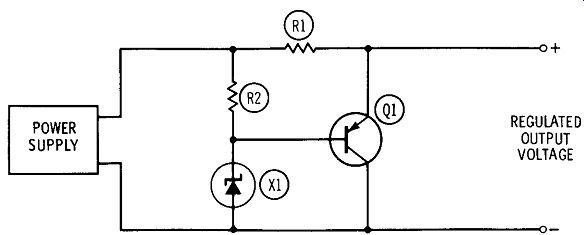
FIG. 8. Basic shunt voltage regulator.
The choice between the series and shunt voltage regulator is largely determined by the value of load current. Operation of the shunt regulator is such that under conditions of little or no load, the control element, Q1, must conduct the entire load current. As the external load current is increased, Q1 conducts less current, drawing the least current at full external load.
On the other hand, the series-regulator element dissipates the least amount of power at zero load conditions. As the external load is increased, current through the regulator and its dissipation increase.
Thus, the shunt regulator is best suited for conditions where nearly maximum load current will be drawn most of the time, and the series regulator is best for light-load conditions.
One advantage of the shunt regulator is that it is protection against short circuits in the load. As you can see from FIG. 8, Q1 is connected directly across the external load. Should the load become short circuited, all that will happen is that operating voltage will be removed from Q1. In the case of the series regulator, however ( FIG. 6), a shorted external load will cause an excessive current through Q1 and this current will probably destroy Q1. A Typical Power Supply FIG. 9 is the schematic of a handy variable-output voltage-regulated power supply that can provide an output-voltage range of 6 to 25 volts at a maximum current rating of I ampere. The voltage appearing across the secondary of T1 is rectified by X1, X2, X3, and X4 in a bridge-rectifier configuration. The output from the filter is applied to the collector of transistor Q1. The emitter of Q1 is connected to the negative output terminal. Zener diode XS and current limiting resistor R1 provide the reference voltage for the base of Q1.
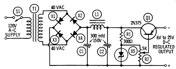
FIG. 9. Variable-voltage regulated power supply.
----------- Parts List for FIG. 9
Item No. Description
C1 Capacitor, 300 mfd, 150 volts, electrolytic
C2 Capacitor, 300 mfd, 150 volts, electrolytic
L Choke, .035 hy, 1 amp (Knight 54D2343, or equivalent)
Q1 Transistor, PNP, 2N375
R1 Resistor, 300 ohms, 1 watt
R2 Resistor, variable, 5000 ohms
SL Switch, spst
T1 Transformer, power, 40 volts, 1 amp (Knight 54D4735, or equivalent)
X1 Rectifier, silicon, 1N2482
X2 Rectifier, silicon, 1 N2482
X3 Rectifier, silicon, 1 N2482
X4 Rectifier, silicon, 1 N2482
X5 Diode, zener, 1 N921
--------------
The stabilized voltage appearing across XS is applied to voltage-con trol potentiometer R2, the slider of which is connected to the base of Q1. Thus, by adjusting R2, the amount of base bias applied to Q1 can be varied, and the value of the regulated output voltage changes.
Series control transistor Q1 should be provided with a suitable heat sink in this circuit. The case of Q1 must be insulated from the chassis; this can be accomplished as shown in FIG. 10. When this regulated power supply is used, extreme care must be taken not to short-circuit its output terminals because this will quickly destroy the transistor.
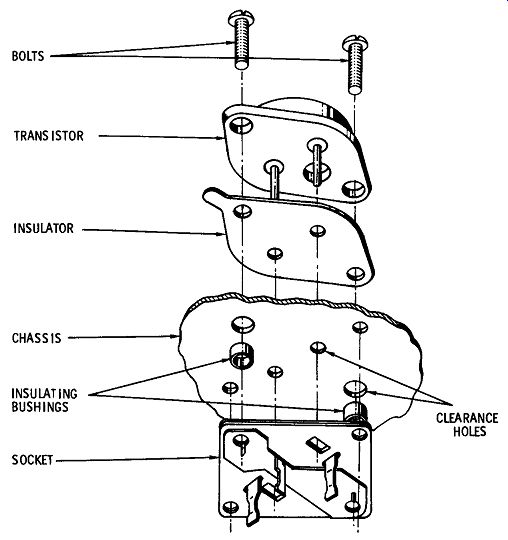
FIG. 10. Mounting of power transistors.
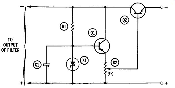
FIG. 11. Improved series regulator.
An Improved Regulator
While the basic series voltage regulator employed in the power sup ply described previously will provide a voltage regulation on the order of 1.5 % for extreme changes in load current, there is room for improvement in the basic circuit. Take a look at FIG. 11. Notice that transistor Q1, connected as an emitter follower, is placed between the output of the zener diode and base of the series-control transistor, Q2.
The purpose of Q1 is to amplify the error signal obtained by comparing the regulated voltage from X1 with the unregulated voltage. The emitter of Q1 is connected to the base of series-control transistor Q2 through potentiometer R2.
Ripple Reduction
Notice that capacitor C1 is connected across the zener diode in the circuit of FIG. 11. The presence of this capacitor greatly reduces the ripple in the regulator output. Placed in the base circuit of Q1, C1 has an effective value roughly equal to its capacitance times the beta of Q1. Thus, if C1 has a capacitance of 1000 mfd and Q1 has a d-c beta of 50, the effective value of C1 will be 50,000 mfd.
This electronic filtering action can be put to good use in reducing the ripple output of an unregulated power supply, as shown in Fig. 12. Although this filter does not provide regulation, it is very effective in reducing the ripple. This circuit can be added to the output of a low-voltage (up to 24 volts) power supply to greatly reduce the ripple content of the output.
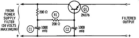
FIG. 12. Simple electronic filter.
In operation, Q1 is connected in series between the negative terminal of the power supply and the negative output terminal of the electronic filter. C1, R1, and C2 form a pi-section filter, applying ripple free base bias to Q1. Any ripple appearing on the collector of Q1 is smoothed out so that almost none appears on the emitter of Q1. This is due to the amplifying action of Q1.
When this electronic filter is used, care must be taken not to short circuit the output terminals because this will destroy Q1. Also, the power supply feeding the electronic filter must have some filtering built into it-at least a 100-mfd capacitor across its output terminals.
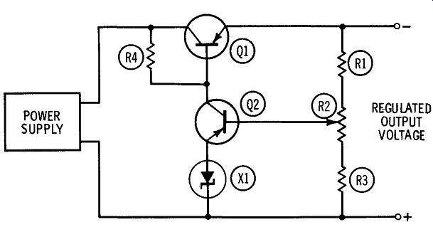
FIG. 13. Modified series voltage regulator.
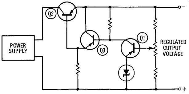
FIG. 14. Closed-loop series voltage regulator with two-stage error-signal
amplifier.
Other Regulator Circuits
FIG. 13 shows another type of closed-loop regulator circuit. Notice that it is quite similar to one discussed in an earlier chapter dealing with vacuum-tube types.
The operation of the regulator shown in FIG. 13 is as follows.
When the voltage across the external load drops, the voltage at the tap of voltage divider R1-R2-R3 will drop proportionally. Since zener diode X1 holds the emitter of Q2 at a fixed reference voltage, the base of Q2 will become less negative with respect to the emitter. This will decrease the amount of collector current in Q2, and decrease the voltage drop across the Q2 collector load, resistor R3. The resulting increase in negative voltage is applied to the base of Q1, the series-control transistor. Since the base of Q1 is now more negative with respect to its emitter, Q1 will pass more current to the external load, raising the regulated voltage back to normal. An increase in external load voltage causes the regulator to operate in the opposite fashion.
FIG. 14 shows substantially the same circuit as in FIG. 13, except that a second stage of error-signal amplification has been added by the use of Q3, which is operated as an emitter follower. This additional stage, amplifying the error signal, considerably improves the voltage regulation of the circuit.