AMAZON multi-meters discounts AMAZON oscilloscope discounts
The history of distributed-parameter discovery and its technical understanding is interesting. Before long cables were used for communication, inductance, capacitance, and resistance were recognized only as lumped parameters. A cable was regarded simply as two conductors for a circuit, and its distributed parameters were neglected. This soon led to a serious disappointment since very long cables would only carry very low frequencies. This was a complete puzzle at first, and it was solved by intensive research. It was discovered that distributed resistance, which was operating in combination with distributed inductance and capacitance in a long cable, caused the cable to act as low-pass filter.
Suitable means, such as loading at intervals with lumped inductances, were developed to control the characteristics of long cables, at least within useful limits. These investigations also led to recognition of the fact that so-called lumped components actually have distributed parameters, simply because those components occupy space. At comparatively low frequencies, the concept of ideal, lumped parameters is justified.
However, at high frequencies the distributed character of lumped parameters must often be contended with.
Consider an open pair of test leads, perhaps three feet long.
Ordinarily, the leads are not regarded as a distributed LCR configuration. But at a suitably high test frequency the pair of leads becomes a resonant component called a tuned stub, and now the distributed L and C become the dominant parameters.
Interference traps, Lecher wires, and UHF tuners accordingly make practical use of distributed parameters. Most antennas are distributed-parameter components. At radar frequencies, metallic insulators which are simply quarter-wave stubs that operate on the basis of distributed parameters are often employed.
Evidently, there can be no sharp dividing line between lumped parameters and distributed parameters, because all parameters have at least a residual distributed aspect. However, for practical convenience, components with distributed parameters are classified as those in which concepts of lumped parameters cannot be justified. Thus, a delay line in a color-TV receiver cannot be described satisfactorily as a lumped component ; its distributed characteristics are very prominent.
On the other hand, a peaking coil is satisfactorily described as a lumped component.
With this preliminary understanding, it is possible to proceed to a closer analysis of distributed parameters, and review the basic methods of testing this class of components. Some of the important background has been covered in the preceding section, to which you may need to refer.
MEANING OF DISTRIBUTED PARAMETERS
Circuit configurations comprise resistance, capacitance, and inductance either in lumped or distributed form. A plate-load resistor is an example of lumped resistance; a screen-bypass capacitor is an example of lumped capacitance ; a filter choke is an example of lumped inductance. The term "lumped" signifies that resistance is the dominant parameter in a plate load resistor and any capacitance or inductance which the resistor may have is ordinarily neglected. Of course, this is not always a valid assumption-wirewound resistors, for example, may have substantial inductance as well as distributed capacitance.
Recall that an electrolytic capacitor might have objectionable inductance at high frequencies. Rolled paper capacitors, likewise; can have excessive residual inductance when operated at high frequencies. An electrolytic capacitor may have excessive resistance (high power factor ) at high frequencies.
In other words, an electrolytic capacitor can be considered a lumped capacitance only when it is operated within the frequency limit for which it was designed.
Also, a filter choke can be regarded as a lumped inductance only in appropriate applications. Chokes usually have substantial resistance. They also have comparatively high distributed capacitance. At certain higher frequencies of operation, a filter choke can be expected to "look like" a capacitor instead of an inductor. To put it another way, a filter choke is an impedance in a strict analysis, although it is often convenient to assume that the choke is a lumped inductance.
The term "distributed" signifies that the parameter is "spread out" uniformly. The stray capacitance of a lead in a circuit is distributed. If a wire is wound into a coil, the capacitance between turns throughout the coil is distributed.
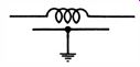
Fig. 1. Symbol
for a delay line.
A delay line for a color-TV receiver consists of a coil wound on a powdered-iron core ; its distributed capacitance is increased by enclosing the coil in a metal sheath. The symbol for a delay line is shown in Fig. 1.
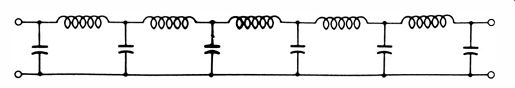
Fig. 2. Multi-section low-pass filter.
A delay line never has a completely smooth distribution of inductance and capacitance. However, a high-quality delay line is a practical approximation of this ideal. A low-pass filter (Fig. 2 ) also approximates a smooth distribution of L and C, provided a very large number of sections are used.
Such filters are employed as delay lines in lab-type scopes where as many as 30 sections may be utilized. Now, if a low-pass filter had an infinite number of sections, it would approximate a coaxial cable in effect.
Reading Between the Lines
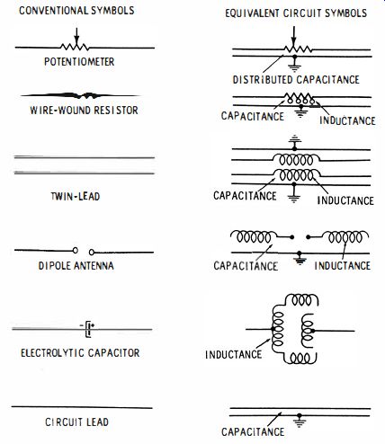
Fig. 3. Distributed parameters of components.
Distributed parameters are ordinarily not explicit, but only implied in conventional symbols, therefore you must visualize the distributed parameters. Fig. 3 shows the meaning of this requirement. An ordinary potentiometer is symbolized as a resistor with a variable arm. But, as will be demonstrated subsequently, a potentiometer often has a significant distributed capacitance that must be taken into consideration in high-frequency or square-wave operation. You must visualize the distributed capacitance as depicted in the equivalent circuit symbol for a potentiometer in Fig. 3. This representation is in accordance with the conventional representation of distributed capacitance in a delay line, as shown in Fig. 1.
It will subsequently be demonstrated that a wirewound resistor cannot be visualized as a simple resistance at video frequencies. Instead, it is necessarily considered as an RLC component; the three parameters are distributed, and an attempt to visualize the electrical picture is given in Fig. 3.
The small loops shown in the equivalent symbol for a wire-wound resistor indicate the distributed inductance-the distributed capacitance is indicated as before.
Note that the conventional symbol for twin lead denotes the presence of distributed capacitance only. As a matter of fact, resonant stubs could not exist if the twin leads lacked distributed inductance. An attempt to visualize the physical facts is shown in Fig. 3 ; the conductors are shown as long small coils, with distributed capacitance as previously explained.
An electrolytic capacitor, as you will recall, often exhibits objectionable inductance when operated at high frequencies.
Hence, in Fig. 3, this distributed inductance is represented as the electrodes of the capacitor.
Properties of Coaxial Cables
A coaxial cable clearly has distributed capacitance because the central conductor is surrounded by a metal sheath. The two metal surfaces form the "plates" of a capacitor. Although it is not obvious, a coaxial cable also has distributed inductance, since a wire has inductance, even if it is not wound into a coil.
The inductance of a straight wire is comparatively small, but it becomes an important parameter when a coaxial cable is driven at high frequencies. Note that a coaxial cable also has resistance-the wire has a DC resistance, although it may be very small. At very high frequencies skin effect causes a wire to have a considerably higher AC resistance.
The resistance of a coaxial cable cannot be neglected unless it is comparatively long. For example, stubs are evaluated on the basis of distributed capacitance and inductance only. Note that there are two forms of resistance in a coaxial cable ; the metal has a small resistance, and the dielectric has a small leakage. Since the series resistance is very low, and the shunt resistance is very high, both can be disregarded unless the cable is very long, as in a community TV system. Briefly, the series and shunt resistance in a very long cable cause the cable to respond as a low-pass filter. To extend the cut-off frequency, large-diameter conductors are used with air spacing.
TESTS OF STUBS, CABLES, AND LINES
A stub is a comparatively short length of coaxial cable or twin lead. If it is shorted at the far end, it is called a shorted stub. Conversely if it is left open at the far end, it is called an open stub. The terminals of the stub will appear as an inductance, capacitance, very high resistance, or very low resistance, depending on the applied frequency. When a stub looks like a very high resistance, it is operating as a parallel resonant circuit. When it looks like a very low resistance, it is operating as a series-resonant circuit. When it looks like a capacitance or inductance, it is operating off resonance.
Shorted Stub
The most common test of a stub is a measurement of its resonant frequency. A grid-dip meter is most convenient for the purpose. Simply hold the tank of the grid-dip meter near the end of the stub, and tune the instrument for a dip indication. A shorted stub (Fig. 4A) has an infinite number of resonant frequencies. The lowest resonant frequency corresponds to an electrical length of one-quarter wavelength. The electrical length is almost the same as the physical length for an air-spaced line. At its lowest resonant frequency, a shorted stub has the voltage and current distribution depicted in Fig. 4B.
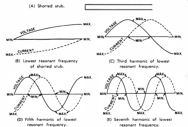
Fig. 4. Voltage and current distribution along a shorted stub.
(A) Shorted stub. (B) Lowest resonant frequency of shorted stub. (C) Third harmonic of lowest resonant frequency. (D) Fifth harmonic of lowest resonant frequency. (E) Seventh harmonic of lowest resonant frequency.
The quarter-wave stub is the equivalent of a parallel-resonant circuit, so its terminal impedance is very high. If you apply Ohm's law to the terminal voltage and current depicted in Fig. 4B, this fact becomes clear. Since R = E/I, then in this case, R = E/O, or the. input resistance is infinite, at least in theory. In practice, the stub wires have a small RF resistance, and there is a little loss from radiation, which is equivalent to RF resistance also. Hence, the terminal impedance is not infinite, although it is very high. The better is the design of the stub, the higher is its input impedance in quarter wave operation.
Because the wires are short-circuited, the voltage is zero at the shorted end of the stub. The current flow is maximum through the short-circuit. Ohm's law is written R = O/I for the shorted end, which indicates that the stub has minimum impedance at the shorted end. The actual impedance is not quite zero in practice, due to the RF resistance of the conductors and the small radiation loss. It is clear from the voltage and current distribution depicted in Fig. 5-4B that the impedance at intermediate points along the stub varies; if you tap in at a suitable point along the stub, you can obtain any impedance value from (almost) zero to infinity.
Reflection of Voltage and Current
A grid-dip meter test will show the next stub resonance at the third harmonic of the first resonant frequency. The voltage and current distribution for third-harmonic resonance is illustrated in Fig. 5-4C. As before, the input impedance is very high since the third-harmonic shorted stub is also the equivalent of a parallel-resonant circuit. The question may be asked why we find the voltage and current distributions depicted in Fig. 4B and C. The answer is that the electrical energy does not travel down the stub instantaneously ; instead, the energy flows at about the speed of light. When a voltage is applied at the terminals, the RF power travels down the wires until it reaches the short-circuited end.
Obviously, when the RF energy reaches the short-circuit, its voltage must drop to zero--a voltage drop cannot exist across zero resistance. Inasmuch as there is no load to consume power at the end of the stub, the energy must be reflected since energy cannot be destroyed-if it is not consumed (changed into some other form of energy), it must be reflected. The only way that a voltage can be reflected at a short-circuit is for it to be reflected 1800 out of phase; then, the resultant voltage at the short circuit is zero.
When the RF energy reaches the short circuit, the current encounters a zero-resistance path, so the current flows through the short circuit without loss. Again, its energy cannot be destroyed, and since there is no load to absorb the incident energy, the current must also be reflected. The only way that a current can be reflected at a short circuit is for it to be reflected in phase ; then the resultant current at the short circuit is maximum.
It will be seen that voltage and current reflections at the open end of the stub are exactly opposite to the reflections at the shorted end. Reflection must occur at the open end, because there is no load provided, and the energy cannot be destroyed. No current can flow across an open circuit, and hence the current reflection at the open end is 180 deg out of phase, which brings the current to zero. However, the voltage reflection at the open end is in phase, which brings the current to maximum.
Higher Harmonic Resonances
A grid-dip meter test will show that the shorted stub has resonances at each odd-harmonic frequency. Figs. 4D and E illustrate the voltage and current distributions for fifth- and seventh-harmonic resonances. From the foregoing discussion, it is clear that if the stub is tapped at the current minimum, the impedance at that point will be very high. If the stub is tapped at a voltage minimum, the impedance at that point will be very low. As surprising as it might seem, you can solder a short circuit across a stub at a voltage minimum, and no change occurs in stub characteristics. This is the reason that supports of the "metallic-insulator" type are often used to support stub installations, as shown in Fig. 5.
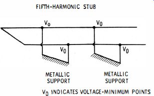
Fig. 5. Metallic insulators at minimum voltage points.
It also follows from Fig. 4A that in case the "metallic insulators" are made one-quarter wavelength in length, that they may be secured at any point along a stub or line, without causing any change in operating characteristics. In this case, the "insulators" are simply quarter-wave stubs. Of course, this method of "metallic insulation" is effective only at the correct frequency-in case of frequency drift, there will be an appreciable loss of energy.
(A) Capacitive coupling to end of stub. (B) Inductive coupling to center of stub.
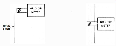
Fig. 6. Coupling to an open stub.
(A) Open stub of 300·ohm lead. (B) lowest resonant frequency of open stub. (C) Second harmonic of lowest resonant frequency.
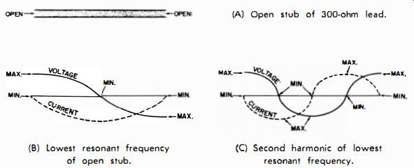
Fig. 7. Voltage and current distribution on an open stub.
Open Stubs
An open stub is a line section that is open at the far end (Fig. 7 A) . The resonant frequencies of an open stub can be measured with a grid-dip meter, as depicted in Fig. 6.
Because as the stub has infinite resistance at both ends, the voltage rises to a minimum at each end. At the lowest resonant frequency of the stub, a voltage minimum occurs at the center of the stub (Fig. 7B). The resonant frequency can be checked by capacitive coupling to one conductor, as shown in Fig. 6A. Or, inductive coupling can be used to the center of the stub, as shown in Fig. 6B. At comparatively low frequencies, it is preferable to use inductive coupling, since the dip is more pronounced. When inductive coupling is utilized, the most effective test point is at a current maximum (voltage minimum). Thus, an open stub exhibits its second resonance at the second-harmonic frequency (Fig. 7C). The current maximum then occurs one fourth of the distance from the end of the stub. An open stub has an infinite number of resonant frequencies. Note that these are all the harmonics of the lowest resonant frequency. Unlike a shorted stub, which resonates on odd harmonics only, an open stub resonates on both even and odd harmonics of the lowest resonant frequency.
INDUCTANCE AND CAPACITANCE OF CABLE OR LINE
It is difficult to measure the inductance of coaxial cable or twin lead directly, unless specialized laboratory test equipment is used. However, the inductance per foot can be determined indirectly. Recall that you can measure the capacitance of cable of twin lead with an ordinary capacitance bridge.
For example, a 6-foot length of 300-ohm twin lead measured 20 mmf of capacitance; therefore the capacitance in this example is 3.33 mmf per foot.
The characteristic impedance of the twin lead is 300 ohms, and for short lengths (which are considered lossless in practice) , Zo = VL/C. Rearranging, we have L = CZ}, or L = 90,000 x 3.33 X 10^-12 = 0.3 microhenry per foot. In this example, the rated characteristic impedance of the twin lead has been used, but if the characteristic impedance were unknown, it would have to be measured. This inductance of 0.3 micro-henry per foot is called the loop inductance. In other words, it is the inductance of both conductors in the twin lead.
CHARACTERISTIC IMPEDANCE OF CABLE OR LINE
The characteristic impedance of a cable or line is defined as the input impedance of an infinitely long sample. This is the theoretical definition, but in practice, the characteristic impedance is defined as the termination which makes the input impedance of the cable (or line ) constant, regardless of length.
For comparatively short length of cable or line, the characteristic impedance will be a pure resistance, because the short section may be considered as lossless.
A test is made most conveniently as follows: Use a line section at least five feet long, and apply the RF output from a sweep generator to one end of the line. Connect a demodulator probe and a scope across the generator-output terminals, as shown in Fig. SA. Terminate the cable with a composition resistor that has a value near the expected characteristic impedance of the line, and observe the scope pattern (Fig. SB). If the trace is not flat, change the value of the terminating resistor to obtain a flat trace. The value of the resistor is then equal to the characteristic impedance of the line section. Any VHF high-channel output from the generator is suitable in this test.
(A) Test setup. (b) Flat response.
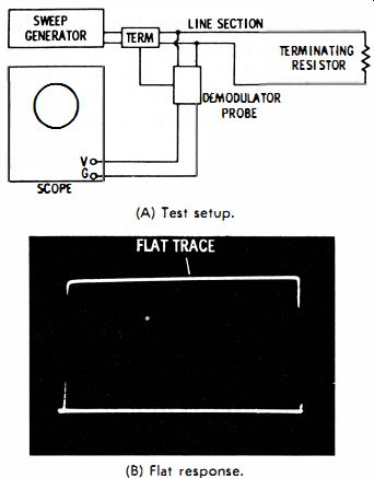
Fig. 8. Characteristic impedance measurement.
Of course, the evaluation of this test assumes that the sweep generator has a flat characteristic. In case of doubt, this should be cross-checked ; simply disconnect the line section from the test setup in Fig. 5A, and connect the terminating resistor directly across the sweep-generator output terminals. The trace should be flat if the generator is in good operating condition.
If the trace is not flat, note the curvature carefully. Then re-connect the line section to see whether this curvature is duplicated. Choose a terminating resistance that provides duplication of the reference curvature.
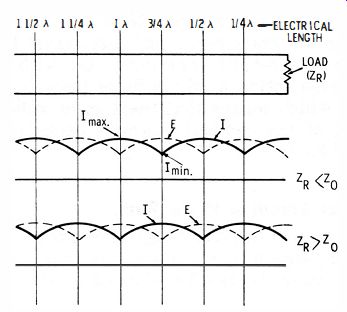
Fig. 9. Standing waves on a resistively terminated load.
STANDING-WAVE RATIO ON A LINE
An open or shorted stub has an infinite standing-wave ratio, at least in theory. With reference to Fig. 7, the voltage distribution passes through maxima and minima. In the ideal situation, the minimum voltage is zero, and Vmtlx/Vmlll = 00. Now, suppose that a line is terminated in a resistance that is less in value than the characteristic impedance (Zo) of the line.
Reflection is incomplete, because some of the electrical energy is converted into heat by the terminating resistor. Hence, the resultant of incident and reflected waves produces a voltage minimum that is greater than zero, as depicted in Fig. 9.
Suppose again that the line is terminated in a resistance that is greater in value than the characteristic impedance of the line. As before, reflection is incomplete, due to conversion of some of the electrical energy into heat. The resultant of incident and reflected waves produces a voltage minimum that is greater than zero (Fig. 9) . The ratio of Vlllux/Vmill is called the standing-wave ratio, or the voltage standing-wave ratio (VSWR). It is equal to Zo/Zn, or Zn/Zo, whichever the case may be.
If Zn = Zo, there is no reflected voltage or current at the termination. All of the incident power is absorbed by the terminating resistor and converted into heat. The reason for this matched condition is not entirely obvious. The electrical meaning of a matched load is given in Fig. 10. Consider a theoretical one-ended line of infinite length. If a battery voltage is switched into the line, a steady current is drawn ; theoretically this constant current will flow forever, because the line is infinitely long. The line can never be charged up, and no reflected energy can exist.
(A) Infinite line has no reflected energy. (b) Matched load can reflect no energy.
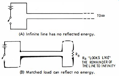
Fig. 10. Theoretical presentation of a matched load.
What is the characteristic impedance (resistance) of the infinite line (Fig. 10A) ? It is, of course, Ell as defined by Ohm's law. It has some value which is determined physically by the diameter of the conductors and their spacing. For example, Ell might equal 300 ohms. Now, let the infinitely long line be cut at an arbitrary point, and terminated by a 300-ohm resistor (Ro in Fig. 10B) . The finite line with the matched load has the same action as the infinite line-it provides the same demand, which means that there is no reflected voltage or current. All of the incident power is necessarily absorbed by the matched load.
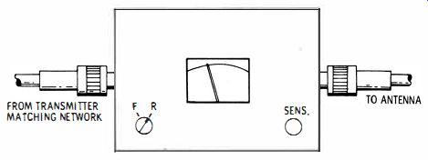
Fig. 11. SWR meter connected in a transmission line.
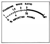
Fig. 12. Dial scale of SWR/reflected power meter.
Measurement of Standing-Wave Ratio
When a line is used to drive an antenna from a transmitter, it is desirable to obtain maximum power transfer. The maximum power transfer occurs when the characteristic impedance of the line matches the impedance of the antenna. Under this condition, there is no reflected power on the line, or, the VSWR is 1. Hence, measurements of VSWR are used as an indication of efficiency. Several methods of testing a line for VSWR are available, the most accurate of which are time- consuming. For practical purposes, a direct-reading, standing-wave-ratio meter is adequate.
An SWR meter is connected in series with the high-frequency transmission line, as depicted in Fig. 11. The characteristic impedance of the meter must match the line--50 ohms and 75 ohms are widely used impedances. If a meter is to be used with a line of different impedance, impedance transformers are required at input and output, or if a single-ended meter is to be used in a double-ended line, balun coils must be connected at both input and output.
To make a VSWR test, the function switch of the meter is first set to its forward position, and the sensitivity control is turned to obtain full-scale deflection ("Set" calibration mark in Fig. 12 ). Next, the function switch is turned to the reflected power position. The pointer then indicates the VSWR and the percentage of reflected power. Note that an appreciable amount of power is required to provide full-scale deflection ; hence, an SWR meter cannot be used with transmitters that have very low power. The lower is the operating frequency, the higher is the power level required to obtain full-scale deflection.
The schematic of a typical standing-wave-ratio meter is shown in Fig. 13. It is essentially a section of coaxial line, to which two parallel wires are coupled. Both inductive and capacitive coupling is provided by the wire. Each wire is terminated by a suitable resistance, and the terminated ends are opposed. Diode rectifiers are connected near the unterminated ends of the coupling wires. Forward power flow produces output from one diode, and reflected power flow produces output from the other diode.
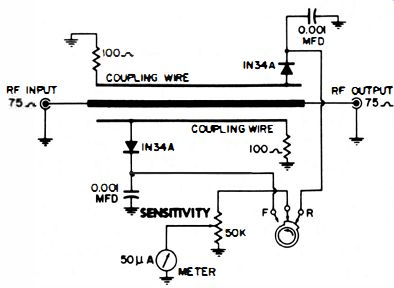
Fig. 13. Circuit of typical SWR/reflected-power meter.
Balun Configuration
Tests in which a coaxial cable is required to drive a twin lead line (or vice versa) require the use of a balun to convert a single-ended output to a double-ended output or vice versa. The construction of a simple balun is depicted in Fig. 5-14A. The balun should be at least a quarter-wavelength long at the operating frequency, although it may be longer. The balun illustrated is suitable for matching a 75-ohm, single-ended output to a 300-ohm, double-ended line. The spacing between the 150-ohm line sections should be appreciably greater than the spacing of the conductors in the line section itself.
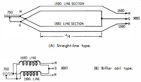
Fig. 14. Typical balun matching couplers.
(A) Straight line type. (B) Bifilar coil type.
The line sections can also be wound into loose coils, as illustrated in Fig. 14B. The spacing between turns should be greater than the spacing between the conductors of the line sections. This provides a more compact construction. Note that a balun can make only a 4/1 impedance transformation.
The exact values of the input and output impedances can be varied by choosing suitable characteristic impedances for the line sections-however, the input/output impedance ratio is always 1/4 or 4/1. The balun can be tested for proper operation as shown in Fig. 15.
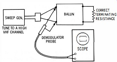
Fig. 15. Efficient balun shows flat trace.
Stub Matching Any two impedances can be matched by means of resonant stubs. The most convenient method employs a single, series, quarter-wave section as shown in Fig. 16. Suppose you wish to match a 50-ohm line (or cable ) to a 250-ohm line (or cable ).
QUARTER-WAVE SECTION
(A) Twin-lead impedance transformer. (b) Coaxial impedance transformer.
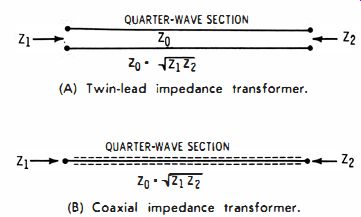
Fig. 16. Impedance matching with resonant stubs.
The quarter-wave section must then have a characteristic impedance equal to \150 x 250, or 11 1.8 ohms. The only difficulty you will encounter is obtaining line or cable having the desired characteristic impedance. It is often necessary to construct the desired quarter-wave section experimentally and to verify its characteristic impedance with a sweep generator and scope by the method depicted in Fig. 18.
Demodulator Probes
Two different types of demodulator probes are used to test components having distributed parameters. Single-ended components such as coaxial stubs are tested with a single-ended probe (Fig. 17 A). Double-ended components such as twin-lead stubs are tested with a double-ended probe. As shown in Fig. 17B. If you attempt to use a single-ended probe to test a balanced stub or line, the display is likely to be erroneous due to upset of the balanced current flow in the two conductors.
(A) Single end. (b) Double end.
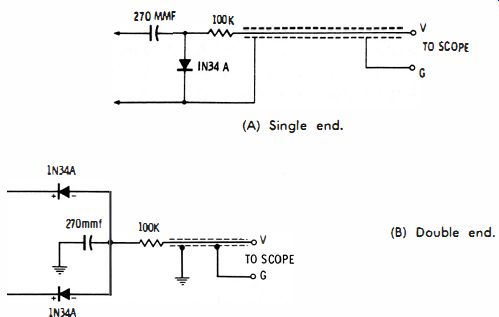
Fig. 17. Demodulator probe.
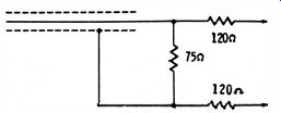
Fig. 18. Simple resistive balun.
Sweep-Generator Output Termination
Most sweep generators have a single-ended output cable.
This arrangement is used directly to drive a single-ended component. However, if the generator is used to drive a double-ended component, its single-ended output should be converted to double-ended output. This can be done most effectively by means of a balun (Fig. 14B ). However, a simpler though less efficient resistive balun can be used, as shown in Fig. 18.
TEST OF DELAY LINE
Delay lines in color-TV receivers are usually tested initially by displaying the frequency-response curve of the Y-amplifier.
A video-frequency sweep generator, demodulator probe, and scope are used, as shown in Fig. 19. A typical response curve is seen in Fig. 20. The curve shape should be checked against the receiver service data specification. If substantial distortion is present, and the delay line is suspected, disconnect the line and check it out with an ohmmeter. The winding might be open or leaking to ground.
Because the inductance and capacitance in a delay line does not have a completely smooth distribution, the line develops minor resonance at various frequencies. Hence, the contour of a Y -amplifier curve is not smooth but instead displays undulations as shown in Fig. 20. This characteristic is normal for delay lines used in TV receivers.
TESTING WI REWOUND RESISTORS FOR REACTANCE
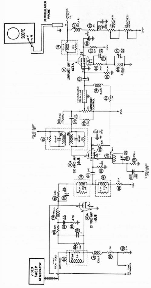
Fig. 19. Test method for delay line.
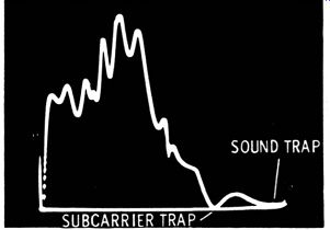
Fig. 20. Typical response curve of delay line test.
(A) Test setup for measurement. (b) Equivalent circuit of resistor.
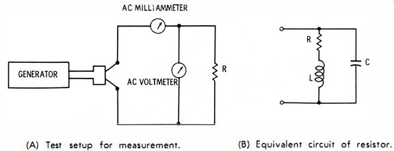
Fig. 21. Measuring reactance of a wirewound resistor.
(A) Conventional schematic symbol fo a potentiometer. (B) Schematic of equivalent distributed capacitance.
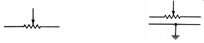
Fig. 22. Distributed capacitance in a potentiometer.
A wirewound resistor is a coil of resistance wire; hence it has inductance and distributed capacitance. As the operating frequency is increased, the impedance of most wirewound resistors exceeds the resistance value measured on an ohm-meter. An impedance measurement is made as shown in Fig. 21. The impedance is given by Ohm's Law : Z = Ell. Ordinary wirewound resistors will show a small increase in impedance at 1 mhz, compared with their DC resistance. As the test frequency is increased to several megacycles, the impedance usually increases substantially. For example, a 50 watt, wirewound resistor with a DC resistance of 1,000 ohms measured an impedance of 1,600 ohms at 5 mhz.
DISTRIBUTED CAPACITANCE OF POTENTIOMETER
In theory, a potentiometer consists of resistance only, but in practice its distributed capacitance (Fig. 22 ) must be taken into account. The higher the resistance value, the more significant is the effect of the distributed capacitance. For example, a vernier attenuator in a 4- mhz scope might be a 2K potentiometer. The vernier attenuator imposes negligible distortion on complex waveforms, regardless of the attenuator setting. On the other hand, if a 5K potentiometer were used as a vernier attenuator in a 4-mhz scope, serious distortion of complex waveforms would be observed at various settings of the potentiometer.
(A) Setup for square-wave test. (B) Spikes indicate high C,,/R ratio.
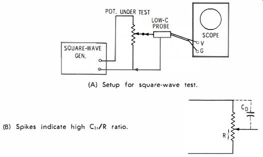
Fig. 23. Square wave test of a potentiometer.
Test of Potentiometer
A practical test of a potentiometer for distributed-capacitance effects can be made by applying a square-wave voltage as depicted in Fig. 23. Increase the square-wave frequency in steps, and observe the square-wave reproduction. Note that when the potentiometer is "wide-open," no distortion will be observed in the square-wave pattern, regardless of the test frequency. On the other hand, at some upper square-wave frequency, distortion appears when the potentiometer is set below its maximum position-the distortion changes as the pot is set to lower output.
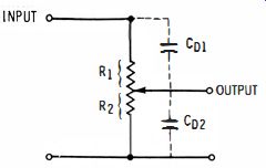
Fig. 24. Output is undistorted when R,Co, = R,C""
Distortion of Test Waveform
At some settings of the pot, you will observe differentiation of the square wave, and at other settings integration occurs.
Often you will be able to find one critical setting of the pot at which the differentiation cancels out the integration, and the output square wave is undistorted. At this critical setting, depicted in Fig. 24, the time constants of the two potentiometer sections happen to be equal.
Obviously, a potentiometer should not be used in a given application if it shows distortion at any setting. A pot with a lower resistance must be selected, in which the distributed capacitance has negligible effect over the frequency range required. The output capacitance of the potentiometer circuit is also a factor of importance. For example, in Fig. 23, a low capacitance probe is used in the test. If the probe should have 10-mmf input capacitance, this is the output capacitance load on the potentiometer. If the test were made with a direct cable to the scope, the output capacitance load might be increased to 100 mmf, reducing the frequency capability of the pot. Hence, the section of potentiometer resistance must be made with respect to the output capacitance in the circuit application, as well as the distributed capacitance of the pot.