AMAZON multi-meters discounts AMAZON oscilloscope discounts
As the term indicates, wave shaping techniques are concerned with changing one waveform into another. Television receivers and transmitters, radar equipment, industrial-electronic control devices, and electronic computers are examples of the application of these techniques. You will find an extensive array of circuit actions employed in waveshaping processes. Differentiation, integration, clipping, clamping, resonance, rectification, timing, mixing, counting, amplifying, and heterodyning are all used. These circuit actions are not covered in detail in these pages, but interested readers may refer to specialized texts such as the Basic Electronics series.
WAVESHAPING WITH RESONANT CIRCUITS
Fig. 4-1 illustrates how a tuned circuit shapes a complex waveform into a sine wave. If you apply each of the waveforms of Fig. 4-1A individually to the tuned transformer (Fig. 4-1B) , the secondary output is a sine wave in each case. Maximum output amplitude is obtained when the wave shaping circuit is resonant to the fundamental frequency of the input waveform. However, a sine-wave output of less amplitude results when the circuit is tuned to any odd harmonic of the input waveform. A small sine-wave output is also obtained by tuning to the ringing frequency of waveform 4 in Fig. 4-1A.
(A) Input waveforms. (B) Circuit and output waveform.
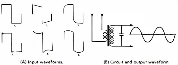
Fig. 4-1 . Waveshaping with resonant circuit.
In passing it is instructive to note the chief characteristics of these input waveforms. Thus, 1 depicts an ideal square wave. The tilt along the top and bottom of 2 results from phase shift of the harmonics in the reference square wave-in other words, all the harmonic voltages in 2 have the same amplitudes as in 1. Diagonal corner rounding in 3 is the result of high frequency attenuation and phase shift. The overshoot and ringing in 4 is caused by LC elements in the source, such as inadequately damped peaking coils in a video amplifier. Curvature in the top and bottom of waveform 5 is the result of low-frequency attenuation-the small amount of tilt results from harmonic phase shift. The opposite curvature displayed in 6 is the result of high-frequency attenuation with negligible phase shifts.
The tuned secondary circuit in Fig. 4-1B must have a high Q to provide an un distorted sine-wave output. Therefore, its frequency response is sharp, so that only one frequency is transferred from primary to secondary. The symbol Q refers to the quality factor of the resonant circuit; Q = XdR in most practical situations. XL is the number of inductive ohms at the resonant frequency of operation, and R is the AC resistance of the coil. The effect of the capacitor on Q value is commonly neglected, because nearly all the circuit losses are imposed by the inductor.
A generalized configuration is depicted in Fig. 4-1, but you will probably be interested in a specific application also. Refer to Fig. 4-2; here a quartz crystal is used to develop a 3.58-mhz CW signal from a complete color signal in a color-TV receiver.
The complete color signal contains 3.58-mhz bursts which follow each horizontal-sync pulse. Thus, the 3.58-mhz signal has an interrupted and recurrent characteristic. It is desired to shape this succession of bursts into a continuous sine wave.
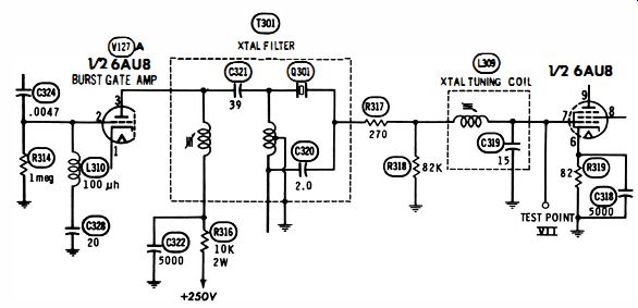
Fig. 4-2. Application of ringing circuit in color-TV receiver.
The required waveshaping action is obtained through the use of a quartz crystal as a resonant circuit having a very high Q. It is called a filter, because it separates, or filters out, the 3.58 mhz burst frequency from any other frequencies which might be present. An adjustable coil is provided in series with the crystal so that its resonant frequency can be adjusted exactly to that of the burst. In addition, correct adjustment of the slug provides an output phase which is exactly the same as the transmitted burst phase.
Although the input to the crystal filter is an interrupted series of bursts, the output is essentially a continuous sine wave. This characteristic results from the very high Q of the crystal.
It can be shown that when Q is high, a large energy storage takes place-between the incoming bursts, output is sustained by this large reservoir of stored energy in the crystal. The con
figuration is also called a crystal-ringing circuit. When an in coming burst energizes the crystal, it vibrates much as a bell does when it is struck. Of course, this mechanical vibration is very rapid; it occurs 3,580,000 times a second.
SCOPE FREQUENCY RESPONSE
Since a color burst has a 3.58-mc frequency, it cannot be viewed with a scope unless wide-band response is provided.
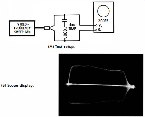
Fig. 4-3. Frequency response of scope vertical amplifier. (A) Test setup.
(B) Scope display.
Scopes used to check waveshapers such as shown in Fig. 4-2 should have a reasonably uniform response out to 4 mhz. Note in passing that you can easily check the frequency response of a scope with a video-frequency sweep generator, as shown in Fig. 4-3A. This is an FM generator which provides an output varying periodically from about 100 khz to 5 mhz.
Note also the 4-mhz series-resonant trap in Fig. 4-3A. As the FM voltage sweeps through the 4-mc point, the trap absorbs a small amount of energy from the circuit and produces a dip in the wave envelope near the right end. This is called an absorption marker and is itself a waveshaping operation from one point of view. Its specific purpose, however, is to identify accurately the 4-mhz point on the envelope of the waveform.
TIME MARKERS FROM RINGING CIRCUIT
Ringing-circuit waveshapers are also found in laboratory equipment and radar indicators. However, the purpose of wave shaping is somewhat different in these instances. For example, it has been previously mentioned that instantaneous voltages on a waveform can be marked by intensity-modulating a scope from a voltage of known frequency. This is basically a time-marker technique. This technique is used in radar equipment for range estimation and measurement. A dominant characteristic of such waveshapers is synchronization with the displayed signal.
A resonant circuit contained in a shock-excited oscillator configuration provides generation of the desired marking frequency plus synchronization with the signal repetition rate.
A circuit in which the plate current of a switching tube flows through the inductor of a tank circuit is commonly used to produce a damped train of oscillations which is initiated by tube cutoff. A typical system is illustrated in Fig. 4-4. A negative-going square pulse drives the grid of V1 below cut-off at the instant that the sweep starts, thus causing L1 and C2 to ring. Sharp, well defined marker pulses are produced by feeding the output from the tank circuit through the remaining circuitry shown in Fig. 4-4.
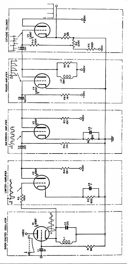
Fig. 4-4. Waveshaper for producing timing pulses synchronized with drive signal.
The damped wave trains are clipped and amplified by V2 so that its plate output is an approximation to a square wave.
Resistor R2, in series with the grid, limits the grid current so that the ringing circuit remains lightly loaded. This prevents the damped sine wave from decaying too rapidly for proper utilization. The cathode bias developed across R3 and C3 prevents the grid from going extremely positive, which also assists in minimizing grid-current flow. A low plate voltage is used to provide good clipping action. The output from V2 is coupled to the grid of V3, which is an overdriven amplifier and produces a good approximation to a square wave at its plate.
The peaker-amplifier tube (V4) has as its plate load inductor (L2) shunted by resistor R9. This inductor resonates with its distributed capacitance at a frequency of approximately 2 mhz. When the tube is cut off by the negative-going square wave, the coil is shock-excited into oscillation. However, the shunt resistance damps the oscillation almost completely before one cycle is completed so that a positive pulse of approximately 0.25 microsecond duration is produced. When the grid swings positive, a negative pulse of smaller amplitude appears at the plate. This negative pulse has no significance, since the following tube is biased below cutoff so that only positive pulses can produce an output.
Note that the grid of V4 is returned to a positive potential, rather than to ground, in order to insure high conduction in the tube just before the grid swings negative. The large resistor (R8) in the grid circuit limits the grid current to a low value. From the pulse generator the shaped waveform is fed to a cathode follower which is biased below cutoff. By adjusting this bias so that the positive peaks raise the grid above cutoff by the desired amount, the amplitude of the marker pulse can be controlled. Thus, the end result of the waveshaping process is to generate a series of sharp and accurately timed pulses which are always locked in with the repetition rate of the deflection voltage.
WAVESHAPING WITH RC CIRCUITRY
It is apparent that RC circuits can be used for a wide variety of waveshaping functions. For example, an RC configuration can be used to change a peaked-sawtooth wave into a pulse type wave. This method is commonly used to produce a vertical-retrace blanking pulse in TV-receiver circuitry. The peaked sawtooth is unsuitable for blanking, inasmuch as it would cause severe picture shading from top to bottom of the screen. On the other hand, the pulse-type waveform has an essentially flat top which causes negligible picture shading.
Differentiating and integrating circuits only produce approximations to mathematical differentials and integrals. If the resistance is very small, the circuit action is more nearly in accord with the mathematical ideal. In theory the result of differentiating a true square wave is to produce a series of pulses that are infinitesimal in width and infinite in amplitude. The ideal situation is approached if you utilize a very small series resistance-the voltage drop across the resistor becomes a very narrow pulse. Again, in theory the result of integrating these pulses is to form a square wave; the first suddenly charges the capacitor to a certain voltage which is held until the next pulse arrives. This next pulse has an opposite polarity which suddenly brings the capacitor voltage once more to zero-thus a square wave is formed. It can be seen that differentiation and integration are opposite operations.
(A) Circuit. (B) Waveform with small capacitance. (C) Waveform with large capacitance.
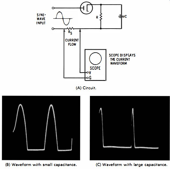
Fig. 4-5. Current waveform. in a half-wave rectifier with RC load.
The waveforms in Fig. 4-5 result from application of a sine-wave voltage to a circuit containing nonlinear resistance such as a rectifier. When the load contains capacitance, as in Fig. 4-5, the diode is back-biased, and current flow occupies less than a half cycle. Since a complete cycle occupies 360°, a half cycle occupies 180°, and the current waveforms in Fig. 4-5 occupy a progressively smaller number of degrees. Accordingly, such waveforms are described in terms of their conduction angle.
Capacitor C charges in proportion to the time-constant of the load and places a positive bias on the cathode of the diode.
The higher the bias voltage, the smaller is the conduction angle.
This bias consists of a DC component and an AC component.
The DC component can be measured with a DC voltmeter or with a DC scope. Superimposed on this DC component is the AC ripple voltage (Fig. 4-6) . The ripple waveform in this circuit is a semi sawtooth. It rises to a peak with the current peak; the diode is then cut off by back bias, and the capacitor charge decays through R to form the semi-sawtooth wave.
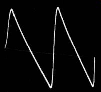
Fig. 4-6. Ripple-voltage waveform in half-wave rectifier with RC load.
Note in Fig. 4-5 that the current waveforms are both shown at the same amplitude. This is done because the conduction angle is being emphasized. However, as the conduction angle is decreased, the amplitude of the current waveform becomes less.
In turn, the amplitude of the voltage waveform becomes lower as the value of C is increased. This is simply another way of saying that the amplitude of the ripple voltage decreases when you make the filter capacitor larger. If the filter capacitance or resistance R were infinite, the time constant would also be infinite and the ripple voltage would be zero. Likewise, the current-conduction angle in Fig. 4-5 would be zero, and the amplitude of the current waveform would be zero.
If you utilize a dual-trace scope, both the current waveform and the voltage waveform can be displayed simultaneously on the screen. Or, if you use an electronic switch, both current and voltage waveforms can be displayed simultaneously on the screen of an ordinary scope. Dual-trace presentation is very useful during circuit development, because the overall result of a circuit change can be observed without making connection changes or employing more than one scope. Dual-trace patterns are also advantageous in certain circumstances because the phase relation between any two chosen waveforms is displayed on the screen.
Note that a single-trace display does not show the relative phase of a waveform unless external sync is used. This lack of phase information on the internal-sync function results from the lack of a reference trigger or sync voltage. On the other hand, when external sync is used, the sawtooth oscillator in the scope is triggered independently of the waveform which is passing through the vertical amplifier. Likewise, when an electronic switch is used, the two waveforms are alternately sampled so that phase information is presented.
WAVESHAPING BY NON-LINEAR RESISTANCE
The varying conduction angles illustrated in Fig. 4-5 result from the time constant of the RC load circuit. In addition, the rectifier is an essential component in the waveshaping circuit.
A rectifier is a special case of nonlinear resistance--it is a form of resistance in which current will flow in one direction only; current flow is blocked in the reverse direction. Other forms of nonlinear resistance used in waveshaping circuits conduct current in either direction, but the current flow is disproportional to voltage. In other words, the resistance value depends on the instantaneous current value.
A practical example of waveshaping makes use of the non-linear resistance characteristic inherent in a semiconductor diode. The resistance of a diode varies with current; it is basically a logarithmic relation, and the exact characteristic can be controlled by employing a suitable value of fixed resistance in the circuit. Two semiconductor diodes can be connected in opposite shunt polarity, so that a symmetrical wave shaping action is obtained on both positive and negative half cycles of the signal.
Logarithmic waveshapers are used because the output from the waveshaper can be made proportional to decibels--you will recall that db are a logarithmic unit of output. Inasmuch as ear response is proportional to decibels (rather than volts or watts) , it is clearly advantageous to use a db waveshaper when analyzing audio signals. Then, the deflection on the scope screen is directly proportional to audibility. Eye response is also proportional to db; hence, engineers sometimes evaluate receiver response curves with the aid of a logarithmic waveshaper. The height at any point on the response curve is then proportional to the effective contrast of the picture which will be reproduced.
The effect of logarithmic waveshaping on a sine wave is to compress the peaks of the waveform. The output from a logarithmic waveshaper at first rises almost as fast as the input signal ; then, the output becomes less as the input signal continues to rise. At high input amplitude, the output increases very slowly. In theory, the input voltage would have to be infinite to completely level off the output; however, in practice the dynamic range of the tubes and semiconductor diodes restricts the db range which you can accommodate with a logarithmic waveshaper.
LINEARIZING WAVESHAPERS
Just as a controlled nonlinear output is desired in some waveshaping arrangements, you will find many applications in which a waveshaper is used to linearize a curved waveform.
A common example is the linearization of a sawtooth waveform which is distorted in that the rising portion is concave or convex. The fundamental response of an RC circuit is exponential. The most common problem is to shape an exponential curve into a linear trace. When a capacitor is charged through a series resistor, a semi-sawtooth voltage waveform is produced across the capacitor. To improve the sawtooth linearity, various auxiliary wave shaping circuits may be employed.
The choice in a particular application is based on considerations of economy, reliability, and accommodation to normal tolerances. For example, if the waveshaping network contains a tube, potentiometers must often be used in place of fixed resistors to compensate for tolerances on replacement tubes. A potentiometer is much more expensive than a fixed resistor, but it is the most economical solution to the problem.
Compensating controls in waveshaping networks can often be eliminated by utilizing a large amount of negative feedback.
However, the output voltage is greatly reduced, and added amplification is required to bring up the output level. This is a comparatively costly solution. The sawtooth linearity can be improved by utilizing a high value of source voltage to charge the capacitor-only the initial portion of the exponential is then passed into the output circuit (Fig. 4-7) . This reduces the curvature in the waveform. Note that with the 10-volt battery, the excursion from 0 to 6 volts on the A curve is considerably nonlinear. If a 20-volt battery is used, you will obtain 6 volts output at the 30% point on the curve, and the excursion from 0 to 6 volts is then fairly linear.
If the charging voltage is indefinitely increased, the sawtooth rise can be made as nearly linear as desired. However, this is not always the most economical solution, because the cost of high-voltage power supplies and the associated component parts is often excessive compared with other means of corrective waveshaping. You can use a comparatively low supply voltage and still obtain an essentially linear rise if you replace the charging resistor with a pentode vacuum tube-a pentode is a good approximation to a constant-current device. But a tube is so much more expensive than a resistor or potentiometer that other approaches will generally be preferred.
Compensatory Distortion
In many cases the initial waveshaper will be supplemented by a network or device which introduces a compensating distortion. An example is depicted in Fig. 4-8. Here, R and C form an integrating network which shapes the square wave into a semi-pyramid wave. The rising and falling portions are curved.
The integrator is followed by the RC divider network R1C1, R2C2. When C1 is adjusted so that the time constant R1C1 equals the time constant R2C2, no compensating distortion is introduced-the output waveform is simply attenuated. However, if C1 is decreased, the output waveform can be linearized, as shown for the compensated case. If C1 is further decreased, the curvature of the input waveform is reversed, due to over compensation.
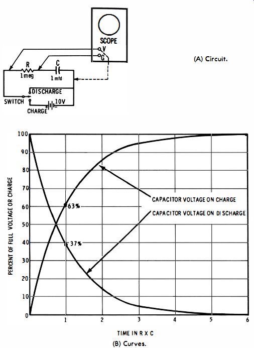
Fig. 4-7. Capacitor charging and discharging. (A) Circuit. (B) Curves.
The required value of C1 for correct compensation depends on the repetition rate of the square-wave generator. If the operating frequency is changed, C1 must be readjusted. The values of R1 and R2 should be comparatively high-1 or 2 meg-ohms are generally suitable values. If R1 is equal to R2, the attenuation of the compensating network will be about 50%.
The value of C2 should be chosen to give a suitable control range, but C2 is always considerably smaller than C. The value of R is selected to give a fair approximation to a pyramid wave so that excessive compensation will not be required. It is evident that the impedance of the integrator is much lower than the impedance of the compensating network.
(A) Circuit. (B) Output waveforms.
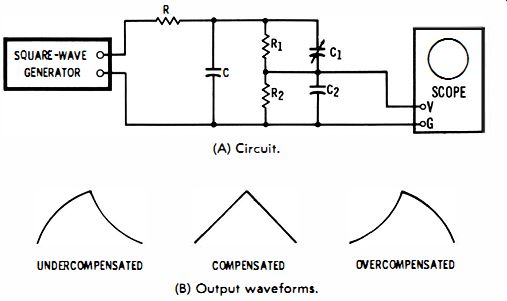
Fig. 4-8. Example of compensatory distortion.
Since the output impedance of the compensating network is comparatively high, it will not function properly with heavy loading. A scope has high impedance; hence, it does not load the circuit objectionably. Likewise, you can drive any amplifier with high input impedance without upsetting the compensating network. Note that this compensating network is basically the same configuration as used in a step attenuator for a scope. The difference is that a compensating network is adjusted to introduce a controlled amount of distortion, while the step attenuator in a scope is adjusted for distortion less output.
Compensating Tube Characteristic
When an amplifier follows the waveshaper, it is economical to introduce the compensating distortion by operating the amplifier tube on a nonlinear portion of its characteristic. Thereby, the attenuation inherent in the voltage-divider configuration of Fig. 4-8 is avoided. Note the sawtooth waveform shown in Fig. 4-9.
The wave shape can be linearized in the subsequent amplifier stage, as shown in Fig. 4-10. The tube is operated in class AB by suitable adjustment of cathode bias, with the result that the transfer characteristic is curved. This curvature compensates for the curvature of the input waveform so that the amplifier produces a linear sawtooth output (Fig. 4-10B) . It is evident that the gain of the amplifier is reduced when the cathode bias is increased (curvature of the transfer characteristic increased) , so that the linearity control incidentally affects the output amplitude. Adjustment must be made at another point in the system to compensate for this.
Fig. 4-9. Nonlinear sawtooth waveform.
WAVESHAPPING FOR IMPEDANCE LOAD
The sawtooth waveform depicted in Fig. 4-10 is suitable only for driving a sawtooth current through a resistive load (Fig. 4-11A). When a sawtooth voltage is applied across an inductance, the current waveform is not a sawtooth. To obtain a sawtooth current through an inductance, a rectangular type of voltage waveform must be applied (Fig. 4-11B) . In the case of the horizontal-deflection coils in a yoke, the load can be considered as practically a pure inductance; hence, a rectangular voltage is applied to the horizontal-deflection coils. As a result, a sawtooth current flows and generates a sawtooth variation of the magnetic field. The beam is deflected horizontally in the cathode-ray tube by this varying magnetic field.
The vertical deflection coils in a yoke contain both inductance and resistance. Hence, neither a sawtooth voltage nor a rectangular voltage across the vertical coils can produce a sawtooth current How. Instead, the driving voltage must consist of a sawtooth wave plus a rectangular wave. When you add saw-tooth and rectangular waveforms, the sum is a peaked-sawtooth waveform (Fig. 4-11C). The sawtooth component produces a sawtooth current flow through the resistance of the coils, while the square component produces a sawtooth current through the inductance of the coils. The total current flow through the coils is accordingly a sawtooth waveform.
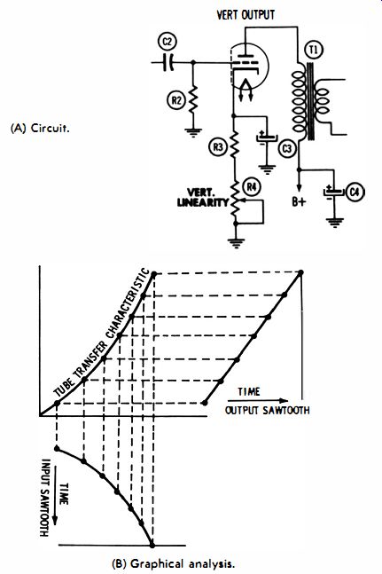
Fig. 4-10. Effect of compensating tube characteristic in a TV-receiver deflection
circuit. (A) Circuit. (B) Graphical analysis.
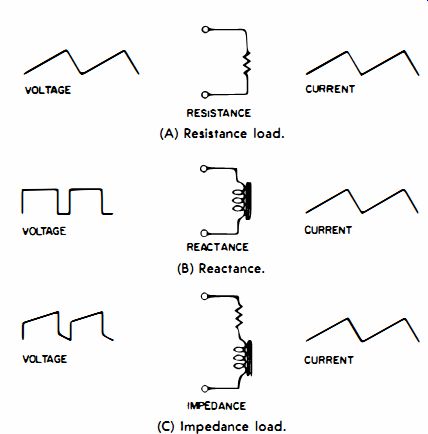
Fig. 4-11. Voltage waveforms needed to produce a sawtooth current. (A) Resistance
load. (B) Reactance. (C) Impedance load.
Peaked-Sawtooth Waveshaper
To produce a peaked-sawtooth voltage wave, a peaking resistor is connected in series with the sawtooth capacitor, as shown in Fig. 4-12. Here is how it works: suppose that the sawtooth capacitor C1 is charged to the positive peak of the output waveform. The tube then conducts briefly (for the flyback interval) , and during conduction the plate is practically shorted to ground, because the plate resistance falls to a very low value when the tube conducts heavily. Accordingly, the sawtooth capacitor discharges quickly. However, C1 is unable to fully discharge during the rapid Flyback interval, because R2 restricts the electron flow.
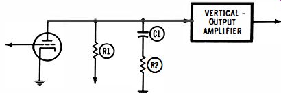
Fig. 4-12. Circuit for producing a peaked-sawtooth waveform.
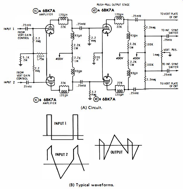
Fig. 4-13. Differential mixer. (A) Circuit. (B) Typical waveforms.
The tube is cut off following the flyback interval, leaving the residual charge on C1, which appears in the output waveform as the peaking pulse. The B+ voltage then recharges C1 through R1 and R2. This produces the sloping portion of the peaked sawtooth waveform. The value of R2 depends on the ratio of inductance to resistance in the vertical deflection coils.
The larger the L/R ratio, the larger is the peaking pulse required, and in turn the greater is the resistance required for R2.
DIFFERENTIAL MIXER
The differential mixer is a waveshaping configuration commonly used in laboratory-type oscilloscopes. Such scopes are said to have push-pull input, differential input, or double ended input. A typical configuration is shown in Fig. 4-13. It is--basically a push-pull amplifier which drives the vertical deflection plates in a cathode-ray tube. It is evident that if a positive voltage is applied to V1A, the CRT beam will be deflected in an opposite direction than if a positive voltage is applied to V1B. Suppose that equal positive voltages are applied from each gain control. The two voltages balance out in the amplifier, and no beam deflection occurs. Otherwise stated, input voltages of the same polarity subtract. On the other hand, input voltages of opposite polarity add. Thus, if you apply I positive volt to V1A, for example, the beam might be deflected upward 1 inch.
If at the same time you apply 1 negative volt to V1B, the beam will be deflected upward 2 inches. Next, suppose you apply 1 negative volt to V1A; the beam will be deflected downward 1 inch. If you then apply 1 positive volt to V1B, the beam will be deflected downward 2 inches.
It is evident that the differential mixer is basically an analog computer arrangement which produces the difference between two input signal voltages. In order to do so, the two gain controls must be identical; this follows from the requirement that two equal input voltages of the same polarity must produce an output of zero. The input system is actually a three-terminal arrangement, because there are two input channels and a ground reference. However, unless you encounter circulating ground currents, you can neglect the ground reference. In other words, either Input 1 or Input 2 can be used as a conventional ground lead in single-ended operation. For double-ended operation, Inputs 1 and 2 are applied at two "hot" points in the circuit under test.
An example of double-ended operation is the display of the voltage waveform across a coupling capacitor. Both ends of a coupling capacitor are hot. In many cases, the signal voltage is the same at both ends of a coupling capacitor, and in this situation there will be no vertical deflection on the scope screen.
But if a coupling capacitor has a comparatively small value, there is a different signal voltage at each end of the capacitor, and the difference between them is the voltage across the capacitor. A double-ended scope displays this difference signal.
In sync circuitry, for example, a coupling capacitor may be connected between two active circuits, each of which generates a different waveform. The waveform found at each end of the capacitor is quite different. An illustrative example is depicted in Fig. 4-13B. Note how the output waveform is the difference between the two input waveforms. The output waveform is displayed on the scope screen. It shows the voltage drop across the coupling capacitor.
Another practical example of differential mixing concerns the suppression of common-mode hum. When a scope has long input leads, such as half a mile to a missile-launching site, a single-ended monitor scope may display so much hum voltage that the pattern is useless. However, if a push-pull signal is utilized and fed into a differential-input scope, the hum voltage does not appear on the screen. The reason is that the input leads pick up hum voltage in the same phase-accordingly, the hum voltages on the input leads cancel out. On the other hand, the desired signal flows in the leads with opposite phases, so that the push-pull signals add in producing the scope-deflection voltage.
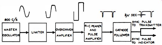
Fig. 4-14. Block diag. timer.
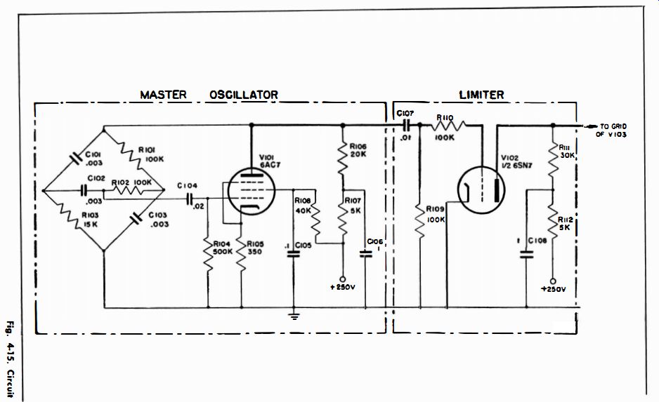
Fig. 4-15
WAVESHAPERS IN RADAR TIMERS
A radar timer establishes the pulse-repetition rate of the system and synchronizes the response of the other components.
The most obvious synchronizing action is that of causing the CRT deflection to start at the same instant that a pulse of RF energy is radiated. The block diagram shown in Fig. 4-14 shows the method used in the timer to produce the trigger pulse.
The master oscillator in this system generates an 800-cycle sine-wave voltage. The sine wave is passed through a limiter stage to produce a waveshape which is approximately square.
An overdriven amplifier is utilized to make the sides of the square wave more nearly vertical. In this way a sharp pulse of approximately 2 microseconds duration with a well-defined leading edge can be derived from the RC peaker which follows the overdriven amplifier. The positive pulse of the peaker output is selected and amplified. This pulse is used to trigger the transmitter and to synchronize the start of the CRT deflection.
A circuit diagram of the timer is shown in Fig. 4-15. The circuit employed to control the repetition rate is a phase-shift oscillator. Its output is a sine wave having good frequency stability that produces a trace free from jitter.
Master Oscillator
Oscillation is obtained by coupling the plate of V101 back to the grid through an RC bridge network. This network reduces the signal from plate to ground by an amount equal to the gain of the tube and produces a 180 deg phase shift only at 800 cycles. A negative feedback voltage, which is essentially constant for all frequencies, is developed across the unbypassed cathode resistor R105. This feedback maintains a sine-wave output at the plate of V101. The combination of a phase shift other than 180deg with the negative-feedback voltage reduces the tendency of the system to oscillate at any frequency except 800 cycles. Component values in the feedback network determine the frequency at which oscillation occurs, while the resistance of R105 determines the amplitude of oscillation. The output voltage is developed across plate-load resistor R106.
R107 and C106 in the plate circuit act as a filter to prevent feedback through the power supply. The low reactance of C106 at the oscillator frequency effectively short-circuits the AC voltage which tends to appear at the junction of R106 and Rl07. This prevents interference with other circuits which are energized by the same power supply. Capacitor C106 can be considered as a battery, because the voltage between its terminals cannot change until charge has been added or removed.
Since the resistance in the circuit prevents any instantaneous change, the voltage across the capacitor is held practically constant.
Limiter
The first step in producing trigger pulses from the sine-wave voltage is to convert the sine-wave voltage into a square wave.
To make this conversion, the amplitude of both the positive and negative excursions of the sine wave must be limited.
Zero fixed bias is utilized by the limiter, but signal-developed bias is generated by grid-current flow. Coupling capacitor C107 is charged during the positive swing of the applied voltage due to current flow through resistor R109 in parallel with the series combination of R110 and the internal grid resistance of V102.
During the negative swing, the charge which has accumulated on C107 leaks off through R109. Since the resistance for discharge is greater than the resistance for charge, a residual charge is accumulated on C107, which is effectively a negative bias between the grid and cathode of V102.
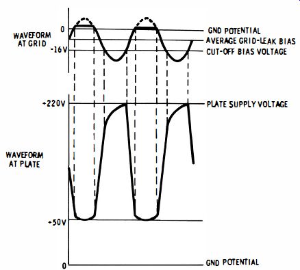
Fig. 4-16. Waveform in limiter circuit.
Signal-developed grid bias produced by grid-current flow reduces the effectiveness of the applied sine-wave voltage in driving the grid positive. This bias represents the average about which the sinusoidal variation takes place. Fig. 4-16 shows the average grid-leak bias as a negative voltage relative to ground, with the sine wave superimposed on it. When the grid is driven positive, series resistor R110 still further limits the effective signal, because of the voltage drop across the resistor due to grid-current flow. This limiting is illustrated in Fig. 4-16 by the reduction of the positive peak in the sine wave.
V102 reproduces the limited grid signal as an approximate square wave. The positive half cycles of the applied sine wave increase the plate current and reduce the plate voltage to a low value. The least positive portion of the plate waveform corresponds to the period of grid-current flow and is flattened by grid limiting. As the grid signal swings negative, plate current is reduced, and finally ceases to flow when the combination of signal and bias reaches the cut-off value. The plate voltage rises toward the supply voltage during this time. Since the input circuit of V103 is connected to the plate-load resistor through coupling capacitor C109, charging current flows in R111, which prevents the plate voltage from rising instantaneously.
Overdriven Amplifier
Although the sine-wave voltage is approximately squared by the limiter, the sides of the square wave are not as vertical as required for the production of a sharp trigger pulse. Therefore the square wave produced by the limiter tube is applied to an overdriven amplifier in order to steepen the sides of the waveform (Fig. 4-17) . The output from the limiter stage is a voltage of large amplitude. The plate current of Vl03 is cut off early in the negative alternation and is driven to a maximum early in the positive alternation. In addition, the grid current which is drawn during the positive half cycle of the applied voltage charges Cl09 through the relatively low cathode-to-grid resistance of V103. Consequently, the coupling capacitor is charged to an average voltage which acts as a high negative bias for the grid of V103.
The only bias present in the grid circuit of V103 is due to grid-current flow. Distortion in the plate waveform of V102 is caused by the charging and discharging of C109. As the grid signal of Vl03 starts to swing positive, it is ineffective until at time t1 it drives the grid above cut-off. At time t2, when the grid signal drives the grid to zero bias, grid current flows which limits the signal until t3. The grid is then swung negative, reaching cutoff at t4. Development of the plate waveform follows from the drop in voltage produced by current flow through R114. Because tube conduction takes place entirely in the positive half cycle of grid signal, the negative portion of the plate signal is narrower than the positive portion.
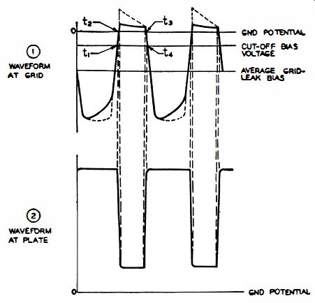
Fig. 4-17. Waveforms in overdriven amplifier circuit.
RC Peaker and Pulse Amplifier
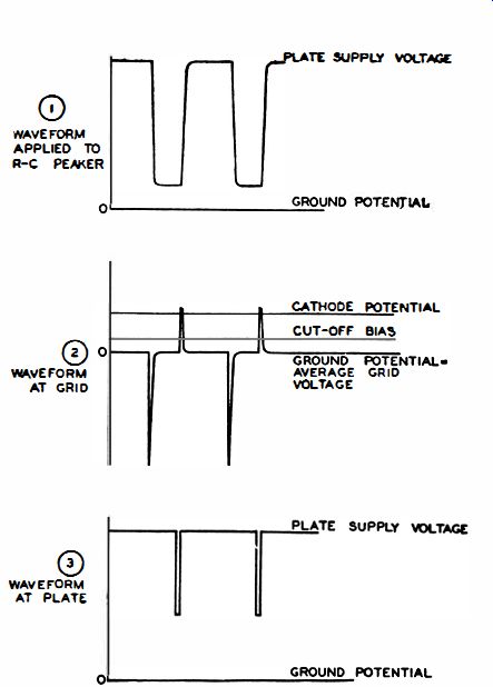
Fig. 4-18. Waveforms in RC peaker and pulse amplifier.
Output from V103 is applied to an RC peaker circuit. The important feature of the peaker is its ability to charge and discharge completely in the available time between signal alternations. The plate voltage can accordingly rise to the supply voltage only after the peaker circuit is charged. Leading edges of both positive and negative portions of the waveform are slightly rounded because of the short time utilized for charge and discharge. In order to produce a sharp pulse from the square-wave output of the overdriven amplifier, the time-constant of the coupling circuit to the following stage is made very short. Because this time-constant is so short, C111 charges and discharges completely, and the average bias produced is negligible. The grid may therefore be considered to be at ground potential. Note that the time-constant of the coupling circuit is approximately 2 microseconds for a negative voltage swing at the grid of V104 and less than 2 microseconds for a positive swing at the grid, because the low cathode-to-grid resistance shunts R116 when grid current is drawn.
When the voltage applied to the coupling capacitor rises sharply (Fig. 4-18) , a charge is quickly developed on C111. The voltage at the grid of the tube follows the charging current, rising almost instantly to its maximum value, and dropping back to zero quickly. In the same way, when the applied signal voltage swings negative, the grid is driven below ground potential, but it returns to ground quickly because C111 discharges rapidly. A series of sharp positive and negative pulses accordingly develops at the grid.
In order to eliminate the negative pulses at the input to the pulse amplifier, the tube is biased beyond cut-off. Cut-off for a 6AC7 tube with a 250-volt plate supply is approximately -6 volts. A bias of nearly 12 volts is supplied by raising the cathode potential of VI04 by means of the voltage divider R117 and R118. Using this bias, the tube does not conduct until the grid is raised to a potential of +6 volts relative to ground.
Both the negative pulses and the broad lower portions of the positive pulses are lost because of the bias on the tube. The portion of the grid signal which tends to drive the grid more positive than the cathode is limited because of the flow of grid current. The peaks of the positive pulses tend to drive the grid of V104 positive relative to the cathode, and accordingly cause a large current to flow in the tube for the duration of the pulse.
This large current flow produces a large drop of voltage at the plate of the tube, so that the output is a high amplitude negative-going pulse with a duration of approximately 2 microseconds.
Cathode Follower
In most systems of this type, the trigger pulses are conducted to the transmitter and to the CRT via coaxial cables. Cable characteristic impedances range from 50 to 150 ohms. To prevent reflections in a cable, the terminating impedance should be as nearly equal to the characteristic impedance as is practical. A cathode follower is used as a low-impedance source to feed the output pulse from the timer to the coaxial cable.
Since the trigger pulse is negative-going, it is desirable to have the cathode follower normally conduct a heavy current so that a pulse of large amplitude can be developed across the cathode resistors. The bias on V105 (Fig. 4-15) is the voltage developed across R123 by the plate current of the tube flowing through this resistor. The characteristic curves for a 6AG7 tube show that a plate current of 24 milliamperes flows in this circuit configuration. The voltage developed across R124 does not affect the bias on the tube, since it raises both the cathode and grid above ground potential.
Until the negative pulse is applied to the grid of V105, the cathode is 47 volts positive with respect to ground (1,950 X 0.024 = 47 volts) . Since the output from the pulse amplifier is more than sufficient to cut off the cathode follower, a negative-going pulse of 47 volts is produced across R123 and R124 when V105 is cut off by the applied signal. The negative pulse output from the cathode follower is fed into the coaxial lines which connect to J101 and J102.