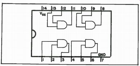
Fig. 1-1. Internal connections for the 7408 IC.
| Home | Audio mag. | Stereo Review mag. | High Fidelity mag. | AE/AA mag. |
Electronics and microcomputers in particular, could not be what we know them today, if the integrated circuit was not developed. There is no doubt, that the space age spawned the IC chip.
DETAILED IC INFORMATION
An IC is an electronic device, usually constructed from semi conductor materials, in which transistors, diodes and resistors are manufactured simultaneously to make a tiny functional electronic circuit. The IC wafer that contains the transistors, diodes and resistors may be no larger than 30 mils on a side.
For a better perspective of the integrated circuit, we need to look at the trends in the electronics industry over the past 30 years.
All electronic gear 30 years ago was built with discrete components.
These components were fabricated before being installed in the equipment and included resistors, inductors, capacitors and vacuum tubes. The gear was very bulky and heavy. It also consumed lots of power. With vacuum tube computer installations, one had to con tend with a frequent occurrence of burned out tubes and large rooms full of equipment-also, a huge electric bill.
The transistor became a direct competitor of the vacuum tube, with almost a complete take-over of equipment by 1970. At first, transistors were discrete components that were fabricated prior to their installation in electronic equipment. As semiconductor technology improved, the transistors were able to tolerate higher and operate up to higher frequencies. The higher frequency characteristic became important in the second generation of computers, which used discrete solid-state components.
The basic concepts for integrated circuits were developed during the late 1950s. By 1965, semiconductor manufacturing technology had improved so much that semiconductor firms were able to fabricate circuits on individual silicon wafers that contained many transistors. Such circuits were no longer discrete circuits.
Transistors, resistors and diodes were manufactured simultaneously 500 to 1000 at a time. These large wafers are then scribed into smaller chips that are then individually mounted into a plastic or ceramic package. The IC package is then plugged into sockets or soldered onto a printed circuit board or plug-in module.
In the late 1960s the chip makers went from the small scale integration to medium and then large scale chip integration. Small scale integration refers to integrated circuits that provide only simple gates, buffers and flip-flops. Such chips usually contain no more than 10 to 20 gates. In medium scale integration, the IC chips function as simple, self-contained logic systems such as counters, small random access memories, decoders, multiplexers and shift registers. Such chips usually contain from 20 to 100 gates. Large scale integration refers to integrated circuit chips with a complexity of greater than 100 gates or gate-equivalent circuits. Currently, many microprocessor chips contain the equivalent of several thousand gates on a single piece of silicon wafer that measures 170 mils on a side.
Probably all will agree that remarkable changes have occurred in the manufacture of semiconductor electronic devices. The cost of manufacturing a transistor within an integrated circuit has dropped to less than 0.04 cents per transistor in 1979. The technology associated with each integrated circuit transistor has also been improving. Today's gates, which are manufactured from transistors, have decreased power requirements and increased speed.
The lower the power requirement per gate, the more gates that can be placed on a small silicon wafer because of less heat to dissipate.
Today's microprocessors have almost surpassed the best large computers of the mid-1950s.
INTERNAL CHIP CIRCUIT DIAGRAMS
In order to troubleshoot digital IC circuits effectively you must know how the internal gate connections are wired to the chips pin-out leads. You will also need a diagram or symbol drawing in order to design or wire-up an integrated circuit chip. As an example, we will now look at ways to represent the internal wiring of a 7408 quad 2-input positive AND gate chip. The drawing layout pin configuration is shown in the (Fig. 1-1) drawing.
The number 7408 is assigned to all quad 2-input positive AND gate chips that have this pin configuration and the electrical specifications of the original 7408 chip, which was developed and manufactured by Texas Instruments in the late 1960s. This type of chip is available from five or more different manufacturers, including National Semiconductor, Sprague, Signetics, Stewart Warner and, of course, TI. The term quad indicates that these are four separate 2-input positive AND gates on each 7408 chip.
The positive notation refers to the fact that the gates function as AND gates when positive logic is used. Of course, negative logic may also be used with chips designed for this purpose. Finally, you will note that each gate contains two inputs; hence the 2-input designation.
Fig. 1-1. Internal connections for the 7408 IC.
Any of the 7400-series of integrated circuit chips have only two power inputs-ground (GND) and supply voltage (Vcc) input pin.
The letters V5CC represents +5 volts, although the chip should function if Vcc is anywhere in the range of +4.75 volts to +5.25 volts. If the input supply voltage goes above +6 volts, it is very likely the chip will burn out in a short time. If the power connections are reversed, and you apply +5 volts to the GND pin, and ground the Vcc input pin, they will also be burned out. Perhaps you can save the chip if you act quickly under these conditions. Remember, though, that a burned out chip (shorted) will usually be quite hot to the touch.
The pin configuration for the 7400 quad 2-input positive NAND gate chip is very similar in appearance to the 7408 IC chip, as shown in Fig. 1-2. Like the 7408 chip, the power inputs are at pin 7 and pin 14. The chip contains four independent 2-input NAND gates that can be represented as in the Fig. 1-3. Always keep in mind that none of the gates can function if power is not applied to the Vcc pin.
The drawing layout for the 7486 quad exclusive-OR gate chip is shown in Fig. 1-4. This 7486 quad contains four independent exclusive-OR gates that are represented in Fig. 1-5.
Fig. 1-2 Connections for the 7400 2-input NAND gate IC.
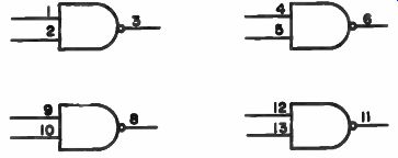
Fig. 1-3. The 7408 has four independent NAND gates.
Fig. 1 - 4. Internal layout for 7486 quad Exclusive- OR gate.
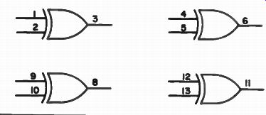
Fig. 1-5. Four independent Exclusive-OR gates are found in the 7486 chip.
DIGITAL SIGNALS AND PULSES
Digital signals are discrete or pulse signals whose various states are discrete intervals apart. The typical digital signal (Fig. 1-6) in digital electronics is a binary signal. which is defined as a voltage or current that carries information in the form of changes between two different states that are a discrete interval apart. One of these states is called the logic 0 state, and the other is called the logic 1 state. For voltage signals, the logic 0 state is typically at ground potential, whereas the logic 1 state varies between +3 and
+5 volts. For current signals, the logic 0 state is typically the absence of current 0 in A and the logic 1 state is generally set at 20 To help you visualize these logic off-on or high-low states, refer to the square-wave pulse train shown in Fig. 1-7. These states may also be referred to as zeros and ones. A gate input, to be valid, must be positive (high) or grounded (low). Thus, a key point to remember is that any gate can have only one of two possible states for its input or output logic mode. To identify these two possibilities, one state is called one and the other zero.
Almost all modern digital logic circuits are now TTL, which is the shorthand for transistor-transistor logic. Thus, the input de vices for the gates are transistors and not diodes or resistors.
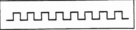
Fig. 1-6. Typical digital signal pulses.
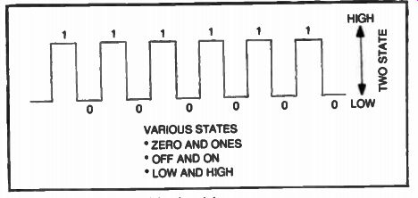
Fig. 1-7. Digital logic 0 and 1 pulse states.
These gates are referred to as DTL and RTL. Digital circuits at the block diagram level are much simpler than the analog circuits that most hobbyists are used to working with. The TTLs are two-state devices with precisely defined logic levels. The pulse drawing shown in Fig. 1-8 indicates the high and low states for TTL. When working with static logic levels, the voltmeter or scope can be used to detect high and low states. The pulse drawing indicates the 0 to 0.8 volt DC is considered to be low, while 2.4 to 5 volts DC is a high state for TTL circuitry.
The region in between is known as the undetermined state. In logic systems troubleshooting, an undefined state would usually indicate some type of circuit fault.
Each high and low pulse has a positive-going and a negative going edge. The TTL gate circuits then detect these transitions, and it is these edges that are used as the actuating signal. Only the positive-going or negative-going edge is required to make the next logic device go into operation.
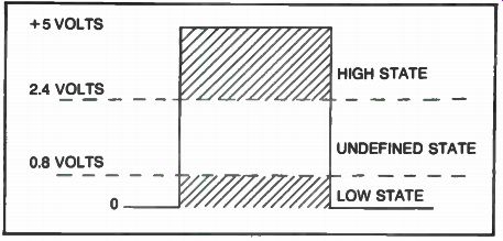
Fig. 1-8. Pulse logic levels for a TTL device.
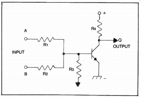
Fig. 1-9. An RTL NOR gate circuit drawing.
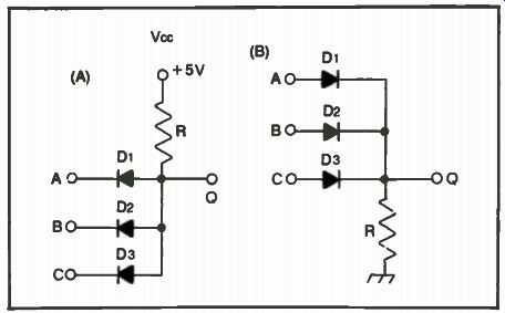
Fig. 1-10. Diode-resistor logic AND gate (A) and DRL OR gate (B).
RESISTOR-TRANSISTOR LOGIC
We will now take a brief look at the resistor-transistor logic (RTL) family of devices. The best advantage of the RTL logic is its low cost, but it has a very slow speed. RTL logic could not be utilized in the high-speed microcomputers of today. The RTL logic device consumes considerable power, has a limited drive capability and is quite noisy in operation. Its operating speeds will generally be less than 10 million counts per second.
NOR GATES Basic RTL operation can be realized with resistors and transistors alone as a NOR function. An RTL NOR gate is shown in Fig. 1-9.
The RTL NOR gate operates in this way. When both inputs A and B are low, the base-emitter junction is reverse biased and the transistor is cutoff. Thus, there is no current through R, so Q remains high. However, if one or both of the inputs are high, the base-emitter junction is forward biased; the transistor is conducting and Q now goes to a low state. The gate circuit now functions as a NOR gate.
DIODE GATES
Before we look at diode gates, let's review briefly basic diode and transistor characteristics. A diode is conducting when forward biased (when the anode is positive with respect to the cathode) and cut off when reverse biased. A transistor is conducting when the emitter-base junction is forward biased and the collector base junction is reverse biased.
The basic circuits for the AND and OR resistor diode logic gates is shown in Fig. 1-10. First, let's look at how the diode logic gate works, shown in Fig. 1-10A. In this circuit, logic 1 corresponds to +5 volt (high), and logic 0 to 0 volts (low). If all the inputs A, B and C are low, all three diodes will be conducting so that output Q will be low. In terms of positive logic, this means that when A, B and C are 0, Q is also O. And when only one or two of the inputs are low, Q is still at low.
Only when A, B and C inputs are high will all diodes be cut off so that no current can flow through R, with the result that Q is high too.
When all inputs are logic 1, the output is also logic 1. This is the correct definition for an AND function.
When we use negative logic, this circuit becomes an OR gate.
If all inputs are high (logic 0), all diodes are cut off and Q remains high. Should one or more inputs be low, the diodes in question will conduct, current will flow through R, and Q will become low (logic 1), which is the function of an OR gate.
Now let's check out the operation of the OR gate circuit shown in Fig. 1-10B with positive logic. When all inputs are low (logic 0), no current flows through R, so Q remains at ground potential (low = logic 0). However, when one or more inputs go high (+5 volts = logic 1) the diodes in question conduct, current then flows through R, and Q becomes HIGH. A DTL NAND gate is shown in Fig. 1-11.
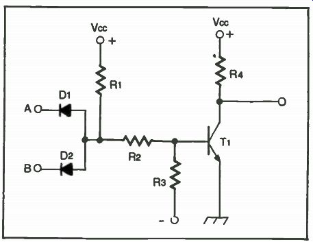
Fig. 1-11. A NAND diode-transistor logic (DTL) gate circuit.
TRANSISTOR-TRANSISTOR LOGIC
The transistor-transistor logic (TTL) family is now the most popular type of gate. Because of its high speed, it is used in all microprocessor systems. The difference between TTL and DTL logic is that instead of an input circuit made of diodes, a transistor is used. Each emitter-base diode serves as an input diode.
The basic function of the TTL gate, as with the DTL gate, is the NAND function. Refer to the totem-pole TTL logic gate circuit shown in Fig. 1-12 as we follow through this operation. If one or more inputs are at ground level (logic 0), current will flow through input resistor R1. This causes the collector of the input transistor to go low. Only when all inputs are high will the collector be high too.
The input circuit actually gives normal AND operation. The next stage acts as a type of phase splitter for driving the totem-pole output. When T2 is cut off, T4 will be on and T3 will be off, resulting in a low output, which is the NAND function. The diode in the output chain ensures that T3 is cut off when T4 goes on.
A disadvantage of the totem-pole output is that no outputs can be connected in parallel (WIRED-AND connections). If two or more TTL outputs were connected together and one output was low and the other was high, this would cause a short-circuit, and power dissipation would be much too high. However, TTL gates with special output circuits (called open collector outputs) have been designed to make WIRED-AND connections possible.
Transistor-transistor logic is commonly referred to as TTL, but may also be called T2 1. or "tee squared ell". TTL devices are low cost per gate (and going even lower). They have high-speed capabilities (20 MHz to 100 MHz is typical), good noise immunity, a moderate drive requirement. Also, hundreds of TTL devices are now available. For these reasons, most of the logic devices and troubleshooting information in this guide will deal with TTL device systems.
DIGITAL DEVICES
The dictionary definition for a digital device states that it is any system that represents data notations with exact precision. Let's see if we can bring that down to terms we can both understand.
Basically, a digital device can be defined as any device that operates on or manipulates binary. Binary refers to an operation that has two states. You may recall from previous studies that binary coding can be represented by any type of two-state device, such as an on or off light, an open or closed computer card, a north or south magnetized magnetic core or portion of a magnetic tape or disk; two different voltage levels; two different current levels; or two different frequencies. And probably the most familiar symbols are 0 (low) and 1 (high). In digital electronics, you will find devices that manipulate binary information in the form of voltage levels: +5 volts for the logic 1 state and near ground potential for the logic 0 state. With the state-of-the-art in digital electronics, a change in logic state can be accomplished in less than 2 nanoseconds. Plus the cost of digital devices are still in a nose dive. Thus, speed and low cost have caused digital devices to completely take over in the field of electronics. Some of the digital devices you will encounter in this guide are gates, counters, decoders, flip-flops, buffers, shift-registers, multiplexers, memories, encoders, latches and arithmetic/logic units.
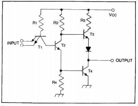
Fig- 1-12. TTL with totem-pole output gate circuit.
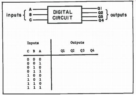
Fig. 1-13. Logic circuit with partial truth table.
The Logic Gate
Probably the most simple digital device is the logic gate. A gate is a circuit that has two or more inputs and one output. Therefore, digital information appearing at the output depends on the combination of digital information that appears at the inputs. Actually, the term gate has various meanings in the electronics field, but in this guide we will only consider the digital gate device.
The four common gates are the AND, OR, NAND and NOR gates. A gate that is more complicated can be developed from NOR or NAND gates and is called the Exclusive-OR gate. However, before we dig into gates, the truth table concept will be discussed.
Truth Table Concepts
A truth table chart shows the relationship of all output logic levels of a digital circuit to all possible combinations of input logic levels in a way that shows all circuit functions completely. By input or output logic levels, we mean logic 0 and logic 1 states, which in many digital devices contain voltage levels of 0 volts and +5 volts, respectively. The truth table definition chart may also be rephrased as follows: A truth table shows the relationship of all output logic 0 and logic 1 states of a digital circuit to all possible combinations of input logic 0 and logic 1 states so as to characterize all circuit functions completely.
Figure 1-13 shows a digital circuit that has three inputs (A, B and C) and four outputs (Q1, Q2, Q3 and Q4). The object of the truth table, then, is to give the relationships between the inputs and outputs of a logic device. This is easy since the inputs and outputs can only be zeros or ones. Since there are two possible states per each input, and there are three different inputs, this makes a total of eight different sets of inputs, which are also listed in Fig. 1-13.
On the left-hand side of the truth table you will see eight different sets of three inputs. The logic states of the four outputs will depend upon which digital gate circuits are used. You therefore, cannot complete a truth table for a given set of inputs until you know the specific circuit gates that are involved, or until the name of the specific logic device is given.
Truth tables are used because they are a simple and convenient shorthand representations of digital circuits. It is much easier to devise a truth table than to explain how a specific digital circuit operates. The more inputs and outputs that exist, the more obvious the advantage a truth table is over a written description. Truth tables are used to represent digital circuits just as electrical engineers use circuit diagrams and architects use blueprints for buildings. Truth tables actually show the behavior of digital circuits and represent many words of explanation.
Gates and Their Use
The digital gate functions can be used in many different ways.
However, no matter how a gate is used, the truth table for the gate will always apply. A truth table is a basic characteristic of a gate.
Thus, it is not altered no matter how a gate is used.
A gating circuit is one in which a gate is used to control the passage of a digital signal, which may be a single pulse, a group of pulses, or a train of pulses.
A logic circuit is an electronic circuit that provides an input output relationship corresponding to a Boolean algebra logic function.
A memory is any device that can store logic 0 and logic 1 states in such a manner that a single bit or group of bits can be accessed and retrieved. Memory elements can be constructed from groups of gates that are referred to as flip-flops.
OR Gate Operation. You will find the symbol and truth table for the OR gate in Fig. 1-14. For the OR gate, the unique state occurs when both input A and input B are at logic 0. This observation is important whenever you want to remember the truth table for an OR gate. Thus, the unique output state, logic 0, occurs when all inputs to an OR gate are at logic 0.
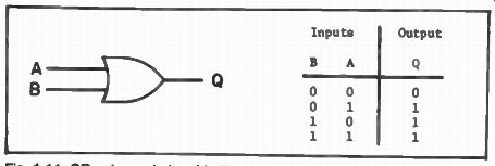
Fig. 1-14. OR gate symbol and truth table.
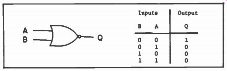
Fig. 1-15. The 2-input OR gate and truth table.
NOR Gate Operation. A NOR gate is a binary circuit with two or more inputs and a single output, in which the output is logic 1 only when all inputs are logic 0, and the output is logic 0 if any one of the inputs is logic 1. The symbol and truth table for the 2-input OR gate is shown in Fig. 1-15.
At this time, we need to note the small circle (on the point of the cone) in the OR gate symbol. This small circle has been shown previously in the NAND gate symbol. In other words, for the NOR gate, you can treat the inputs as those to an OR gate, and then invert the output. A 2-input NOR gate can be created from a 2-input OR gate and a single inverter, as shown in the Fig. 1-16. Or a 2-input OR gate can be developed from a 2-input NOR gate plus an external inverter. Please keep in mind that inversion, or complementation, can be represented either by the inverter symbol or by the small circle placed before or after a gate or other type of digital device symbol.
The Exclusive-OR Gate. The Exclusive-OR gate can be easily defined by looking at its symbol and truth table in Fig. 1-17.
This type gate is closely related to the OR gate, and is sometimes called an Inclusive-OR gate by computer programmers. The only difference between the two occurs when both input A and B are at logic 1. For the OR gate, the output is logic 1, whereas for the Exclusive-OR gate, the output is logic 0. When multiple-input OR gates are used occasionally, the Exclusive-OR gate is typically a 2-input gate.
Exclusive-OR gates are common and can be purchased as integrated circuit chips that contain four such gates on a single chip.
Alternatively, a single Exclusive-OR gate can be built from three 2-input NAND gates and a pair of inverters, as shown in Fig. 1-18. If you remember the truth table for the NAND gate and inverter, you can readily demonstrate that this circuit produces the truth table for an Exclusive-OR gate.
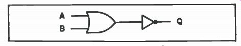
Fig. 1-16. A 2-input NOR gate created from a 2-input OR gate and an inverter.
AND-or-INVERT Gate. The AND-or-INVERT gate is a composite gate circuit that is used in microcomputer systems. This is not a basic gate. It actually consists of AND gates and a single NOR gate. Such gates are available with two per integrated circuit chip. When you use an AND-or-INVERT gate, you must specify how many AND gates are included and how many inputs each AND gate possesses. For a 3-wide 2-input AND-or-INVERT gate, this indicates that there exists three AND gates, each of which has two inputs. The symbol and truth table for a 2-wide 2-input AND-or INVERT gate are shown in Fig. 1-19.
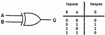
Fig. 1 - 17. Exclusive- OR gate with its truth table.
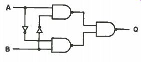
Fig. 1-18. An Exclusive-OR gate made from three 2-input NAND gates and a pair
of inverters.
Buffer/Driver Device. A buffer gate or driver is a digital device that increases the power or current handling capability of a binary circuit that is connected to the buffer gate or driver. It is a binary circuit with one input and one output in which the output is logic 0 when the input is logic 0, and the output is logic 1 when the input is logic 1. This should not be called a buffer gate, as there is only a single input. Refer to Fig. 1-20 for the symbol and truth table for a noninverting buffer/driver device.
The output voltage from a buffer or driver is usually +5 volts or at ground potential. Some devices could have more than +5 volts on them. In these cases, the buffer/driver circuits cannot be connected directly to the inputs of other IC chips without damage.
Some Complex Gating Circuits. Many varied and complex digital electronic devices can now be readily obtained from many IC electronic manufacturers. Some of these devices are available at low cost and are IC chips that contain many complex gating circuits, such as decoders, full adders, multiplexers, arithmetic logic units/ function generators and priority encoders.
One example of a complex gating circuit is the truth table and gating circuits for the TI 7442 BCD-to-decimal decoder chip shown in Fig. 1-21. To construct such a circuit, 10 4-input NAND gates, 4 inverters and 4 inverter/buffers are required. This is all fabricated on a single integrated circuit chip. An example of an even more complex gating integrated circuit is the 74181 arithmetic logic unit/ function generator shown in Fig. 1-22, courtesy of Texas Instruments Incorporated. If you study this IC carefully, you will observe AND-or-INVERT gates, Exclusive-OR-gates, inverters, 4-input NAND gates, and 4-input AND gate. This entire circuit is available on a single integrated circuit chip.
In some ways the more complex digital electronics that go into a chip, the easier it is to troubleshoot these systems. The more circuitry within a chip, the less external wiring and components you will have to replace or check out.
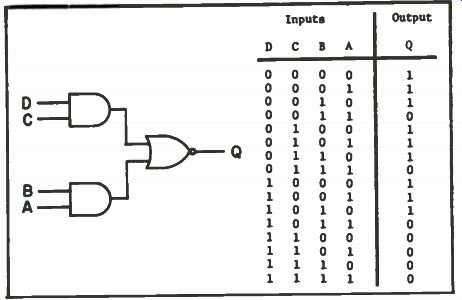
Fig. 1-19. A 2-wide 2-input AND-OR-INVERT GATE.
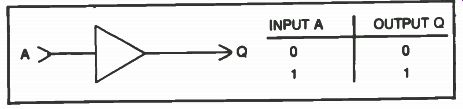
Fig. 1-20. Noninverting driver and truth table.
Fig. 1-21. A TI 7442 BCD-to-decimal decoder chip and truth table (courtesy
of Texas Instruments).
Fig. 1-22. The T174181 arithmetic logic unit/function generator chip (courtesy
of Texas Instruments).
Standard Gate Symbols. The most common standard gate symbols will now be discussed and illustrated. In order to make logic troubleshooting easier, you should try to commit these basic gate symbols to memory.
The following gate symbol drawings will be found in Fig. 1-23: 2-input AND gate, 3-input AND gate, 2-input NAND gate, 3-input NAND gate, 2-input OR gate and 2-input NOR gate.
A more complicated gate, such as the Exclusive-OR gate, which can be constructed from 2-input NAND or NOR gates, is shown in Fig. 1-24. The symbol for an inverter, which is a single input single-output digital device, is shown in Fig. 1-25. The symbol for a buffer, sometimes referred to as a driver, is shown in Fig. 1-26.
AND Gate Operation. The behavior or operation of a 2-input AND gate can be stated as follows: If input A is logic 1 and input B is logic 1, then output Q is logic 1. With any other input combination, output Q is logic 0. To help you with the truth table for an AND gate, remember the unique output state: Logic 1 occurs when all inputs to an AND gate are at logic 1. Figure 1-27 shows the AND gate and its accompanying truth table.
Fig. 1-23. Various gate symbols for reference.
Fig. 1-24. The Exclusive-OR gate symbol.
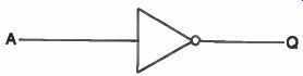
Fig. 1-25. Inverter symbol.
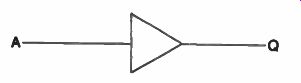
Fig. 1-26. Buffer or driver symbol.
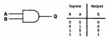
Fig. 1-27. Symbol for AND gate and its truth table.
3-Input AND Gate. The operation of a 3-input AND gate is stated as follows: If input A, input B and input C are all at logic 1, then output Q is also logic 1. For all other input logic combinations, output Q is at logic 0. The symbol for the 3-input AND gate and its accompanying truth table are shown in Fig. 1-28. We can now define an AND gate as a binary circuit with two or more inputs and a single output, in which the output is logic 1 only when all inputs are logic 1, and the output is logic 0 if any of the inputs is a logic 0. NAND Gate Operation. A NAND gate can be defined as a binary circuit with two or more inputs and a single output, in which the output is logic 0 only when all inputs are logic 1, and the output is logic 1 if any one of the inputs is logic 0. The NAND gate is closely related to the AND gate. The one difference is that the output of the NAND gate is the complement of the output of a related AND gate. The symbol and truth table for the 2-input NAND gate are shown in Fig. 1-29.
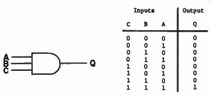
Fig. 1-28. A 3-input AND gate and truth table.
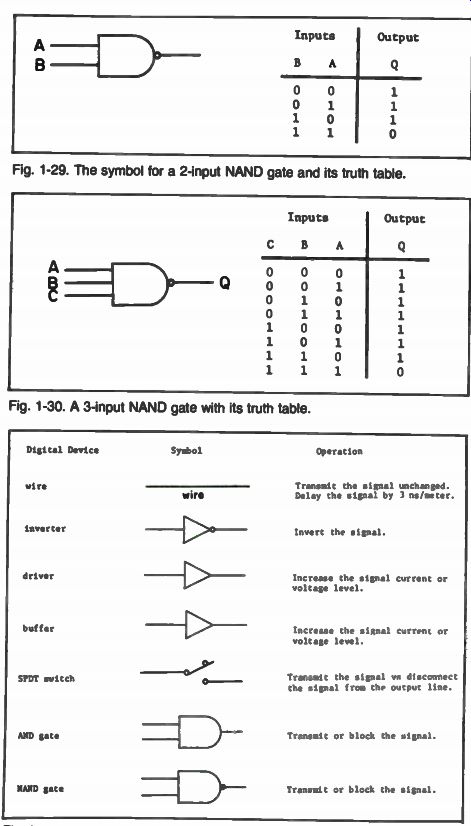
Fig. 1-29. The symbol for a 2-input NAND gate and its truth table.
Fig. 1-30. A 3-input NAND gate with its truth table.
Fig. 1-31. Various electronic devices and the operations they perform on digital signals.
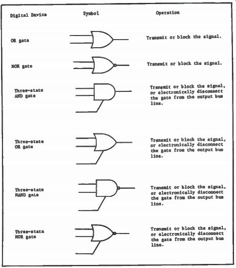
Fig. 1-32. Selected devices and the functions they perform on digital signals.
If you compare the NAND gate with the AND gate, they will be the same except for the outputs. A logic 1 for an AND gate is a logic 0 for a NAND gate and a logic 0 for an AND gate is a logic 1 for a NAND gate. Logic 1 and logic 0 are said to be complements of each other. Logic 1 is the complement of logic 0, and logic 0 is the complement of logic 1. Figure 1-30 shows the symbol for a 3-input NAND gate and its truth table.
OR Gate Operation. An OR gate is a binary circuit with two or more inputs and a single output, in which the output is logic 0 only when all inputs are logic 0, and the output is logic 1 if any one of the inputs is logic 1. The behavior of a 2-input OR gate can be stated as follows: If input A is logic 1 or input B is logic 1, then output Q is logic 1. If both inputs are logic 0, then Q will be logic 0 also. Included in this statement is the condition when both input A and input B are logic 1, in which case output Q is also logic 1.
The information and device drawings shown in Figs. 1-31 and 1-32 are useful as references when troubleshooting any digital/logic equipment. These reference charts give representative operations that will be performed upon digital signals.