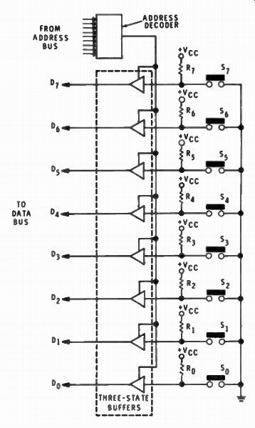
Fig. 2-3. Keyboard interfacing switches.
| Home | Audio mag. | Stereo Review mag. | High Fidelity mag. | AE/AA mag. |
In this section we will look at some of the terms and definitions for digital computers, data processors, microcomputers and the 'microprocessor. At this stage of the game, it is not easy to pin down a correct definition for any of these terms.
Many digital devices are called computers or data processors.
Data processors are generally used not only to compute, but also to perform other functions with data that flows to and from them. As an example, data processors are used to gather data from various sources, rearrange it, and then print the data. These operations do not use arithmetic manipulation that we usually associate with a computer, but the computer term is still applied to this application anyway. Thus, the definitions for computer and data processor have been loosely used for quite some time.
DATA PROCESSOR TERM
The definition for a data processor is a digital device that processes data. It might be a computer. But it can also be used to gather, distribute, digest, analyze and perform other data operations. These operations would not necessarily be computational.
The term for data processor is narrow, while the definition for computer covers a broad field.
THE MICROPROCESSOR VERSUS THE MICROCOMPUTER
Is the definition for microprocessor and microcomputer one and the same? The answer could be yes or no, depending upon whom you are talking to at the moment.
A microcomputer or small computer is a complete working system. The small computer would contain a microprocessor chip, memory, clock, input/output (I/O) ports, power supply and other support devices. The term microprocessor therefore describes an extremely small electronic system that is capable of performing specific tasks. I am sure that in the near future a complete microcomputer will be fabricated on a single chip, including memory and I/O ports. Each day sees newer and more powerful microprocessor chips come on the market. From the preceding observations, a microprocessor is not a microcomputer, but is only a part of one.
A microprocessor, then, is the control and processing portion of a small computer or microcomputer. And it is usually referred to as the type of processor built with LSI-MOS (large-scale integration-metal-oxide semiconductor) circuitry that is usually all in one chip. Like all computer processors, microprocessors can handle both arithmetic and logic data in bit-parallel fashion under control of a program. These are both distinguished from a minicomputer processor by their use of LSI with its lower power and costs of other LSI devices by their programmable behavior.
BINARY CODES
Computer binary codes are referred to as alphanumeric codes because they are used to represent both numbers and characters.
The most common codes you will hear in computer jargon are hexadecimal, ASCII and Baudot. We'll discuss two of them.
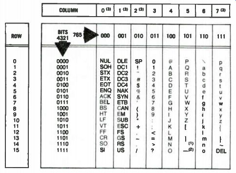
Table 2-1. The 7-Bit ASCII Code.
The ASCII Code
The most popular computer coding scheme is known as the American Standard Code for Information Interchange and is refer red to by the letters ASCII. The letters ASCII are pronounced as-key. ASCII is a special form of binary code that is used with microprocessors and data communications systems. (Another code name that is gaining in popularity is the American National Standard Code for Information Interchange (ANSCII). ASCII is a 7-bit binary code that is used to transfer data between the microprocessor and its peripheral or I/O devices. A serial ASCII code referred to as RS232C is used for communicating data by radio and telephone.
With six bits, a total of 2 to the power of 6, or 64 different characters can be represented. These characters make up decimal numbers 0 through 9, the alphabet upper-case letters, along with the other characters used for punctuation and control. The full or extended 7-bit ASCII code is represented by a total of 2 to the power of 7 or 128 different characters. The 7-bit ASCII contains lowercase letters of the alphabet and additional characters for punctuation and machine control. The 7-bit standard ASCII code is shown in the Table 2-1.
In a microcomputer, the text or information is stored as a sequence of bits (binary digits) and is referred to as a string. When the text is printed out, the bits are fetched in the proper sequence and transmitted to a video display or printer. Logic associated with the display or printer interprets the binary data of the characters it represents. If the text is entered via a keyboard, as a particular key is depressed the binary digit code associated with that key is transmitted to the microcomputer. The "micro" then stores this code in the appropriate memory bank. The standard ASCII and hexadecimal character codes are shown in Table 2-2.
Baudot Code

Table 2-2. Standard Character Code.
The Baudot code is a binary code that has five binary digits to represent a character, such as five rows of holes on punched paper tapes with each row capable of representing a single character. This Baudot code is used in standard commercial teletypewriter transmissions involving the use of punched paper tape.
The standard five-channel teletypewriter code consists of a start impulse and five character impulses, all of equal length, and a stop impulse whose length is 1.42 times longer.
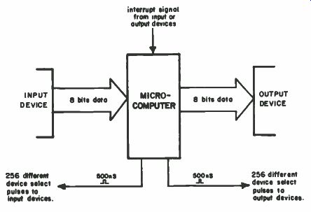
Fig. 2-1. The four principle tasks of interfacing: input, output, device select pulse generation and interrupt servicing.
SYSTEM INTERFACING
Interfacing can be defined as joining a group of devices so they work in a compatible manner, including memory and I/O ports.
Some terms used with interfacing are as follows:
• Synchronous or sync-in step or in phase, as for two devices. For a computer this would be a performance of a sequence of operations as controlled by clock signals or pulses.
• Synchronous operation-system operation under the control of clock pulses.
• Synchronous logic-type of digital logic used in a system in which logical operations take place in synchronism with clock pulses.
• To synchronize or sync in-to lock one element of a system into step with another.
• Sync pulses-pulses developed at transmitting equipment and introduced into the receiving equipment to keep both systems operating in step.
• Synchronous inputs-those inputs of a flip-flop that do not control the output directly, as do those of a gate, but only when the clock permits and commands.
Although the details of computer interfacing vary with the type of microcomputer used, the general principles of interfacing apply to a wide variety of microcomputers. For the 8080A microprocessor, the basic objectives of interfacing are summarized in Fig. 2-1.
The objectives of microcomputer interfacing are as follows:
III Synchronize the transfer of 8 bit of data between each input device and the microcomputer.
• Synchronize the transfer of 8 bits of data between the microcomputer and each output device.
• Generate the appropriate input and output data transfer sync pulses, which are called device select pulses. For an 8080A-based microcomputer, 256 different input sync pulses and 256 different output sync pulses can be generated.
• Service interrupt signals that enter the microcomputer from external I/O devices.
• Program the microcomputer to perform all input and interrupt servicing operations.
Interface Busses The block diagram in Fig. 2-2 gives you another view for three of these interfacing busses. Briefly, the transfer of 8-bits of data between the CPU and an I/O device occurs over the 8-bit bidirectional data bus. The specific I/O device that is involved in the data transfer is selected Via the use of 8-bits on the address bus. The precise timing of the data transfer is determined by the presence of an IN or OUT pulse on the control bus. Thus, during the transfer of data between the CPU and I/O device, all three busses are participating.
INPUT/OUTPUT DEVICES
What is an I/O device, you may ask? It is any digital device, including a single integrated circuit chip, that transmits data to, or receives data or strobe pulses from, a microcomputer.
Usually you would think of an I/O device as a large, complex unit. Some of these large I/O devices are CRT terminals, card readers, modems and line printers. However, a single IC chip, such as a latch, tri -state buffer, shift register, or small memory, can be classified as an I/O device.
The transfer of data between a microcomputer and an I/O device must be synchronized, and this is accomplished with pulses called device select pulses. We should point out that several device select pulses may be required for a single I/O device. In one example, a 74198 shift register has a pair of control inputs that determine whether the register shifts left or right, or parallel loads eight bits of data. The chip also contains clock and clear inputs.
Thus, a single 74198 chip may require three or four unique device select pulses. You can generate 256 different input device select pulses and 256 different output device select pulses, but this does not mean that you can address 512 different devices. A more reasonable number is somewhere between 50 and 100 devices.
Rarely would you need this many device select pulses. If need be, design changes can be made to generate more select pulses.
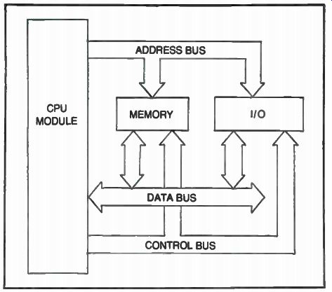
Fig. 2-2. Block diagram showing three interfacing busses.
Interface Switches and Contact Bounce
When data is sent into the microprocessor via keyboard or microswitches, these un-debounced pulses will give spurious spikes when changing from one logic state to another. Keyboard interfacing switches are shown in Fig. 2-3. The spurious pulses-note waveform shown in Fig. 2-4-are a consequence of contact bounce at the switch contacts. Just about all switches produce contact bounce. When the switch is closed, the contacts do not make a positive electrical or mechanical connection, but bounce open and closed for a short period of time.
Fig. 2-3. Keyboard interfacing switches.
Microswitches and rotary switches all exhibit contact bounce when changed from position to position. The closing of a switch is not an action that can be accomplished in a few microseconds. It occurs over a period of milliseconds to hundreds of milliseconds.
Thus, it is just the nature of mechanical switches that they will bounce. Contact bounce may only last for a few milliseconds, but that is long enough for the MPU (microprocessing unit) to believe that the bounces are also switch contact closures. To solve this contact bounce problem, some switches use cross-coupled NAND gates that instantly latch onto one state, which ignores all contact bounce. Of course, this will require some additional circuitry.
A much better design scheme would be to let the MPU itself do the debouncing. A technique that is often used is to wait about ten milliseconds and then read the data from the switch-bank again. If the same data is read, then the MPU can be certain that the switch is closed. The switch contacts can be checked or poled as many times as required until contact bounce is eliminated. Always keep these points in mind and be on the alert for contact bounce which could cause glitches in the program that give false information during microcomputer system troubleshooting.
THE INTEL 8080A MICROPROCESSOR
The 8080A is a complete 8-bit central processing unit (CPU). This N-channel microprocessor is fabricated on a single large-scale integrated (LSI) chip. The 8080A has many control and processing applications. In order for you to visualize the complexity of this micro, a magnified photo of this chip is shown in Fig. 2-9.
The 8080A contains six 8-bit general purpose working registers and an accumulator. Note the functional CPU block diagram in Fig. 2-6. The six general-purpose registers may be addressed individually or in pairs providing both single and double precision operators. Arithmetic and logical instructions set or reset four testable flags. A fifth flag provides decimal arithmetic operations.
There is also an external stack feature wherein any portion of memory may be used as a last in/first out stack to store or retrieve the contents of the accumulator, flags, program counter and all the six general-purpose registers. The 16 bit stack pointer controls the addressing of this external stack. This stack gives the 8080A the ability to easily handle multiple-level priority interrupts by rapidly storing and restoring processor status. It also provides almost unlimited subroutine nesting.
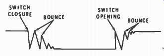
Fig. 2-4. Waveform caused by contact bounce.
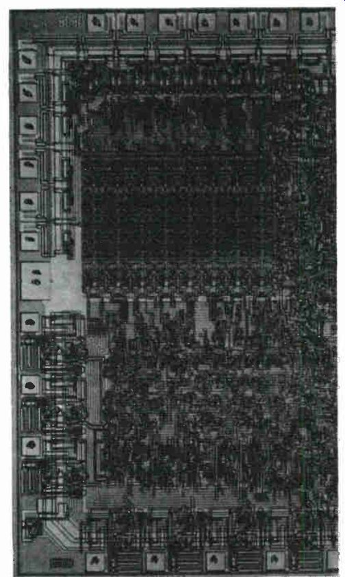
Fig. 2-5. Magnified photograph of the 8080A microprocessor chip by Intel
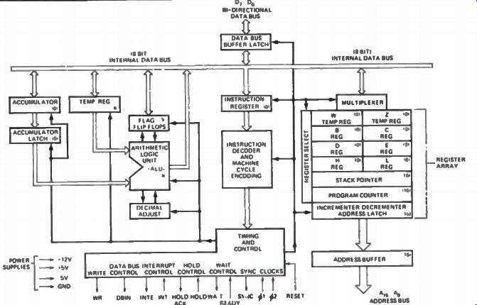
Fig. 2-6. Functional block diagram of the Intel 8080A CPU.
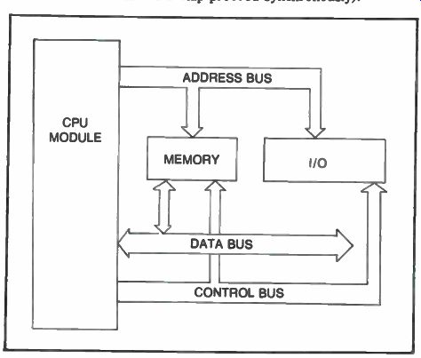
Fig. 2-7. Simple block diagram of the Intel 8080A CPU.
This microprocessor chip has been designed to simplify the complete systems design of the computer. Separate 16-line address and 8-line bidirectional data busses are used to facilitate easy inter face to memory and I/O. Signals to controls the interface to memory and I/O are provided directly by the 8080A. Ultimate control of the address and data busses resides with the HOLD signal. It provides the ability to suspend processor operation and force the address and data busses into a high-impedance state. This permits OR-typing these busses with other controlling devices for direct memory access (DMA) or multiprocessor operation.
Some 8080A Chip Requirements The simple block diagram of the 8080A microprocessor chip is shown in Fig. 2-7. A typical microcomputer designed from an 8080A chip possesses all of the minimum requirements for a digital computer, which are as follows:
• It is programmable, with the data and program instructions capable of being arranged in any sequence desired.
• It is digital.
• It is clocked (in most microcomputers, the internal operations in the CPU chip proceed synchronously).
• It contains an arithmetic/logic unit located within the CPU chip, that performs arithmetic and logic operations.
• It can exchange data with memory or I/O devices.
• It contains fast memory. Speed is an important requirement for a functional digital computer.
Address Bus for the 8080A Micro Chip
The 8080A micro chip has a 16-bit address bus that is used for identification of specific memory locations or specific I/O devices.
This is an unidirectional bus, with only address information coming out of the 8080A chip. When addressed, 65,536 different memory locations can be accessed. The 8080A is a 64K device, where the K indicates kilobyte, or 1024 bytes.
The address bus is also used to supply the 8-bit device code for input and output devices. When addressing input-output devices, the address bus will assume another identity. Thus, it is subdivided into two identical 8-bit device code bytes, which are used as inter face circuits to I/O devices. When addressing I/O devices using the IN or OUT microcomputer instructions, 256 different input and output devices can be addressed.
When working on a bus problem, you should be aware of the possibility that different types of information appear on the bus line at different times. This is the case with the 8080A address bus system. Most of the time the information that appears on the address BUS is the address of a specific memory location. Occasionally, the information that appears on the address BUS is a device code. The microcomputer knows when the BUS is being used to access memory and when it is being used to identify I/O devices, as it provides the appropriate control pulse which informs you what it is doing. Always keep these control pulses in mind when troubleshooting these bus systems.
Bidirectional Data Bus
The 8080A chip contains an 8-bit bidirectional data bus that permits eight bits of data, known as a byte, to be transferred between the micro chip and memory or I/O device. Much of the time, data that appears on the data bus is an instruction byte from memory. At other times, the data that appears on the data bus is one of the following:
• A data byte that is being input from an input device.
• A data byte that is being output to an output device.
• A data byte that is being written into or read from memory.
• Control status bits used to derive some of the control bus signals.
• A HI or LO address byte that is being stored in an area of memory called the stack.
• A HI or LO address byte that is being retrieved from the stack.
• An instruction byte that is being jammed by an I/O device during an interrupt.
The microprocessor provides the appropriate control or status pulses that inform you about the type of activity currently in progress.
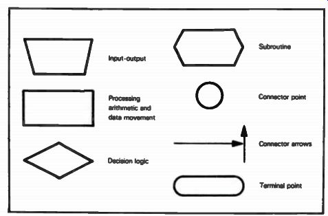
Fig. 2-8. Some standard flowchart symbols.
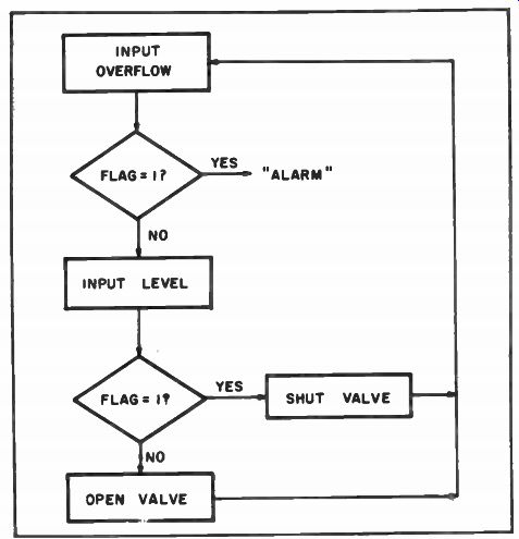
Fig. 2-9. A system flow chart for controlling the level of a liquid in a storage
tank.
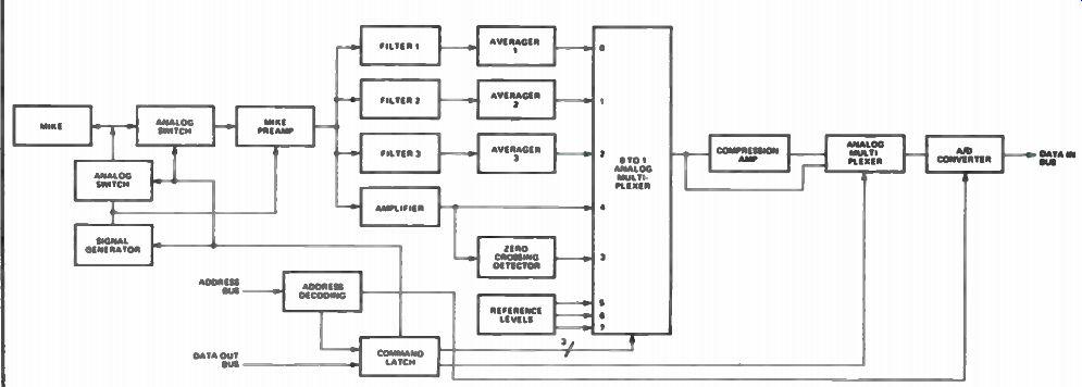
Fig. 2-10. Block diagram of the Speech-Lab model 50 speed recognition peripheral.
FLOWCHARTS
A flowchart is a schematic diagram for the flow of information through the various components that make up the microprocessor system. This flowchart can be used as a map by the technician when troubleshooting systems that can be quite complex. As the systems program is being developed and debugged, the design engineer will usually draw a flowchart. Many times the flowchart will be drawn before any program is written. The flowchart is a most important way of documenting an operational program. The chart in Fig. 2-8 shows some of the more common or standard flow diagram symbols. These symbols are used to distinguish the various classes of operation from input to output of the system. As an example of how these symbols are used, Fig. 2-9 shows a system flowchart for controlling the level of solvent in a storage tank.
MINICOMPUTER SPEECH ENTRY APPLICATIONS
Data entry into the home microcomputer via the human voice is now possible on a limited scale at low cost. In the next few years, a technological breakthrough is a certainty. Of course, Bell Laboratories and Carnegie-Mellon university are developing new ideas each day in regards to voice input to computers and related knowledge of voice patterns or speech recognition. Also, the high density and low cost of the bubble magnetic memories now coming on stream will greatly increase the vocabulary of these speech recognition systems.
One voice control unit, now available at a low cost for the home microcomputer is the Speechlab system by Heuristics, Inc. of Los Altos, CA. The Speechlab system can be plugged into any microcomputer, with an S-100 bus and will directly control the various programs. Some of the computer brand names are SOL, Vector Graphics, Altair, Imsai, Byte, Inc. and many others. Also, it can be adapted for use with other computer systems. The assembled Speechlab comes with a complete hardware system, including a high fidelity microphone. The PC (printed circuit) board unit is ready to plug into the S-100 bus of the computer to start someone on voice control programs. Also included is a complete hardware and Speechlab Laboratory manual.
Let's now take a brief review of this speech system's technical features. The Speechlab offers 64 bytes of storage for each spoken word, has real time response, and is 95-percent correct in its recognition. The system is capable of handling a 64-word vocabulary, and also features the latest CMOS design for reliability and low power consumption. Typical power consumption is about 1 watt.
The Speechlab system features functional signal processing modules so that they can be reconfigured under software control for maximum freedom. Filter skirt rolloff is 80 db per decade. The unit also has a signal generator for prompting and built-in tests that are usually only found in more expensive equipment. Another feature is the single input/output port. A block diagram of the model 50 Speechlab system is shown in Fig. 2-10.
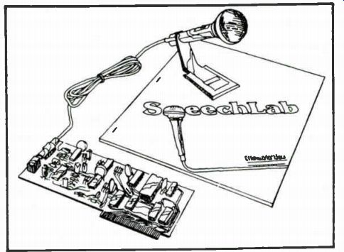
Fig. 2-11. The model 20A by SpeechLab speech recognition peripheral.
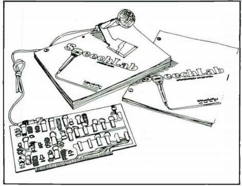
Fig. 2-12. The SpeechLab model 50 speech recognition peripheral.
Hardware includes three band-pass filters (6 bits amplitude), one zero crossing detector, a linear amplifier, compression amplifier, 6-bit AID converter and a beeper. The raw waveform is available for advanced experiments.
Software includes seven complete programs, three of which are offered in source and on paper tape and four in source alone. The ones on paper tape and source include a Speech Basic programming language, an assembly language speech recognition program and a hardware self-test program. Source programs are a Speech Basic plot, a Speech Basic correlation, a Speech Basic recognition and a Speech Basic advanced recognition.
The Speechlab model 20 shown in Fig. 2-11 has a vocabulary of 32 words. The model 20S is used in computers with the S-100 bus.
The model 20A works with the Apple II small computer system.
The model 20 features ROM based software with a re-locatable program which lets you load anywhere into memory with a vacant spot. After loading, the 2K ROM can be disabled under computer control. The speech recognition program, callable from any BASIC, requires 4K bytes of user-supplied RAM. This RAM can be located anywhere in the address space. Model 20 hardware includes two band-pass filters with 2 bits of amplitude, two zero crossing detectors and a linear amplifier. The Speechlab model 50 that plugs into a S-100 bus computer system, such as a SOL-20, is shown in the Fig. 2-12.
SPEECHLAB MODEL 20
HARDWARE OPERATION
The SpeechLab model 20 hardware consists of a microphone amplifier with frequency compensation, two analog band-pass filters, each with a signal rectification/averaging stage, a zero crossing detector, a 1K byte ROM and logic to run the input port and the ROM memory interface. Figure 2-13 shows a block diagram of the model 20, Fig. 2-14 shows a schematic diagram of the circuit.
Microphone Preamp
The first element in the signal chain is the microphone, which produces an analog signal on the order of 10 millivolts for normal speech. The first stage of the microphone preamp pre-emphasizes signals up to 3.1 kHz at a rate of 6 dB per octave. That is, high-frequency signals are amplified more than low-frequency signals, with the rate of gain increase being a factor of two for each doubling in frequency up to 3.1 kHz. From 3.1 kHz to 6.6 kHz, the gain of the amplifier is constant, and the gain drops off beyond 6.6 kHz at the rate of 6 db per octave. This preemphasis compensates for the characteristics of the human vocal tract, which produces less energy in the higher audio frequency ranges than in the lower frequencies. The pre-emphasis tends to make all frequency components have the same order of magnitude. The output of the first stage feeds the second stage, which simply amplifies the first stage output by a factor of 60. The microphone preamp output is biased such that the output rests at about 5.5 volts with no signal into the preamp, and swings about this reference voltage by ±5.5 volts, utilizing the full dynamic range of 0 to 11 volts.
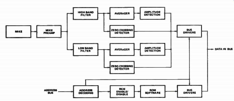
Fig. 2-13. Block diagram of the SpeechLab model 20A speech recognition peripheral.
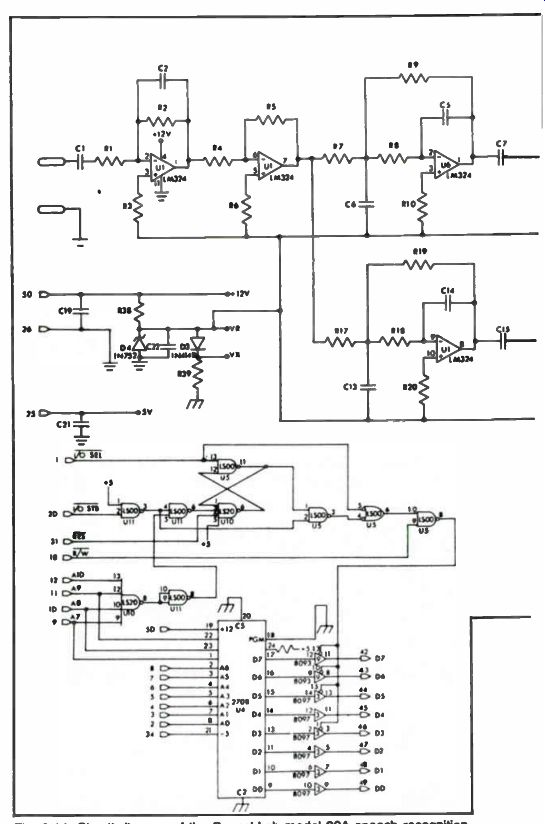
Fig. 2-14. Circuit diagram of the SpeechLab model 20A speech recognition peripheral.
Filters
The output of the microphone preamp feeds two audio band pass filters. These filters amplify and extract that portion of the speech utterance which falls within the frequency bandpass of the filter. The first filter has a frequency bandpass range of 150 Hz to 900 Hz; the second filter ranges from 900 Hz to 5 kHz. The lower frequency band corresponds to the frequency range of the lowest frequency resonance (formant) of the human vocal tract, and the higher frequency band corresponds to the frequency band of the next two vocal tract resonances. The energy and frequency in each of these frequency ranges is determined by the shape of the vocal tract which, of course, varies with time to produce time-varying outputs from these filters during a speech utterance.
The band-pass filters are each implemented as a cascade of a second-degree multiple feedback low-pass filter followed by a second-degree multiple feedback high-pass filter to yield attenuations of 40 db/decade (12 db/octave) above and below the pass bands. The outputs of each filter are biased to the reference level of 5.5 volts. That is, in the absence of any signal, the output will rest at 5.5 volts, and in the presence of a signal will swing above and below that level. Each filter output produces sine waves proportional in amplitude and equal in frequency to the output of the microphone signal that falls within the frequency bandpass of the filter. The output of each filter is fed to a zero crossing detector and a rectifier/averager.
Zero Crossing Detector
The zero crossing detectors provide a means of measuring the dominant frequency component of the signal passing through each of the filters. The zero crossing detector is a comparator with one input connected to the reference voltage and the other input connected to the filter output. Because the filter output is equal to the reference voltage (5.5 V) when no signal is input to the microphone, the two comparator inputs are equal when no signal is present.
When a signal is present, however, the output of the filter will swing above and below the reference voltage. When the filter output is above the reference voltage, the comparator will be forced to a logic zero output. When the filter output is below the reference voltage, the comparator is forced to a logic one state. Every time the filter output crosses the reference voltage, the comparator changes state. The output of each comparator is connected to the parallel output port, where they can be input to the computer. The computer reads the zero crossing detectors and determines the number of times the comparator changes state, from one to zero or vice versa, in a given time period. This number is equal to the number of times the filter output crosses the reference voltage level. If the input to the filter were a single sine wave, the number of state changes in one second would be exactly twice the frequency, because a sine wave crosses the reference voltage twice in one period. Speech waveforms typically have several frequencies present with one frequency dominant. The dominant frequency in a frequency range is equal to the resonant frequency of the vocal tract in that frequency range. The other frequencies are attenuated by the vocal tract. The addition of small amplitude waves on the dominant wave causes sinusoidal ripples in the dominant wave. These ripples sometimes occur as the dominant wave passes through the reference voltage level at the output of the filter, producing additional zero crossings compared to the number produced by the dominant wave alone. The difference, though, is small and of little consequence. The output of the filter is also fed to a rectifier/average stage.
Rectifier/Averager
The rectifier/averager circuit produces an output proportional to the amplitude of the sine waves coming from its associated filter. This is accomplished by rectifying the filter output relative to the reference voltage and time averaging the result. The rectification is implemented with a diode, which only passes current to the aver ager when the filter output is above the reference voltage. The time averager is a low-pass filter (leaky memory) with a bandwidth of 20 Hz. In the absence of new signals from the filter, the averager will decay to its no-signal value, the reference voltage, with a time constant of 50 milliseconds. Thus the averager forgets events which occurred 50 milliseconds in the past. The output of the averager is a voltage proportional to the energy of the waveform from its associated filter. The output of the rectifier/averager is fed to the amplitude detection hardware.
Amplitude Detection
Amplitude detection is simply accomplished by comparing the output of the rectifier/averager stage with three fixed voltages using three voltage comparators. One of the comparator reference voltages is set very close to the no-signal output of the rectifier/ averager to determine the beginning and ending of words. The other two reference voltages are set at about one-third and two thirds of the dynamic range of the rectifier/averager outputs. These comparator outputs, three for each of the two frequency bands, are routed to the parallel input port where they can be input to the computer.
ROM Enable/Disable
The ROM enable/disable circuitry operates in accordance with the rules for Apple II computer peripherals with on-board ROM. The I/O select signal from board connector pin 1 enables the on-board ROM whenever the processor executes a memory read instruction to read from the 256-byte block of memory set aside for each peripheral card. This address block is CNO0 to CNFF where N is the peripheral connector slot number, 1 to 7. Once a memory read instruction from this address block has occurred, an RS flip flop is set to enable mode, which allows the on-board 1K-byte ROM to occupy half of the full 2K-byte address space from C800H to CFFFH set aside for any peripheral. This range is detected via the I/O strobe signal which decodes this address range on the Apple H mainframe. The ROM will remain enabled until a memory access is made to the address range CF8OH to CFFFH, or until a reset occurs, whichever happens first.