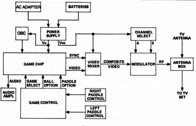
Fig. 11-1. Block diagram for the Radio Shack model 60-3051 video game.
| Home | Audio mag. | Stereo Review mag. | High Fidelity mag. | AE/AA mag. |
Games that people now play on the screens of TV sets are of course well known as video games. These games operate with digital logic pulses that simulate the playing field lines, the game ball and the players instead of the analog video now used for TV station signals.
The digital video is added to the vertical sync, horizontal sync and blanking to make up the composite video. This video information modulates an oscillator (rf unit) and is usually on either channel 3 or 4 for TV set operation. The modulated carrier goes through a TV/GAME SELECTOR switch before being fed to the TV antenna terminals. The modulated video game signal operates the TV receiver the same as any TV station or cable channel signal. Thus, any standard TV receiver may be used with no modification necessary.
Many of these video games use LSI (large-scale integration) ICs that have hundreds of transistors and diodes which cut down considerably on the required components.
CLOCK CIRCUITS
To operate the video game, a clock generator is needed. The clock generates a square wave signal that is used as a reference for all other circuit systems. The square wave is called the clock signal and is often produced by a multivibrator circuit.
In this section we will check out one of Radio Shack's video games and at some troubleshooting information and tips on this unit.
Next we will see how the RCA Studio II video game operates and how to use the test cartridge for complete check-out procedures of this system. The section concludes with information on the Motorolas MC1372 color TV video modulator chip used in video games, color generator test instruments and video tape recorders.
RADIO SHACK MODEL 60-3051 VIDEO GAME
The Radio Shack TV game is divided into six major subsections. They are the game chip, power supply, video mixer, oscillator, modulator and audio amplifier.
Shown in Fig. 11-1 is a block diagram of the TV game electronics. The power supply provides power to all sections. The game chip develops all video signals and processes the ball and paddle options, as well as receiving game selections from the selector switch. This IC performs all of the game functions. All other sections and components support this main game IC. The crystal oscillator section feeds the master reference frequency of 2.01216 MHz to the game chip. The video mixer section accepts the five video outputs from the game chip and makes one composite waveform that is then fed to the modulator. The modulator, as its name implies, amplitude modulates the video information onto the carrier frequency. This carrier is of the proper frequency so that TV channel 3 or 4 can be used to receive the games. The audio amplifier section current-amplifies the audio generated by the game IC to drive the speaker.
Fig. 11-1. Block diagram for the Radio Shack model 60-3051 video game.
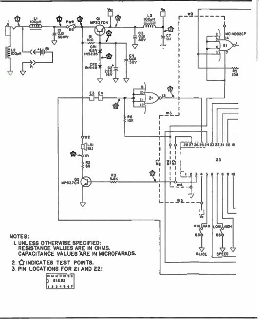
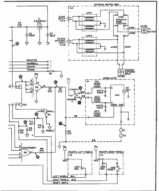
Fig. 11-2. Complete schematic of the Radio Shack model 60-3051 video game.
VIDEO GAME TROUBLESHOOTING
The following test equipment is required for video game troubleshooting:
-- Oscilloscope-30 to 50 MHz (triggered) and a low capacitance (LC) probe.
-- Digital voltmeter (DVM).
-- Frequency counter (optional).
Refer to Fig. 11-2 for a complete schematic of the video game as we look at some troubleshooting information.
Power Supply
If the video game does not operate at all, the power supply would be the prime suspect. Apply 9.0 VDC to the input and check for 6.5 VDC at TP5. If TP5 passes the test, move on to the oscillator circuit. If TP5 fails, check for 7.1 VDC at TP4. If an improper voltage is found, check CR1 and CR2 for proper operation. Also check capacitor C2 for shorts. If TP4 tests good, then Q1 may be defective.
Transistor Q 1 will be destroyed (open) if there is a short on the V line, even momentarily. If the fault is not found, continue to trace back to TP3 (unregulated power to the audio and regulation section), switch S6, TP2, TP1 and finally to J1.
The value of capacitor C2 is multiplied by the gain of Q1 and a much larger capacitor is "electrically" connected at TP5. If the capacitor were opened or completely left out of the base circuit, little effect would be noticed with game operation when using batteries. However, with AC operation, hum bars might be seen on the TV screen. Hum bars usually show up as dark bands that drift up or down the screen. These bars are caused by ripple voltage from the rectified AC which will distort the video waveform. The action of C2 and Q1 help eliminate ripple to less than 0.01 volt. Note that hum bars can also be caused by the power supply in the TV set used for the game display.
Hum bars may be tolerable on the screen when viewing TV programs, but with video games that have straight vertical and horizontal lines, hum bars can become objectionable. Usually, ripple will cause distortion of the vertical lines by putting a small bend in them. It will be your analysis to determine if the hum bars are a defect in the game console or in the TV set monitor.
Crystal Oscillator
A square wave of 2.01216 MHz should be found at TP8. The CMOS gate used as the active portion of the oscillator is operating as a linear device and not as a digital device. Consequently, the square wave will have sloping rise and fall times, and slightly rounded logic levels. Note the oscillator circuit shown in Fig. 11-3.
Instruments used to measure the frequency or analyze the waveform should have a high impedance and less than 50-pF capacitance.
Problems that could prevent the oscillator from working could be a shorted capacitor, open PC runs, a defective IC, or a bad crystal. Pins 2, 3 and 4 of Z1 must be tied to ground for the circuit to operate. R5 must be present since this resistor sets up the bias for Z1. R4 could be shorted and the oscillator would still work, but if R4 were to open, the oscillator would not work. Also check L3 for an open since it supplies power.
MOS Game Circuit
You should handle (CMOS chip) with care. If possible, handle it by the case and do not touch the leads. A static charge could damage the IC. Because all game functions and video signal are generated by Z3, the major problems with the game will usually be associated with Z3 or the controlling circuitry. Check for power Vc voltage, Ve voltage and power ground points of Z3. If they are OK, check TP9 for a high (almost Vc). If TP9 is low (almost ground), Z3 is held in reset all the time and it will appear not to function. The circuitry associated with TP9 is part of Z1, R6 and reset switch A3S1. If TP9 appears low all the time, measure the voltage at TP10 (use a high-impedance voltmeter or scope). If this point is low, then either Z1 is bad, or there is an open or short along the PC runs of Z1. If TP10 is high, then check A3S1. It could be operating such that it is closed all the time or its contacts could be bent and therefore shorting.
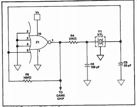
Fig. 11-3. Crystal oscillator circuit.
Audio Amplifier
The audio output from Z3 is at pin 3 or TP11. The tone burst goes from a ground level to Vc level. If you see tone action at TP11 and the speaker is not beeping, check for proper operation of Q2. If Q2 is OK, check for poor solder joints around R2. If R2 is also OK, check the speaker for continuity and check the associated PC board runs. Notice that the audio network receives its power from the unregulated side of Q1.
Video Processing
The video processor NOR gate Z2 inverts, mixes and buffers all video and sync signals for the modulator. The sync signals at TP13 are easily seen with an oscilloscope, but the video at TP14 is difficult to see unless you have a scope with high vertical amplifier gain. The best test for this section is the TV set itself. Since left and right players (paddle) video, ball video and the score and field video are all outputted on separate pins of Z3, it is a simple matter to determine what pin you would suspect is opened or shorted if the ball or paddle is missing from the screen.
An open input to Z2 would probably be harder to isolate than a shorted (to ground) pin. For example, let's say pin 5 of Z2 (left player video input) is shorted to ground. The TV screen will show a normal video pattern, except the left player paddle will be missing.
If pin 5 of Z2 is open (or shorted to Vcc), the TV screen will appear to be synced up properly but there will be no video at all. An open or short to Vcc on pin 2, 3, or 4 of Z2 would cause this same blank field.
Notice that the sync half of Z2 has all its inputs tied together.
All we need here is an inverter and not a mixer. Pin 16 of Z3 is normally high. During vertical and horizontal time, pin 16 of Z3 goes low. This means that pin 13 of Z2 goes high during sync time, but is held low during video time.
Mixing the video and the sync pulses together is handled by R7, R8, R9 and R10. If you look at TP15 with an oscilloscope, you will find a composite video signal of about 4 volts peak-to-peak. The video levels are from 0 volts to about 2 volts. The sync levels are from 2 volts to about 4 volts. R9 and R10 form a single voltage divider network that chops this 4 volts down to less than 2 volts, which is the maximum that should be applied to the modulator.
Problems with these resistors will usually be limited to poor solder joints or PC board run problems.
Modulator
Due to FCC requirements, the modulator unit should not be repaired. If you find proper voltages, grounds and video levels entering the modulator and there is no picture on the TV screen, replace the modulator.
Antenna Switch Box
Except for opens or shorts, about the only problem you should find in the switch box is loose components. Make sure all devices have good solder connections and that all hardware is tight and making good ground connections. Insure that the internal shielding within the box is not shorting any wires. Also, make sure that the rivets holding the shielding, the terminal strip and isolation switch are tight. The best test for the switch box is actually connecting it to a TV monitor and feeding video into it. Check for picture sharpness and any show that would indicate a weak signal.
Remote Paddle Controls
Problems with the remote paddle controls should be limited to wiring problems within the cables and problems with switches and controls. Electrical problems may show up as disappearing paddles, or there may be a "no man's" area on the screen where the paddles are hard to control or position in this area. Also, make sure that the paddle controls will move the paddles all the way off the screen in both directions. If capacitors C9 and C8 are open, then the waveform at TP 19 will be a negative-going pulse with no ramping of the waveform.
Refer to Table 11-1 for more troubleshooting information.
Also, the schematics for the Radio Shack model 60-3052 video game is shown in Fig. 11-4.
-------------------
Table 11-1. Troubleshooting Chart.
INDICATION
Audio OK but no picture
Picture faded, no contrast control, audio OK Paddles jerk more than 1" every time speaker beeps Audio weak, good picture Dead game. no audio or video Picture OK but no audio Picture OK but hum bars present i when AC adapter is used.
No ball, score or field Picture is OK, but no Paddles
Picture shows hockey and 5 paddles all the time in one or all game positions No speed. slice or paddle options No picture on Channel 3, OK on' Channel 4 Picture on Channel 3 and Channel 4 Picture OK, but weak diagonal lines present Audio on for too long a time after ball rebound Paddle jitters at random rate
PROBABLE FAULT Antenna Switch Box Modulator Video Mixer Video Mixer Power Supply Audio Section Power Supply Oscillator Reset Circuit Audio Section Power Supply Video Section (video)
Video Section (video)
Game Select Switch Chip Control Modulator Control Modulator Control Antenna Switch Box Audio Section Power Supply
LOOK FOR
Broken coax A4S1 not in Game position.
Box not property connected to TV. Open Al L1 or A1 L2 Open AlL3.
Bad Z2 or an open or shorted PC connector.
Z2 not MC14002BCP (MC14002CP is not to be used for Z2). Weak batteries AC line too low (AC Adapter) Short in audio section Intermittent L1 or L2 Shorted CR2 Defective 01 R2 not of proper value-
02 defective Speaker defective Open 01 Shorted C2 Shorted CR1 Open S6 or Li Broken J1.
Shorted PC runs Shorted C6 or C5 Open input to Z3 Bad Z1 or V1 Bad solder joints Jumper broken or missing.
A3S1 shorted Z1 or Z3 bad.
Open or shorted 02 Opened LS1 Bad solder pints or PC runs.
Open C2 Bad 01 or CR1 Z2 is bad or the input is shorted Z3 not reset. Press the reset button.
Z2 bad or shorted Z3 not reset. Press the reset button A2R1 or A3R1 bad or wrong position C8 or C9 opened Bad solder joint on R12, Rh
S2 bad or bad ground PC run short.
Bad switch (S3, S4. S5) PC run short or open.
Si bad Modulator bad Modulator coil open.
St bad or solder short Modulator power in put shorted.
Broken balun coil.
Bad switch.
Open ground.
Missing jumper wire (Pin 3 to 27) on Z3 C7 opened or missing.
---------------------------------------
RCA STUDIO II VIDEO GAME
The RCA Studio II home video game programmer uses the COSMAC microprocessor, along with a plug-in memory, to provide a versatile game and educational format. The complete Studio II system is shown in Fig. 11-5.
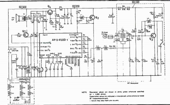
Fig. 11-4. Schematic for the Radio Shack 60-3052 video game.
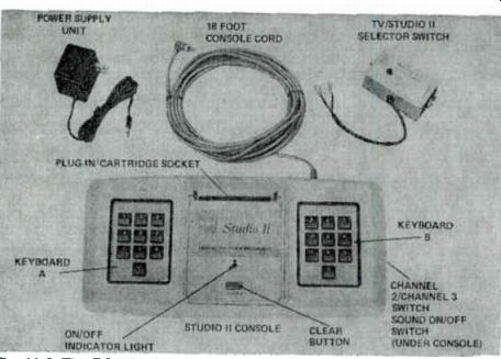
Fig. 11-5. The RCA Studio II game system.
Studio II uses RCA's single-chip version of the COSMAC microprocessor, the CDP1802, which provides central computer control for the various game, educational, and other entertainment programs. Thus, a very high level of program sophistication can be achieved, limited only by the solid-state memory capacity. The system remains flexible and can be updated through the expedient use of plug-in program cards. The Studio II's logic is based on the modified FRED system. The complete unit connects to the VHF antenna terminals of a standard television receiver. Two, 10-digit keyboards located on the main housing let the players control the display and select the game to be played.
The system has three major units as follows. The main-control console contains the keyboards and electronics for selecting and processing the programs. The selector switch box controls power to the control console and connects either the TV antenna or the rf output cable from the game to the receiver antenna terminals. The power supply plugs into the wall AC outlet and supplies 9 VDC to the control console via the selector switch box and rf output cable.
Supplementing the programs built into the fixed ROM of the control console, some plug-in cartridges have been programmed with additional entertainment formats.
System Operation The game system can be divided into eight sections:
• Microprocessor.
• Memory system consisting of read-only memories (ROMs) and random-access memories (RAMs).
• Player/keyboard interface.
• Video display generator.
• Sound circuit.
• rf oscillator/modulator section.
• Selector switch box.
• DC power supply.
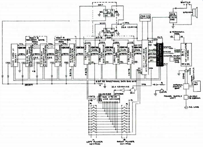
Fig. 11-6. The Freeway test display.
The heart of Studio II is RCA's type CDP1802 COSMAC microprocessor. The CDP1802 is an LSI CMOS, 8-bit, register oriented CPU. For this application, it is operated at 5 VDC and at a clock frequency of 1.760 MHz.
When the CLEAR button is pressed, the microprocessor registers are reset. A game is selected from the ROMs by entering the proper code via the key pad buttons. The game starts as the microprocessor executes the program instructions contained in the ROMs.
The Memory
The memory has 2048 bytes of ROM and 512 bytes of RAM. For programs contained in the resident or external ROM memory devices, 1024 bytes of ROM are used as an interpreter language.
The interpreter ROM provides common game display patterns, score keeping, subroutines, etc. The remaining 1024 bytes of ROM are mask-programmed resident game formats. The RAMs are used for TV refresh, stack and variable storage. Data bytes can be written into the RAM (memory write, MWR) or readout of the RAM (memory read, MRD) on command of the microprocessor.
When a program cartridge is plugged into the control socket, the resident memory (ROM) is deselected and operation proceeds by using the cartridge memory (ROM).
The Keyboards
Two 10-key pads provide the player/keyboard interface. The key pads were specifically developed for the RCA Studio II video game. The keys are arranged in the standard telephone-type for mat. Keyboards were selected in lieu of other ways of player interface because they provided the flexibility of permitting specific numerical entries as well as motion and direction entries.
System Test Procedures
Press the CLEAR button on the console and then press key 4 on the left-hand keyboard. This sets up the game for Freeway, and the track as shown in Fig. 11-6 should appear immediately. If necessary, adjust the fine tuning and hold controls of the TV for best picture.
Operational Checks With The Test Cartridge
The test cartridge, which plugs into the cartridge slot on the Studio II console, scans the digital circuitry for trouble with a routine that takes about 30 seconds. If it finds a malfunction, this will be indicated on the TV screen. If there is no trouble, the cartridge sets up a test for the two keyboards. Note that when using the test cartridge, use a 500-mA power supply.
Press and hold the CLEAR button on the Studio II console.
Insert the Tester 1 cartridge into the slot while holding the CLEAR button. Now release the CLEAR button. A pattern similar to that in the top of Fig. 11-7 should appear on the screen immediately, and Tester 1 begins its scan of the system (indicated by the black streak moving through the white field in the lower half of the pattern). If the pattern fails to appear or a pattern other than that shown appears, a defective chip is indicated.
In about 11 seconds, the first scan is complete. The display shifts to the second pattern shown in Fig. 11-7 with a white streak scanning a black field. This scan takes another 11 seconds. At the end of the second scan, the system changes the pattern on the lower half to a series of transient vertical white lines on black and then a series of black lines on white. This sequence takes about two seconds. At the end of this short sequence, the pattern shifts to the third pattern shown in Fig. 11-7. This indicates that all memories are operational. A digit or digits appearing in the checkerboard pattern in the center of the screen, as shown in the bottom pattern of Fig. 11-7 indicates chip failure in the PC board.
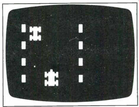
Fig. 11-7. Various Tester 1 screen patterns.
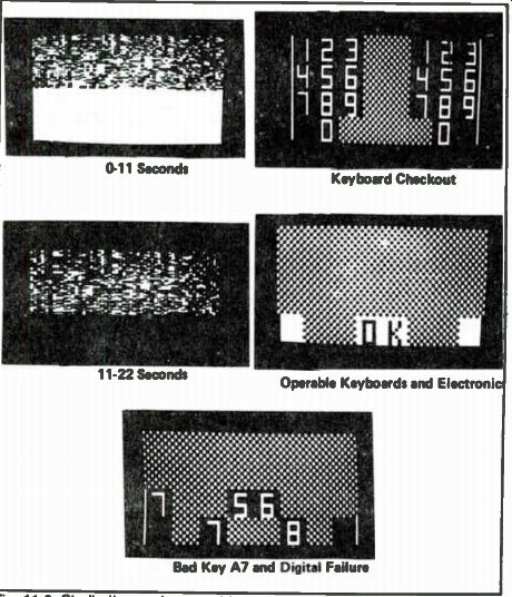
Fig. 11-8. Studio Il console assembly.
If the checkerboard appears as in the third pattern, touch the keys-one at a time-of the keyboard A, and then keyboard B. As each key switch closes, the digit on the screen should change to a checkerboard square. If any digit remains on the screen after the key is pressed, the keyboard is defective and must be replaced.
When all key closures are complete (indicating satisfactory keyboard function), the video screen shifts to the OK pattern as shown in the fourth pattern. The pattern flip flops between black on-white and white-on-black until the CLEAR button is actuated. If the CLEAR button functions normally, the whole sequence starts again as the button is released. This is the complete Studio II Tester 1 test program that is performed with the test cartridge. A complete exploded view of the Studio II console assembly is shown in Fig. 11-8.
MOTOROLA VIDEO MODULATOR MC1372 CHIP
The Motorola MC1372 chip can be used with video games to generate rf TV signals from color-difference and luminance signals.
Referring to the block diagram in Fig. 11-9 we see the MC1372 contains a chroma subcarrier oscillator, lead and lag networks, chroma modulator, an RF oscillator and modulator and a TTL compatible clock driver with adjustable duty cycle. This color TV video modulator IC is also used in test instruments and video tape recorders.
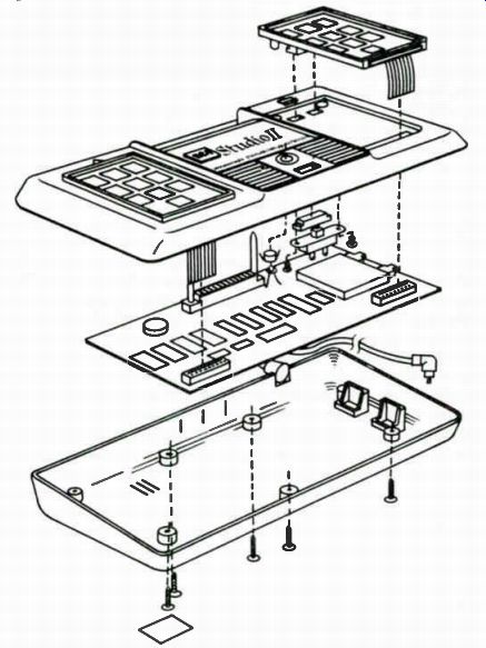
Fig. 11-9. Block diagram of the MC 1372 integrated circuit (courtesy of Motorola).
Operational Description and Chip Pinout
Refer to the circuit of the MC1372 chip in Figs. 11-10 and 11-11.
Pin 1-Clock Output. This provides a rectangular pulse output waveform with a frequency equal to the chrominance subcarrier oscillator. The output is capable of driving one LS-TTL load.
Pin 2-Oscillator Input. This is the color subcarrier oscillator feedback input. The signal from the clock output is externally phase-shifted and AC-coupled to this pin.
Pin 3-Duty Cycle Adjust. A DC voltage applied to this pin adjusts the duty cycle of the clock output signal. If the pin is left unconnected, the duty cycle is approximately 50 percent.
Pin 4-Ground.
Pin 5-Color B Input. This is a DC-coupled input to chroma modulator B, whose phase leads modulator A by approximately 100 degrees. The modulator output amplitude and polarity correspond to the voltage difference between this pin and the color reference voltage at pin 6.
Pin 6-Color Reference Input. The DC voltage applied to this pin establishes the reference voltage to which color A and color B inputs are compared.
Pin 7-Color A Output. This is a DC-coupled input to chroma modulator A, whose phase lags modulator B by approximately 100 degrees. The modulator output amplitude and polarity correspond to the voltage difference between this pin and the color reference voltage at pin 6.
Pin 8 -Chroma Modulator Output. This is a low-impedance (emitter-follower) output which provides the vectorial sum of chroma modulators A and B. Pin 9-Luminance Input. This is the input to the RF modulator. This pin accepts a DC-coupled luminance and sync signal.
The amplitude of the rf signal output increases with positive voltage applied to the pin, and ground potential results in zero output. A signal with positive-going sync should be used.
Pin 10- Chrominance Input. This pin supplies input to the rf modulator and accepts AC-coupled chrominance provided by the chroma modulator output (pin 8). The signal is reduced by an internal resistor divider before being applied to the rf modulator.
The resistor divider consists of a 300-ohm series resistor and a 500-ohm shunt resistor. Additional gain reduction may be obtained by the addition of external series resistance to pin 10.
Pin 11-V. Positive power supply.
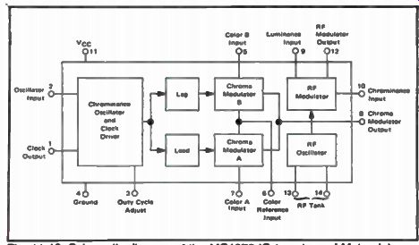
Fig. 11-10. Schematic diagram of the MC1372 IC (courtesy of Motorola).
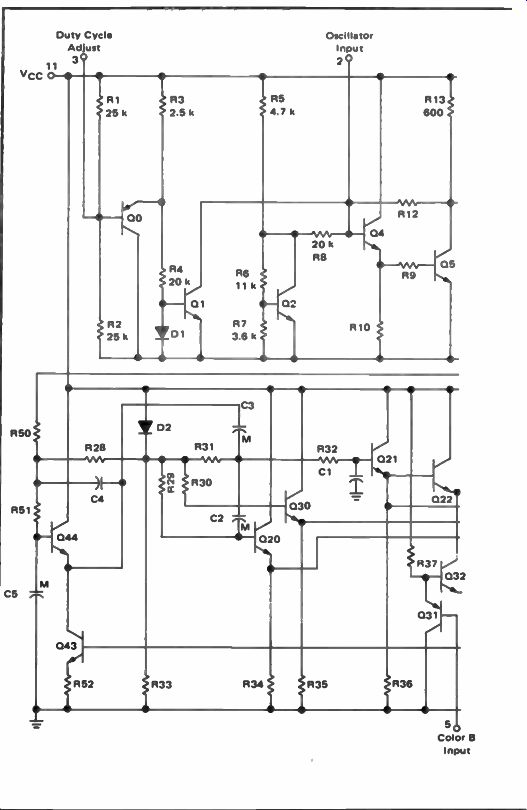
Fig. 11-11. Typical application circuit block diagram for the MC1372 video
modulator chip (courtesy of Motorola).
Pin 12-RF Modulator Output. This is the common collector of the output modulator stage. Output impedance and stage gain may be selected by choice of register connected between this pin and the DC supply.
Pins 13 and 14-RF Tank. A tuned circuit is connected between these pins to determine the rf oscillator frequency. The tuned circuit must provide a low DC resistance shunt. Applying a DC offset voltage between these pins results in base-band compo site video at the rf modulator output.
MC1372 Circuit Description
The chrominance oscillator and clock driver consists of emitter-follower Q4 and inverting amplifier Q5. The signal presented at clock driver output pin 1 is coupled to oscillator input pin 2 through an external RC and crystal network, which provides 180 degree phase shift at the resonant frequency. The duty cycle of the output waveform is determined by the DC component at pin 1 internally coupled through R12 to the base of Q4. As pin 1 DC voltage increases, a smaller portion of the sinusoidal feedback signal at pin 2 exceeds the Q4 base voltage of two times VBE required for conduction. As the DC level is reduced, device Q4-and thus Q5-is turned on for a longer time of the cycle. Transistors Q0, Q1, Q2 and diode D1 provide the biasing network that determines the DC operating level of the oscillator. The transistors Q2 and resistors R5, R6 and R7 form a voltage reference of four times VBE at collector of Q2. The DC voltage at pin 1 is determined by the value of R4, R8 and R12, and the applied duty cycle adjusts the voltage at pin 3. Since these resistors are nominally equal, the voltage at pin 1 will always approximate the DC voltage at pin 3.
The oscillator signal at pin 1 is internally coupled to active filter Q44. This filter reduces the frequency content above 4 MHz. The output of the filter at the emitter of Q44 is AC-coupled through C3 to the input of lead/lag network. R32 and C1 provide about 50 degrees of phase lag, while C2 and R29 provide about 50 degrees of phase lead. These two quasi-quadrature waveforms are used to switch chroma modulators B and A, respectively. The transistors Q22 through Q25 and Q32-33 form a doubly balanced modulator. The input signal fed to pin 5 is compared to the color DC reference voltage applied at pin 6 of the differential amplifiers. The source current provided by Q34 is partioned in Q32 and Q33 according to the differential input signal. The bases of transistors Q23 and Q24 are connected to the DC reference voltage at the emitter of Q30. The base of transistors Q22 and Q25 are connected to the phase delayed oscillator signal at the emitter of buffer transistor Q21. The differential signal currents provided by Q32 and Q33 are switched to transistors Q22 through Q25, and the resultant signal voltage is developed across R49. This signal has the phase and frequency of the oscillator signal at the emitter of Q21. The amplitude is proportional to the differential input signal applied between 5 and 6.
Transistors Q26 through Q29 and Q38 and Q39 form chroma de modulator B. This modulator develops a signal voltage that is proportional to the differential voltage applied between pins 6 and 7.
The phase and frequency of the output is equal to the phase advanced chroma oscillator at the emitter of the buffer transistor Q20. Both chroma modulators A and B share the same output resistor, R49, so the output signal presented at the emitter of Q42 (pin 8) is the algebraic sum of modulators A and B. The rf oscillator consists of differential amplifier Q18 and Q19 cross-coupled through emitter followers Q16 and Q17. The oscillator will operate at the parallel resonant frequency of the network connected between pins 13 and 14. The oscillator output is used to switch the doubly balanced rf modulator, Q9 through Q15. Transistors Q7 and Q9 provide level shifting and a high input impedance to the luminance input at pin 9. The bases of transistors Q9 and Q10 are both biased through resistors R17 and R18, respectively, to the same DC reference source voltage at Q6 emitter. The base voltage of Q10 may only be offset in a negative direction by luminance signal current source Q8. This design insures that overmodulation due to the luminance signal will never occur.
The chrominance signal developed at pin 8 is externally AC coupled to pin 10 where it is reduced by resistor dividers R20 and R17 and added to the luminance signal in Q9. The resultant differential composite video currents are switched at the appropriate rf frequency in Q12 through Q15. The output signal current is presented at pin 12. Transistors Q36 and Q41 and resistors R44 and R47 provide a highly stable voltage reference for biasing current sources for transistors Q43, Q34, Q35 and Q11.
-------------------