Fig. 8-1. Playback chroma signal process circuit CX-136A.
| Home | Audio mag. | Stereo Review mag. | High Fidelity mag. | AE/AA mag. |
In this section we will touch on a few selected digital logic and PLL circuits found in video play/record machines. We will also be looking at servo controls and tracking systems.
SONY VCR SYSTEM
This section will cover the SONY VCR Betamax format and helical scan system. Information on the chroma signal processor and modulator section will be dealt with. Then we will look at record/ play head timing pulses, servo controls and tracking systems.
Chroma Signal Processing
The chroma record signal is processed with IC2 (CX-133A) which is located on the YC-L board that is located on the bottom of the machine. The chroma record system operates as a record acc (automatic chroma level control), as a color killer and performs the frequency down conversion to 688 Hz. Referring to the block diagram in Fig. 8-1, you will see that the video signal is fed to a 3.58-MHz bandpass filter at the same point where the chroma signal is separated.
The filter output is then fed to the acc gain-controlled amplifier.
This circuit is similar to the acc control range in some TV chassis.
This amplifier controls the gain to keep the burst signal at a constant level.
Fig. 8-1. Playback chroma signal process circuit CX-136A.
The acc output goes to a frequency converter and burst gate circuit. Also going to this circuit is a delayed horizontal sync input pulse. This opens the burst gate at the proper time to allow only the burst through. This burst signal is then coupled to the burst transformer and then to a crystal ringing filter circuit which converts the burst signal to a CW signal. The amplitude of this CW signal is proportional to the amplitude of the burst signal and is fed into pin 6 of IC 2. The normal 3.58-MHz CW signal is shown in Fig. 802. The filtered CW signal is then amplified to a level high enough to drive the acc detector circuit. The acc peak detector detects the CW signal and compares it with the reference voltage to obtain an error voltage. The acc output level is adjusted by changing the reference voltage. In essence, the converted chroma signal recorded on the tape retains the same level relationship as did the original chroma signal. If the recorded video tape chroma level is different from the original TV program (color too strong or too weak), this circuit may be defective.
The scope can be used to check for waveforms shown on the block diagram in Fig. 8-1. A video signal should be found at pin 13 of IC2. A delayed horizontal sync pulse is at pin 10. The 3.58-MHz CW signal is at pin 6. And a 4.27-MHz input signal is at pin 16. There should also be a 3.58-MHz chroma output at pin 18 and a 688-kHz chroma output at pin 15 of IC 2. If all input signals check correctly on the scope, then IC 2 could be defective. Of course, make sure that all DC power-supply voltages are correct.
Chroma Playback
In playback mode, the rf signal is received from the rf playback amplifier. This signal contains both the chroma and Y-FM signal.
This signal is routed through a low-pass filter, which rejects the Y-FM signal, extracting only the 688-kHz chroma signal.
The 688-kHz signal is fed to an acc gain-controlled amplifier.
The DC voltage, obtained by detecting the playback burst signal, is fed to the gain-controlled amplifier. A feedback loop thus formed adjusts the gain of the acc amplifier so that the burst signal level remains constant. Because separate capacity stage circuits for the acc detection output are provided for each channel, the acc loops are independent for each of the two heads, so no chroma output level is noted, even if a large level difference exists between the two head outputs.
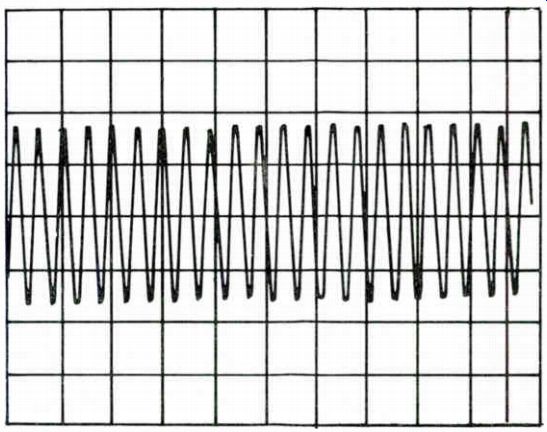
Fig. 8-2 Normal 3.58 MHz CW signal.
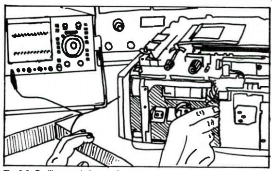
Fig. 8-3. Oscilloscope being used to check out the VCR.
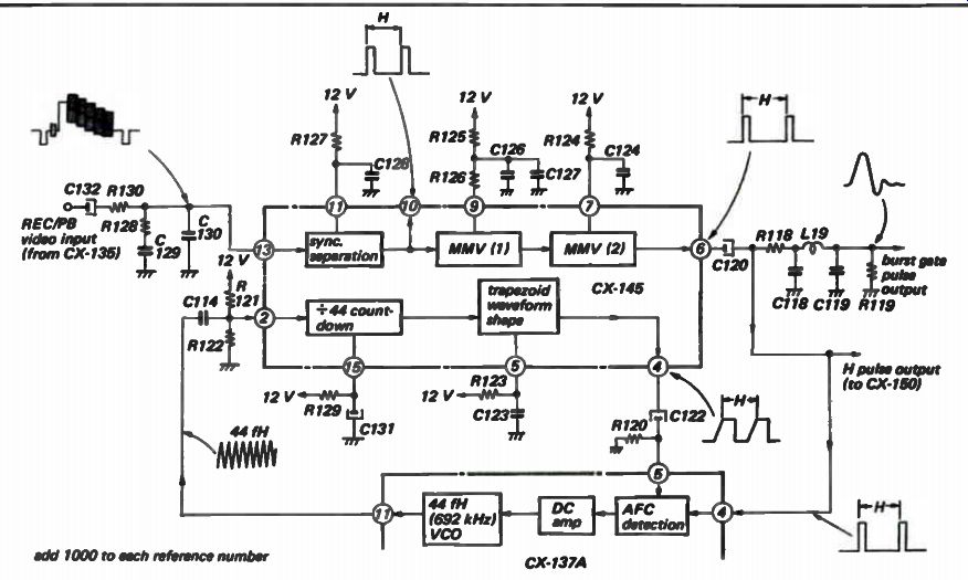
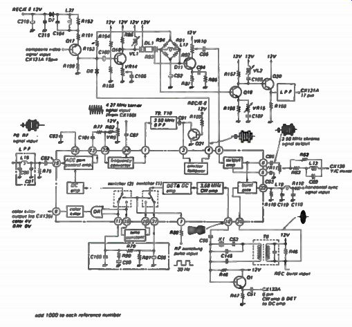
Fig. 8-4. Block diagram of the countdown circuits.
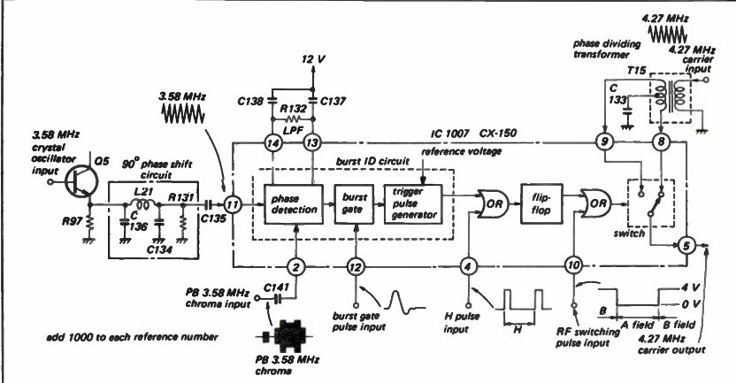
Fig. 8-5. IC 1007 chip block diagram.
The signal now passes through the 3.58-mHz filter and then to an emitter-follower circuit -pin 4 of IC 4-and is coupled to the comb filter, where the cross-talk component is removed. The comb filter output is fed to an output amplifier. From the amplifier, the signal is passed on to the Y/C mixer. The hobbyist in Fig. 8-3 is using the scope to check waveforms on the RS-L board.
Countdown Circuits
The sync separator, horizontal pulse generator and divide by-44 countdown circuit form a part of the afc loop. This circuit, shown in Fig. 8-4, is located on the YC-L board. The scope is used to check on operation of the multivibrator and the divide-by-44 countdown circuit.
Carrier Signal Phase Inverter and Burst ID Circuits
IC 1007, shown in Fig. 8-5, contains a carrier signal phase inverter circuit and a burst ID circuit. The carrier phase inverter consists of a flip-flop and switching circuit. A 4.27-MHz carrier signal is phase-split by the phase splitter transformer T15. The output from the secondary of T15 is fed to the switching circuit via pins 8 and 9. The normal phase 4.27-MHz carrier is fed to pin 8 and the out-of-phase carrier to pin 9. The dual-trace scope probes can be connected to pin 9 and 8 of IC 1007 to check on the 4.27-MHz signal and for a phase-shift from T15. The switching circuit is driven by the flip-flop output and the rf switching pulse, both of which are fed to the switcher through an OR gate. As shown in Fig. 8-5, the flip-flop is triggered by a horizontal pulse and toggles at a 1 horizontal rate. The output of this flip-flop and the 30-MHz rf switching pulse are applied to the OR gate. The output of the gate is waveform 7 in Fig. 8-6. The 4.27-MHz carrier output from pin 5 is fed to the chroma frequency converter circuits of the record and playback systems. Check with the scope at pin 5 for the 4.27-MHz signal to see if the IC switch is working properly.
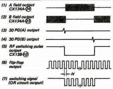
Fig. 8-6. OR gate waveforms.
The 688-MHz recorded chroma signal is phase-inverted line by-line on every track recorded by the A head. When this signal is recovered, it is necessary that the switching phase of the 4.27-MHz carrier is phase inverted line-by-line is the same as used in recording. Because the switching is done by a flip-flop toggled by a horizontal sync pulse, a signal loss caused by dropout would mean there is a good probability that the flip-flop would be in the wrong state at any given line of playback. To prevent this, a circuit is provided which determines the state of the flip-flop relative to the playback signal on a line-by-line basis and resets it if required. The circuit is a burst phase ID circuit that compares the phase of the playback burst signal against the 3.58-MHz stable crystal reference oscillator. Another scope check point would then be pin 11 of IC 1007 for the 3.58-MHz oscillator signal. This 3.58-MHz signal is a burst phase reference in the playback mode. When the apc loop is locked, there is a 90-degree phase difference between the playback burst signal from the reference oscillator. The output signal from the reference oscillator is fed through a 90-degree phase-shift network before it goes to the phase comparator. This places both the oscillator signal and the playback burst signal at the sane phase.
Whenever a phase inversion occurs between the two signals, because of mis-orientation of the flip-flop, a large output error signal is produced at the phase detector. This error signal pulse is fed to the flip-flop through the other input of the OR gate than that through which the flip-flop is normally toggled by the horizontal sync pulse.
It forces the flip-flop into the correct initial state.
Servo and Pulse Systems
The head servo system is operating while all of the video signal processing is taking place. Refer to Fig. 8-7 for a block diagram of servo circuits. The composite video input signal is fed to a sync separator which has the vertical sync pulses at its output. A second signal is fed to the servo circuits from the spinning disc of the video heads. This signal (called the PG or pulse generator pulse) is generated by a permanent magnet located on the video disc assembly which passes over a pickup coil as the heads rotate. The phase between the PG pulse and the vertical sync pulse is compared, and the speed of the head disc is varied until the two signals are in phase with each other.
The vertical signal is also fed to a stage that divides the frequency in half. This 30-Hz signal is fed to a recording head along the tape travel path. This head records the 30-Hz control track that will be used as a reference to control the servo circuits during playback.
The head drum is belt driven by an AC synchronous motor.
The drums free-running speed is set slightly higher than desired, and speed regulation is achieved by applying braking action. This brake is controlled by the servo system. The servo system controls the speed of the head drum only. The pulse system produces switching signals used in switching between the two heads and in switching the 4.27-MHz carrier. The position relationship of the video heads and the pulse generator coils (30 PG coils) is shown in Fig. 8-8.
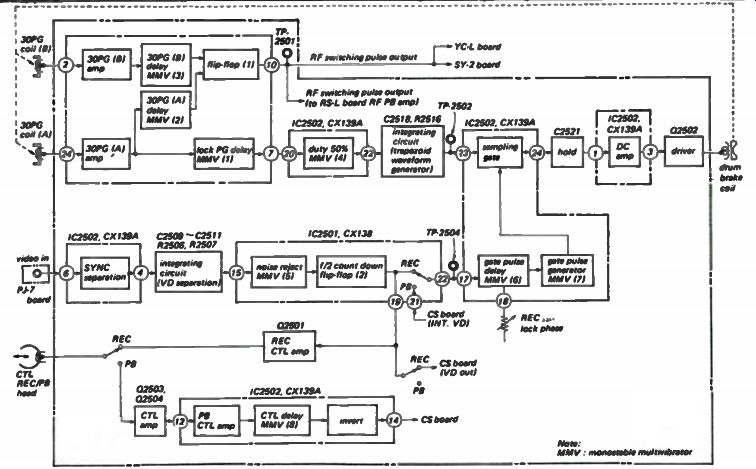
Fig. 8-7. Block diagram of servo circuits.
The two video heads are mounted 180 degrees apart on the periphery of the head disc. The magnetic pole pieces and PG coils are also mounted on the disc. The 30 PG (A) signal is used in the drum servo system, while the 30 PG (A and B) signals are used to produce the rf switching pulse. Use an oscilloscope to check for proper pulses from the PG coils.
The pulse generated by the 30 PG (A) coil is amplified by the 30 PG (A) amplifier and from there to both the lock PG delay multivibrator and delay MMV2. Both delay multivibrators are one-shot, toggled by the 30 PG (A) pulse, and both produce rectangular shaped output pulses. The output from MMV1 toggles a second one-shot, MMV4, which squares the signal into a 50-percent duty cycle waveform. The output from MMV4 is passed through an integrator network which converts the square-wave into a trapezoidal waveform. Use the scope to see if the pulses are being processed properly in the flip-flops and countdown chips found in the servo system.
The composite video is fed to the sync separator and then passed through an integrator network that removes only the vertical sync pulses. This is fed to a one-shot in the MMV5 which eliminates noise. The output from MMV5 toggles a flip-flop that divides and shapes the signal into a 30-MHz square wave. This signal is used in the record mode as the control (CTL) signal. It is also applied to a gate pulse to delay the one-shot MMV6, which in turn toggles MMV7, the gate pulse generator. The gate pulse is fed to the sample gate along with the trapezoidal 30 PG (A) signal. In the sample gate, the two signals are phase-compared, and the sample voltage is stored in a hold circuit. This stored voltage is amplified by DC amplifiers and controls the drum brake coil driver transistor. To lock up the servo on playback, a 300-Hz oscillator is phase-locked to the line frequency and counted down by a one-tenth countdown circuit which will form a 30-Hz square wave at test point 4604. This is a good scope test point to go to if you encounter servo problems.
This pulse is transferred to the tracking control circuit where it becomes the servo reference voltage during playback.
The servo control circuits of a video recorder simply compare two signals to indicate that the video heads are in the correct position during both recording and playback. During recording, the two signals are the vertical sync pulses and the head position signal (PG pulses). The two signals should arrive at the servo comparison circuits at the same time. A dual-trace scope is a must for evaluating this action. If they are not properly timed, the servo circuits will adjust the rotational speed of the video heads until the two signals correspond.
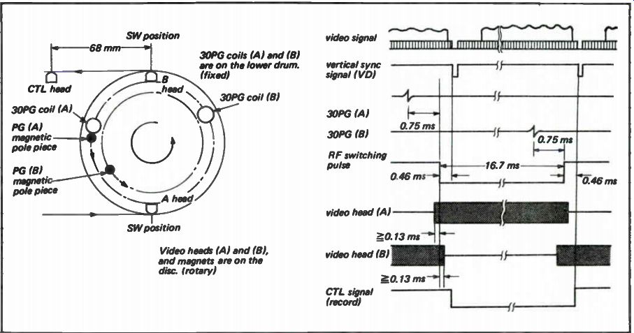
Fig. 8-8. Relationship between heads and PG coils.
During playback, the same head reference pulse (PG pulse) is compared with the output of the control track head. Again, the two signals are compared and the speed of the rotating head disc is adjusted until the two pulses are properly timed. Signal pulse injection may also be used to analyze some sections of the servo circuits that are difficult to analyze using the scope or other troubleshooting techniques.
Signal injection works very well when combined with an oscilloscope for signal tracing. Just inject the subber signal at the input to a stage and monitor the resulting signal at the output of the same stage or one that is supposed to be controlled by the injected signal.
Many circuits in the VCR require that both the amplitude and the waveshape of the signals be correct. In these cases, the use of an oscilloscope is essential. The combination of both signal tracing and signal injection in many cases provides the best analyzing techniques.
Servo Timing and Generating Circuits
The vertical sync signals, separated from the video input signal, becomes the servo reference signal in the record mode.
Note the block diagram shown in Fig. 8-9. The filter rejects the chroma burst signal and high frequency noise. The video output is connected as an input to the RS-L board. If you have servo and timing trouble, check with a scope and see if you are getting the proper video signal input at this point.
The video signal is sync-separated in the circuit between pins 6 and 4 of IC 502. The sync separation circuit consists of a feedback clamp circuit for sag correction and a switching amplifier. An RC integrator circuit separates the vertical sync from the sync separator output and triggers the noise elimination one-shot, MMV 5, via SW (1) of IC 501. SW (1) switches to the pin 15 side for a zero-volt input at pin 16 and to the pin 14 side for 12 volts. The noise elimination one-shot, MMV(5), eliminates noise by the fact that a one-shot, once toggled, cannot be toggled again until after it has reset itself. The external circuit at pin 17 is the time constant network for MMV 5. The 60-Hz vertical signal is divided into a 30-Hz square wave in the divide-by-two flip-flop. The 30-Hz square wave passes through SW (3) and appears as the gate signal output at pin 22.
The negative-going transition of the flip-flop output becomes the servo reference phase that is used on the video tape control track. The proper phasing of the integrated pulse will appear at pin 9 of IC 502. Thus, the internal vertical reference signal becomes the gate signal for control of the drum servo.
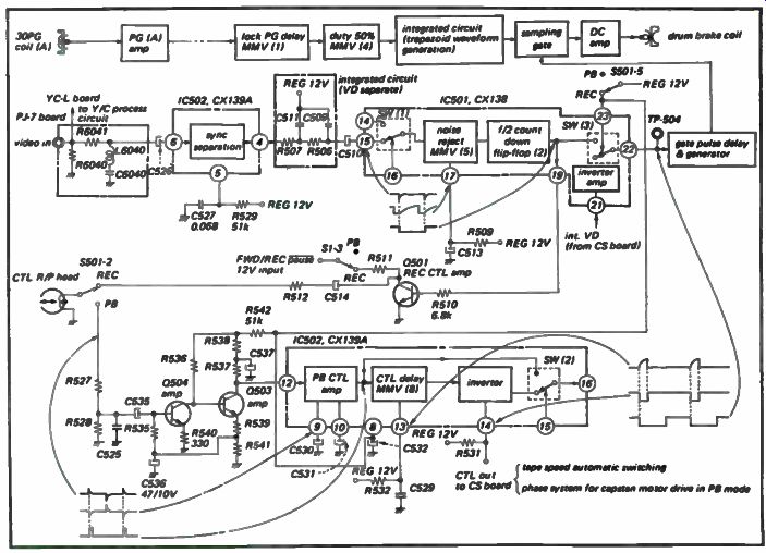
Fig. 8-9. Vertical sync and CTL signal circuits.
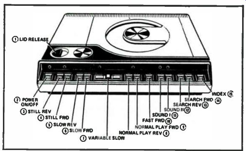
Fig. 8-10. Front panel view of the Magnavox Videodisc player.
THE MAGNAVOX MODEL VH 8000 VIDEO PLAYER
In this section we will look at some of the many new circuits found in the Magnavox Videodisc player. This unit uses a laser beam to recover video and audio information from a disc to produce high quality pictures and sound on any color TV receiver. The front panel view of the VH 8000 is shown in Fig. 8-10.
Servo Controls
The servo control circuitry performs the following functions in the videodisc machine.
• Turntable motor control.
• Tangential tracking mirror control.
• Radial tracking mirror control.
• Slide drive control.
• Objective lens control (focus).
• Turn-on sequence logic.
The turntable motor control and the tangential mirror control operate together. Their purpose is to keep the track movement over the light beam at a constant velocity. Refer to Fig. 8-11 for the complete laser optical path. Errors in the velocity of the track over the beam become timing errors in the video signal. Speed errors can be caused by an unstable turntable motor speed or eccentric rotation caused by an off-centered hole. An inherent 30-Hz error exists due to the eccentricity of the tracks. They are actually a spiral instead of perfect circles.
Correct motor speed is maintained by comparing the horizontal video sync pulses with a locally generated crystal-controlled oscillator. However, even with correct motor speed, instantaneous speed errors occur as the track travels an eccentric path. These speed errors occur at a 30-Hz rate (the speed of a standard play disc). The 30-Hz eccentricity errors and other momentary speed variations are corrected by controlling the moveable tangential mirror.
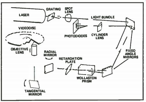
Fig. 8-11. Optical path drawing.
The block diagram in Fig. 8-12 shows the arrangement used to compensate for time errors. A locally generated 15,734-Hz oscillator is used as a master reference. The composite video signal serves as an indicator of the disc speed. If the disc is too fast, the sync pulses will be too close together. Slower than normal speed causes the sync pulses to be farther apart.
The turntable motor cannot change speed instantaneously, so it responds only to gradual speed errors. The tangential mirror, however, can move very quickly. It responds to the higher frequency errors, such as the 30-Hz speed changes. An electronic tangential loop switch is used to take the tangential mirror out of the circuit whenever the turntable motor is not at the correct speed.
A sync separator strips the sync from the composite video signal and feeds negative-going composite sync to the filtered sync generator. This generator simply generates a new sync pulse with the same frequency as the original, but with filtering added during the time between sync pulses. In this manner, no unwanted spikes between sync pulses can upset circuit operation.
The filtered sync is fed to the motor phase detector along with a pulse from the reference oscillator. The output of the motor phase detector is fed to the motor drive servo that spins the turntable motor. If the phase of the filtered sync should ever drift with respect to the reference pulse, the motor phase detector will cause the motor drive servo to correct the motor speed.
Another output from the motor phase detector is used to control the electronic tangential loopswitch. If the sync frequency is not equal to the reference frequency, the tangential loopswitch is opened, taking the tangential mirror out of the circuit. The mirror will remain inactive until such time as the motor resumes its correct speed.
The composite video signal is also used to create a reference for the tangential mirror control. However, the sync pulse cannot be used because its leading edge is not precise enough. Therefore, a sample pulse is generated, using the burst as a precise reference.
The composite signal is applied to the burst 0 cross detector.
This detector creates a pulse each time the sinusoidal burst signal passes through zero. The result is a 7.16-MHz chain of very accurate timing pulses during the burst time. These are applied to the sample pulse generator. The generator creates the sample pulse which begins at the same time as one of the zero cross burst pulses. The same zero cross pulse always triggers the sample pulse on each horizontal line. The sample pulse thus becomes a very precise reference for the horizontal frequency of the composite video signal.
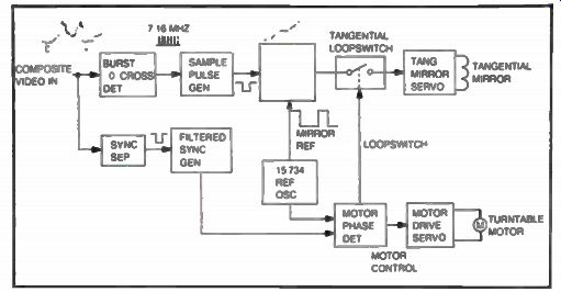
Fig. 8-12. Block diagram of tangential and motor drive.
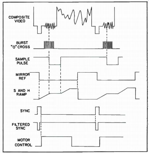
Fig. 8-13. Tangential and motor drive control signals.
The sample pulse and the mirror reference pulse from the reference oscillator are both fed to the sample and hold tangential phase detector. The mirror reference pulse starts a ramp voltage during every horizontal line. When the sample pulse is present, the ramp is stopped and a sample is taken off the ramp voltage at that point. Any phase shift in the sample pulse (indicating a speed change) will cause the sample to be taken at a higher or lower point on the ramp. The sample voltage is stored and becomes the correction voltage applied to the tangential mirror servo through the closed loopswitch. Because the sample pulse and ramp occur at the horizontal rate, the correction voltage is updated 15,734 times per second. The largest component of correction occurs at a 30-Hz rate because of the elliptical tracks and the 30-Hz speed of the videodisc.
The timing waveforms and their relationship to each other are shown in Fig. 8-13.
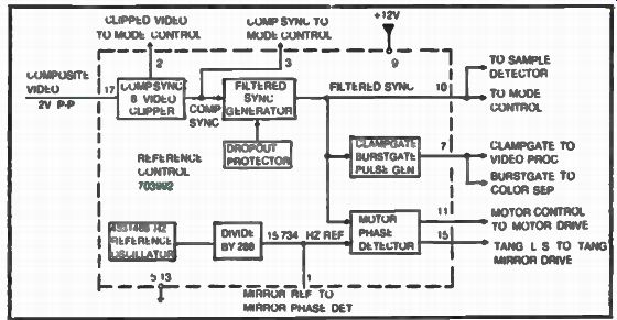
Fig. 8-14. Reference control module circuit.
Reference Control Module Circuit
The block diagram shown in Fig. 8-14 is of the reference control module. The composite video signal input at pin 17 is fed to the composite sync and video clipper. This circuit clips the video signal at two different levels. One clipper creates the clipped video signal, which is sent out pin 2 to the mode control module. The mode control module samples this output only at the proper times to retrieve the digital code information for the picture number.
Another clipper removes the composite sync and feeds it to the mode control module at pin 3 and to a filtered sync generator. The mode control module uses the composite sync signal to generate timing pulses to place the picture number in the upper left-hand corner of the screen. The filtered sync generator merely regenerates a new sync signal with the same frequency as the original but with filtering added during the time between pulses. In case of faulty sync from a dropout, a dropout protector will reinsert a new sync signal to replace the missing one. The filtered sync exits the module at pin 10 and is also applied simultaneously to the clamp gate and burst gate pulse generator and to one input of the motor phase detector. The clamp gate pulse is used to clamp the video to the correct DC level on the video processor module. It also gates the burst out of the video on the color separator module.
The other input to the motor phase detector is the 15,734-Hz reference signal. This signal is derived from a 4.53-MHz reference oscillator that is divided down to obtain the 15,734-Hz reference frequency. These two inputs are compared in the motor phase detector and develop the motor control signal at pin 11 and the tangential loop switch voltage at pin 15. The 15,734-Hz reference signal at pin 1 is also used as the mirror phase detector module.
Drive and Track Control Logic Circuits
The block diagram in Fig. 8-15 shows the radial drive and track jump logic circuits. During normal play, the high-frequency compensated radial error signal from the preamp module is fed to an error amp on the radial drive module. This stage is gain-controlled by R3002. The error signal is coupled through the closed radial loop switch to a complementary type power amp which drives the radial mirror. The radial drive module also has the radial limit circuit. This circuit sets the maximum allowable tilt of the radial mirror and is adjustable by R3026. Should this limit be reached, the radial limit circuit will open the loop switch and allow the mirror to fall back to its center position.
The trick logic, search adaptor and mode control modules are only used during special modes of operation. An input from the front panel buttons is sent to the mode control module. Immediately after vertical sync, the track jump logic generates P2 simultaneously with P1 or PIA. The sequence at which Pl and KA are generated depends on the particular mode of operation.
The true radial error signal from the preamp is sent to a zero cross detector on the track logic module. This detector creates an output each time the radial signal passes through zero. The zero cross signal is compared with the vertical sync serrations in the zero cross logic to develop a zero detect signal. This signal is used by the track jump logic on the mode control module to switch from P1 to PIA, or vice versa.
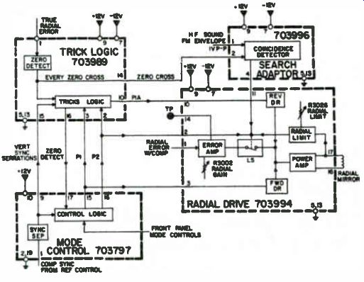
Fig. 8-15. Radial drive and track jump logic circuits.
--------------------