AMAZON multi-meters discounts AMAZON oscilloscope discounts
The process of miniaturizing multi-device circuits (transistors, resistors, diodes, etc.) is called integration. An integrated circuit (IC) is a chip that contains (or can perform the function of) many discrete (nonintegrated) devices.
In appearance, most common types of ICs are small, rectangular packages with 8 to 16 pins (or legs) extending from the package. This physical configuration is called a dual in-line package (DIP). Other common package styles include round metal casings with multiple leads extending from them, and larger rectangular packages with up to 40 pins.
Most ICs are manufactured as general-purpose building blocks with in a specific functional area. For example, the common 741 operational amplifier is designed specifically for amplification type functions, but its external component design can modify its performance for literally thousands of different applications. In contrast, many ICs are manufactured for very specific applications, especially in the consumer electronics field. For example, an IC specified for use as a rotational speed control for VCR heads can be used for little else.
It is easy to integrate semiconductor components (or components that can be made from semiconductor materials). Very large-scale integration (VLSI) chips can contain as many as 250,000 transistors. Resistors can be made very accurately from semiconductor material. However, large-value "reactive" components, such as inductors and capacitors, cannot be reduced in size. Also, semiconductor components designed to dissipate large quantities of power cannot be integrated very successfully. For these reasons, many ICs are nothing more than the total low-power semiconductor part of a larger circuit. The reactive and high-power components must be added for a functioning circuit. "Switching regulator control" ICs are a good example of this kind of design.
Because of the vast number of integrated circuits available, it is absolutely necessary to have a good selection of manufacturers' data books in your electronics library. You will have to depend on these data books to obtain pin-out diagrams (illustrations of the functional aspects of each connection lead on an IC), application information, and functional specifications.
ICs can be divided into two main families: digital and linear (or analog). Digital ICs will be discussed in the next section, so in this section, we will concentrate primarily on linear devices.
Linear ICs can be further subdivided into several classifications: operational amplifiers, audio amplifiers, voltage regulators, and special purpose devices.
For very common applications, a manufacturer may build a complete circuit, using ICs and discrete components, and encapsulate the complete circuit into a block. These devices are called hybrid modules . Common hybrid modules include high-power audio amplifiers, power supply regulators, motor controls, and certain types of high-power, high-voltage devices.
Operational Amplifiers
Operational amplifiers are basic amplification building blocks. They consist of multiple high-gain differential amplifiers (exhibiting high common-mode rejection) without any kind of feedback loop. Depending on the configuration of the external components, they can be used for voltage amplifiers, transconductance amplifiers (voltage-to-current converters), transimpedance amplifiers (current-to-voltage converters), differentiators, integrators, comparators, oscillators, and regulators.
Virtually all operational amplifiers ("op amps") have two inputs marked with a positive (+) sign and negative (-) sign. These are the non-inverting inputs and inverting inputs, respectively. Don't confuse these with the power supply connections. Many op amps have frequency compensation inputs. Normally, a capacitor or resistor-capacitor combi nation is connected between these pins for controlling high-frequency characteristics. Offset null inputs are provided on many op amps to bias the output at a desired DC quiescent level.
Op amps are not specified in regard to frequency response, because it will vary depending on the way the op amp is used in a circuit. For example, an opamp used as a voltage amplifier (with the external components setting its gain at 10) will have a much broader frequency response than if the external components set its gain at 1000. Therefore, the frequency response characteristic of op amps is defined by the term slew rate, which is the speed (given in microseconds or nanoseconds) in an op amp's output change in accordance with an instantaneous change on the inputs. The higher the slew rate, the higher the maximum usable frequency response.
Most op amps are designed for use with dual-polarity power supplies. The power supply voltages should be equal, but opposite in polarity. Opamps designed for dual-polarity power supplies can work with single polarity supplies for certain applications. Also, some op amps are designed exclusively for single-polarity supplies.
The "perfect" opamp would have infinite gain, zero output impedance, infinite input impedance, and instantaneous slew rate, and be totally immune to common-mode noise on the power supply inputs and signal voltage inputs. If a perfect op amp existed, the circuit designer could use external components to design any feasible type of op amp circuit without any consideration of op amp parameters or limitations.
Of course, perfection is not possible, but modern op amps, especially "FET input" op amps, come close to perfection parameters. Therefore, the equations used for designing amplifiers, filters, oscillators, and other circuits, seldom include any op amp variables.
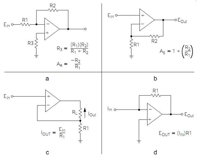
FIG. 1 Common op amp circuit configurations.
FIG. 1 illustrates some examples of common op amp circuit con figurations. These illustrations do not give pin numbers or power supply connections because they are general in nature. Virtually any general-purpose op amp will work in these circuits, and many high-quality, low-noise op amps will work better. For these circuits, and almost any type of op amp circuit, I highly recommend the low-noise NE5532 (NTE778A) dual op amp ICs, although the industry-standard 741 type will probably perform satisfactorily in most cases. For critical audio circuits (preamplifiers, mixers, tone controls, etc.), I recommend the TL-074 op amps, which boast a high slew rate and 0.005% THD (total harmonic distortion).
Referring again to FIG. 1, examine some details of each circuit illustrated. Circuit A is an inverting voltage amplifier. The equation for calculating voltage gain shows that it is solely dependent on the ratio of R1 and R2. For example, if R1 is 10 Kohm and R2 is 100 Kohm, the voltage gain is 10. The negative sign (-) is placed in front of the R1/R2 ratio expression to show that the output will be inverted. R2 in this circuit is the negative feedback resistor. Note that it is connected from the inverting input to the output. The output portion being "feedback" to the input will be inverted, or opposing in nature. Consequently, it is negative feedback. R3 is used for circuit stabilization, and its calculation is included in the illustration.
Circuit B is a noninverting voltage amplifier and, as the gain equation shows, its gain is also dependent on the ratio of R1 and R2.
Circuit C is a transconductance amplifier, or a voltage-to-current converter. The current output, which is the current flow through RL , will not be dependent on the resistance value of RL. Rather, it will be dependent on the ratio of the input voltage to the value of R1.
Circuit D is a transimpedance amplifier, which functions in a manner opposite to that of circuit C. Circuit D converts an input current into a proportional voltage. The associated equation for this function defines the component relationship.
All of the circuits illustrated in FIG. 1 must be designed with their power supply limitations in mind. For example, circuit A cannot be designed so that a desired input and voltage gain will drive the output in excess of the power supply voltages used. In the same way, the manufacturer's specified maximum power dissipation cannot be exceeded with out destroying the chip. In multiple op amp circuit designs, it may also be necessary to decouple the individual op amp circuits (usually with about a 100-uF electrolytic capacitor and a 0.1-uF nonpolarized capacitor).
IC or Hybrid Audio Amplifiers
Many currently available audio amplifiers are offered as "totally integrated" or hybrid. To the electronic "user," the only major difference is in reference to size; hybrid circuits are typically larger, and might require a larger heatsink.
In general, audio amplifier ICs might be thought of as "simple-to-use power op amps," because that is essentially what they are. Many types are designed for single-polarity power supplies (which make them excellent for battery-powered applications), and they frequently have internal gain and frequency compensation networks. These attributes, together with others, add up to a quick and simple, general-purpose audio amplification system for low- to medium-power applications. Heatsinks are typically required for outputs in excess of 1 watt.
Although great progress has been made in the integration techniques of audio amplifiers, the performance levels of many medium to high power systems leaves much to be desired. For this reason, most audiophiles still prefer discrete audio power amplifiers in the majority of cases.
IC Voltage Regulators
This is an area where ICs have virtually taken over. Typical IC voltage regulators provide almost unexcelled voltage regulation, overvoltage protection, current limiting, and automatic thermal shutdown (the unit shuts off when it gets too hot), and many are adjustable. In addition, they are commonly available and very inexpensive. It's no wonder they are popular.
In addition to all of their other desirable attributes, voltage regulator ICs are very easy to use and implement for almost any application. Most have only three connection terminals; one is the "raw" DC input, another is the output, and the third simply connects to circuit common, or to a single potentiometer for voltage adjustment. You can't get much simpler than that! The small size and low cost of regulator ICs has made it practical to use them as onboard regulators for each individual printed circuit board within an entire system. This has reduced the need (and cost) of large, high-current regulated power supplies for larger electronic systems. And, because this puts them in close proximity to each PC board within a system, the regulation and noise immunity is usually better than can be achieved with a large central power supply.
Regulator ICs commonly require heatsinking for maximum output.
Most are available in either TO-220 or TO-3 packages. This causes them to look like power transistors, but it provides them the flexibility to be mounted on the many styles of transistor heatsinks already available.
Special-Purpose ICs
There are many more special-purpose integrated circuits than there are pages in this guide. The determining factor as to whether any particular circuit will be available in IC form is purely economic. It is expensive for a manufacturer to do the research and development (R&D) required to produce a new type of IC. Consequently, manufacturers do extensive marketing research (to ensure the demand, in great quantities, for a special-purpose IC) before they can justify the cost of the initial investment. If they do not believe that they can regain their R&D costs, the IC is not manufactured.
Skim through several IC data books to acquire a basic knowledge of "what's out there" regarding special-purpose ICs. Before using a special purpose IC, closely examine its specifications. There are many examples where discrete versions of circuits will perform better than their IC counterparts.
Improvement of Lab-Quality Power Supply
The lab-quality power supply, as discussed in Sections 3 through 6 of this guide, has a minor shortcoming. If you have used this supply for many of the prior projects, you might have noticed that the output voltage will drop slightly when the supply is heavily loaded. Because this power supply was offered as the first project in this guide, I felt it was prudent to keep the parts count and complexity to a minimum.
Although many commercial power supplies utilize this same basic design, it might not measure up to some of your future requirements in more critical circuits. Therefore, this section will detail two ways of improving the voltage regulation performance; it's up to you to decide on either method. You might also decide to leave this supply as it is, and build the quad power supply detailed in the next section instead.
First, refer back to Fig. 11 in Section 6. To improve the voltage regulation of this circuit, it is necessary to increase the gain of the Q3 and Q4 stages. One method of increasing gain would be to replace Q3 and Q4 with Darlington pairs. Another method, providing even tighter control, is illustrated in FIG. 2.
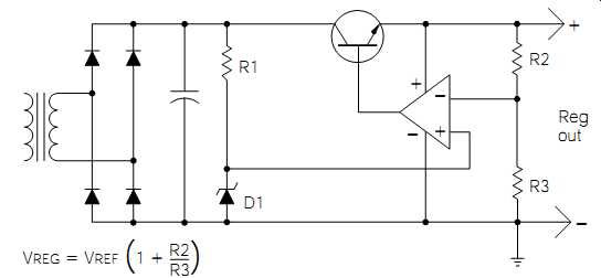
FIG. 2--Improvement of lab quality power supply.
Although the circuit in FIG. 2 shows only the positive regulator, you would simply duplicate the basic theory and design in the negative regulator. (The current-limiting circuit of Sect. 6, Fig. 11 is not shown in FIG. 2 for the sake of clarity.) Q3 of Fig. 11 would be replaced by the general purpose op amp shown in FIG. 2. The inverting input of the op amp would connect to the wiper of the voltage control potentiometer, P1, and the noninverting input would connect to the anode of D1 (the voltage reference diodes in Fig. 11). The output of the op amp connects to the base of Q1 (the series-pass transistor, Fig. 11), and the op amp power supply connections are made to the positive and circuit common points as illustrated.
The circuit, shown in FIG. 2, is included as a basic reference for all of your future power supply needs. To use this design, start by designing a simple zener-regulated power supply (the transformer, bridge rectifier, filter capacitor, R1, and D1). Be sure that the zener voltage of D1 is somewhat less than the anticipated voltage drop across R3. The equation for calculating the value of R2 and R3 is provided in the illustration. Of course, Q1 is chosen according to the current and power dissipation requirements of the proposed loads to be applied to the circuit.
The best method of improving the lab power supply is illustrated in FIG. 3. The full regulator circuit design has been included so that the circuit modifications might be more easily located. These alterations should be self-explanatory by comparing Fig. 11 with FIG. 3. Note that you will need to mount two additional binding posts for the positive and negative regulated outputs. Keep the original two posts intact, connected to the unregulated current limit circuit, for testing audio power amplifiers (and other projects requiring higher-voltage, dual polarity supplies). Also note that P1 and P2 must be replaced with 5-Kohm potentiometers.
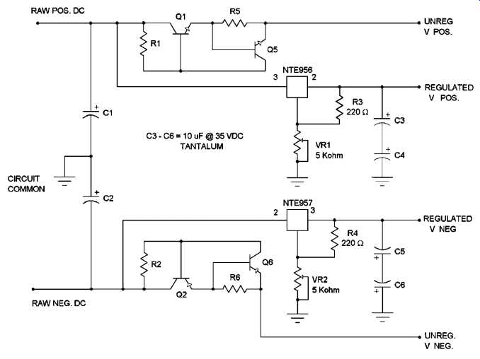
FIG. 3 Improvement of original lab power supply illustrated in Fig.
11 ,Sec. 6.
Building a Quad Power Supply
FIG. 4 illustrates a quad-output lab power supply. This is an extremely versatile lab power supply. It provides the most frequently used voltages in dual polarity. Each output is current-limited at 1.5 amps, and all of the regulator ICs are internally protected from overvoltage and overtemperature conditions. The regulator ICs are of the fixed-voltage type, meaning that they are not voltage-adjustable, but they provide extremely good voltage regulation. All of the power supply components have been chosen so that all four outputs can be loaded to maximum capacity simultaneously.
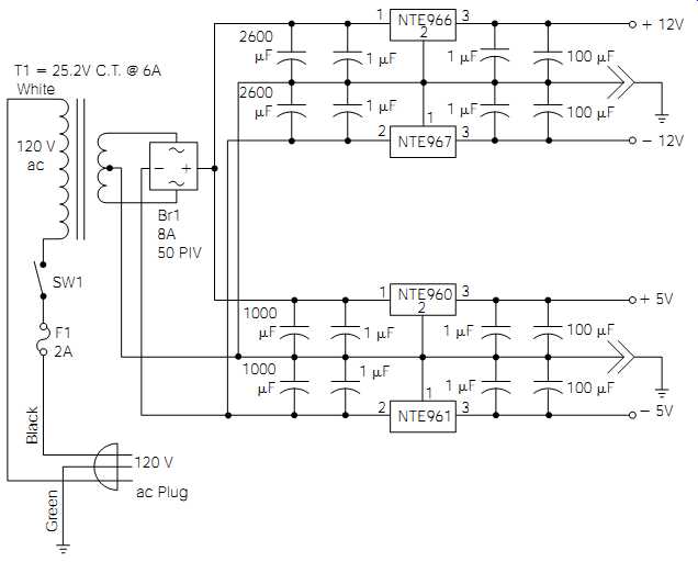
FIG. 4--A quad-output lab power supply.
All four regulator ICs will require some form of heatsinking. Mounting the ICs to a metal enclosure will probably be sufficient, but the combination of the chassis and the "sinks" is recommended. After constructing the power supply, load down all four outputs, and let it run for a while. If the enclosure (or the ICs) start to become too hot, you will need to include some additional heatsinking between the enclosure and IC mounting tabs.
Circuit Projects
Noise Hangs in the Balance
Most high-quality microphones, those designed for professional entertainment use, are low-impedance devices and have balanced XLR-type connector outputs. Although these "mikes" can be impedance matched for a high-impedance input with a single transistor stage, this will defeat the whole purpose of having a balanced line.
The circuit illustrated in FIG. 5 will match the impedance correctly, and utilize the high common-mode rejection characteristic of operational amplifiers to remove the unwanted "hum" picked up by long microphone wires.
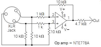
FIG. 5 A balanced input circuit for low-impedance microphones.
Hum Reducer
Furthermore, on the subject of hum (stray 60-hertz noise, inductively coupled to an audio circuit), the circuit illustrated in FIG. 6 can do a very effective job of removing almost all hum content, even after it has already been mixed with other audio material. However, it will also reduce some low-bass frequencies (from about 40 to 100 hertz).
FIG. 6 shows a "twin-tee" notch filter. The component values chosen will cause the output to drastically attenuate 60-hertz frequencies, but allow most other frequencies to pass unaltered. Attenuation at 60 hertz should be on the order of about 12 dB.
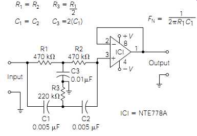
FIG. 6 A 60-hertz notch filter.
Equations are provided in the illustration to design notch filters for other frequencies, also. Notice the equation for finding the notch frequency (FN). The little symbol with the two legs and a wavy top is called pi. Pi is a mathematical standard, and it is approximately equal to 3.1416.
Bandpass
FIG. 7 is an example of a bandpass filter. A bandpass filter only passes a narrow band of frequencies, and severely attenuates all others. This circuit illustrates how a JFET can be used as a voltage-controlled resistor; to "tune" the bandpass frequencies of the filter by means of a control voltage (about 0 to 2 volts DC). The usable frequency range is from sub-audio to about 3 kHz. This circuit is commonly used to produce "wah-wah" effects for electric guitars and other instruments.
When several of these circuits are placed in parallel with component values chosen to provide different ranges of bandpass, the result is a parametric filter. If a manual control of the bandpass is desired, Q1 might be replaced with a 5-Kohm resistor.
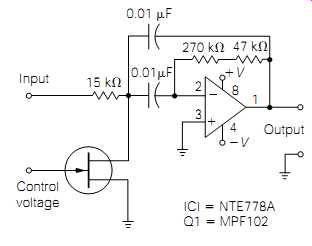
FIG. 7 A voltage-controlled bandpass filter.
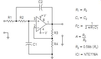
FIG. 8 Low-pass filter.
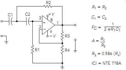
FIG. 9 High-pass filter.
High-Versatility Filters
Figures 12-8 and 12-9 are both examples of equal-component, Sallen-Key active filter circuits. Equal-component filters are easier to build, because other filter designs require exact multiples or divisions of the values of key components which might not be standard in value. FIG. 8 is a low-pass filter, and FIG. 9 is a high-pass design. Both designs provide about 12 dB-per octave of signal attenuation (rolloff) for the unwanted frequencies.
To design these filter circuits for your own applications, start with R3 =_ 12 K-ohms and R4 = 22 K-ohms. Using R1 and R2 values of 4.7 K-ohms, and C1 and C2 values of 0.005 uF, Fc should be a little over 6 kHz. From this point, you can adjust component values, as needed, by following the equations provided in the illustrations.
These circuits can be cascaded (in series) for sharper cutoff responses.
For example, if two FIG. 8 circuits were built, each having a cutoff frequency of 6 kHz, and they were placed in series, the final output would have a 24-dB/octave rolloff. The FIG. 8 and FIG. 9 circuits can also be placed in series to provide precise bandpass responses with both upper and lower cutoff frequencies. For example, assume that you need a filter circuit to reject all frequencies except those occurring between 6 and 8 kHz. You would design the low-pass filter for a cutoff frequency of 8 kHz, and the high-pass filter for a cutoff of 6 kHz. By placing the two filter circuits in series, the total response would be that of a bandpass filter with a "passband" of 6 to 8 kHz.
Trip-Point Relay
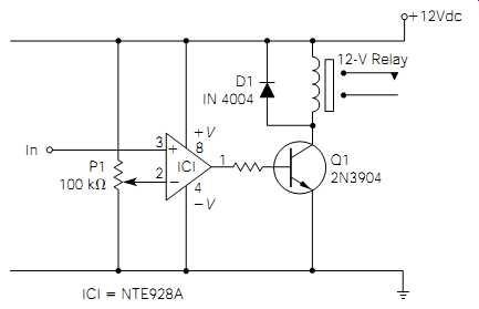
FIG. 10 Adjustable trip-point relay driver.
FIG. 10 illustrates an adjustable trip-point relay driver. This is an example of how an operational amplifier can be used as a "comparator." A comparator circuit "compares" two voltages. When one exceeds the other, a signal is provided.
The op amp compares an adjustable reference voltage, provided by P1, to an input voltage. When the input voltage exceeds the reference voltage, the op amp output goes high, turning on Q1, which energizes the relay.
The relay, of course, can be used to turn on, or provide power to, just about any kind of device. For precise, repeatable performance, the positive rail should be regulated by an LM7812 (NTE966) positive voltage regulator.
Circuits of this nature are used primarily for control applications. For example, different variables such as temperature, humidity, or light could be utilized to control other circuits, appliances, or machinery. For a security light controller, a photoresistor and fixed resistor, in series as a voltage-divider network, could be connected between the positive rail and ground. The input to the op amp could be connected to the junction between the two. If this circuit were to be placed outdoors, the resistance of the photoresistor would increase as the sun started to set. When the voltage drop across the photoresistor became high enough to exceed the reference voltage applied to the op amp, the relay would be energized turning on an outside light.
When two op amps are configured as comparators, one referenced to a low voltage and the other to a higher voltage (called high and low trip points), the resulting circuit is called a window comparator. Window comparators are used to control a variable within a set of operating parameters.
Watt an Amplifier
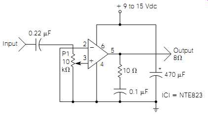
FIG. 11--A 1-watt audio amplifier.
The simple circuit of FIG. 11 is a 1-watt IC audio amplifier. P1 is the volume control. The rest of the circuit is self-explanatory.
This circuit works very well in battery-powered applications, and makes an excellent little amplifier for many of the sound-effect circuits covered previously in this guide.
Control Your Tone
As a final entry into this section of circuit Projects, I submit the easy to-construct and extremely versatile tone control and preamplifier combination illustrated in FIG. 12. I've also added some additional circuitry to illustrate an optional method of incorporating this circuit into almost any high-quality audio power amplifier system.
Starting at the left side of the illustration, IC1 and its associated circuitry constitute a typical inverting amplifier, identical to the amplifier circuit illustrated in FIG. 1, circuit A. As you will note, the ratio of the feedback resistor (47 Kohm) to the input resistor (4.7 Kohm) is 10:1, so the voltage gain is set at 10. However, you can change this ratio for more or less gain, according to your needs. The 100-pF capacitor across the audio input connections is for filtering out any unwanted high-frequency (HF) interference signals that may be present on the audio input signal.
The output of IC1 is connected to a 100-Kohm potentiometer that allows you to "tap off" any percentage of the amplified audio signal desired. In other words, it is your "volume" control.
From the tap of the volume potentiometer, the audio signal must pass through a system of RC filters, similar to the tone control circuit illustrated in Fig. 7 of Section 8. Note that the inverting input of IC2 is coming from the filter network. If you follow the output of IC2 to the junction of the two 5.6-Kohm resistors, you'll note that the output connects back into the filter network. In other words, the filter net work actually makes up the negative-feedback path for IC2 (i.e., the output of IC2 connects to the filter network, and the output signal is fed back to the inverting input of IC2 through the filter network). There fore, this circuit is an "active" tone control circuit, and it provides very good performance.
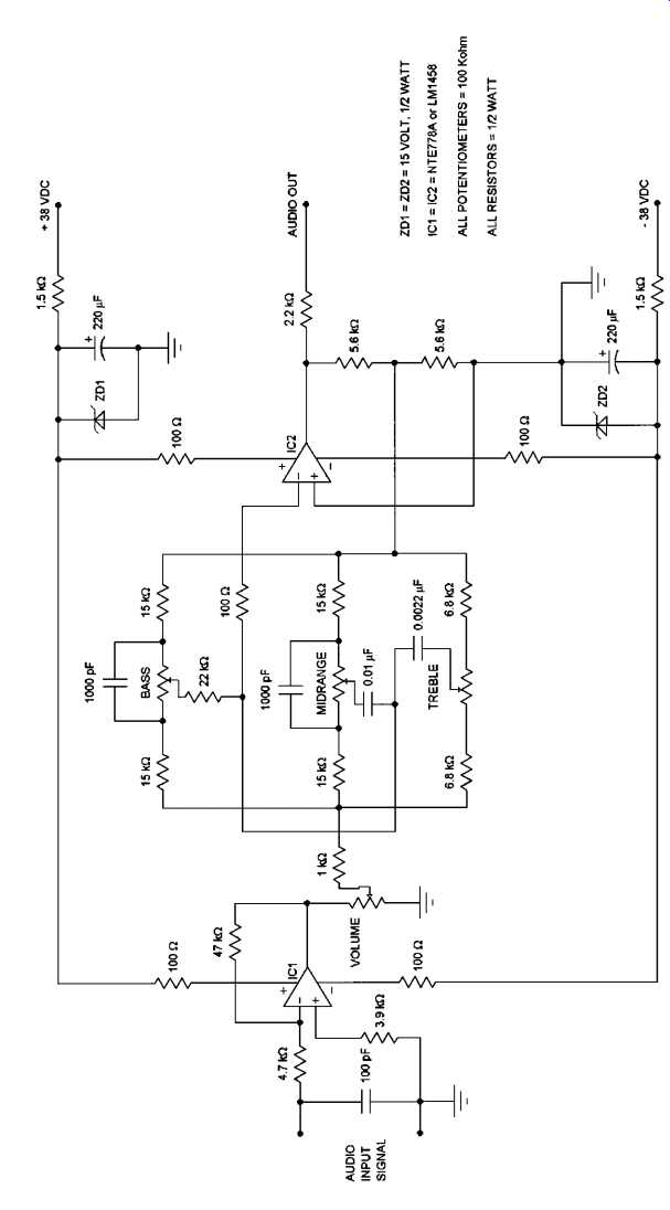
FIG. 12--General-purpose preamplifier and tone control circuit.
You will notice that the operational power for the op amps is obtained from two zener-regulated power supplies connected to a dual polarity 38-volt DC power supply. The zener diodes are 15-volt, 1/2-watt units, so the voltage at the cathode of ZD1 is approximately 15 volts DC, and the voltage at the anode of ZD2 is approximately 15 volts DC. The two 1.5-Kohm resistors in series with the zeners are the "dropping" resistors. This power supply configuration shows how this circuit can be connected directly to "rail" power supplies of typical audio power amplifiers. For rail voltages higher or lower than 38 volts, the value of the series dropping resistors would have to be changed accordingly. Naturally, if you wanted to provide operational power to this circuit with typical dual-polarity 12- or 15-volt supplies, you would simply omit the two zener diodes and their associated components (i.e., the 1.5-Kohm drop ping resistors and 220-uF filter capacitors).
LM1458 or NTE778A operational amplifiers are specified for this circuit, but almost any general-purpose op amp will provide satisfactory results. If you want to significantly improve performance for a high quality application, you could use TL-074, OP-176, or AD797 operational amplifiers. In addition to utilizing high-performance operational amplifiers, the signal-to-noise ratio (SNR) can be improved by using 1% metal film resistors instead of the more common carbon film or carbon composition types of resistors.