AMAZON multi-meters discounts AMAZON oscilloscope discounts
In a general sense, the entire massive field of electronics can be classified into two very broad categories: digital and linear. Digital pertains to those circuits and devices that operate on the basis of switching action, representing numbers or data by means of on-off pulses. The fundamentals of digital electronics will be covered in later sections.
In this section, you will examine the fundamentals of linear circuits. The term linear pertains to circuits that operate in a proportional manner, accepting inputs and providing outputs that are continuously variable (i.e., analog).
Although the field of linear electronics is very diversified, the basics of linear action are common to almost all of its facets. For example, the same techniques used to linearize (i.e., increase proportional accuracy in) an audio amplifier are used to linearize servo systems and operational amplifiers. An accurate understanding of the basic building blocks utilized in linear systems will aid you in understanding a great variety of electronic systems.
Because of a variety of factors, "discrete" (i.e., nonintegrated) circuitry is still utilized in a significant portion of the field of audio electronics. Therefore, this section focuses primarily on audio amplification circuits, since they provide a good beginning point to study the fundamentals of linear circuitry. In addition, the associative discussions make it a convenient point to detail printed circuit board construction (in conjunction with a few more "advanced" projects) and the newer computer-automated (also -aided or -assisted) design (CAD) techniques for designing and constructing PC boards.
Transistor Biasing and Load Considerations
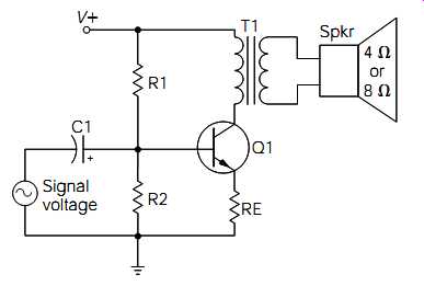
FIG. 1 Basic audio amplifier circuit.
The circuit illustrated in FIG. 1 should already be familiar to you from the previous discussions of transistor amplifiers. It is a common-emitter amplifier because the output (to the speaker) is taken off from the collector, and the input signal to be amplified is coupled to the base. C1 is a coupling capacitor (blocking the DC bias voltage, but passing the AC audio signal). R1 and R2 form a voltage-divider network to apply the proper DC bias to the base. The emitter resistor (RE) increases the input impedance, and it improves temperature and voltage stability.
Transformer T1 is an audio transformer. It serves two important functions in this circuit. First, it isolates the DC quiescent (steady-state) current flow from the speaker coil (speaker coils can be damaged by even relatively small DC currents). Secondly, it provides a more appropriate load impedance for a transistor collector than would a low-impedance 8-ohm speaker. A transistor amplifier of this configuration could not operate very well with an extremely low collector impedance. A typical audio transformer might have a primary impedance of 100 ohms, for connection into the transistor circuit, and a secondary impedance of 8 ohms for connection to the speaker. Generally speaking, an audio amplifier of this type performs satisfactorily for low-power applications. however, based on the basis of modern standards, it has severe problems and limitations.
To begin, examine the real-life problems relating to efficiency and biasing considerations. Choosing some simple numbers for discussion purposes, assume the source voltage in FIG. 1 to be 35 volts; T1's primary impedance, 100 ohms; and RE, 10 ohms. As you might recall, the voltage gain of this circuit is approximately equal to the collector resistor (or impedance) divided by the emitter resistor. Therefore, the 100-ohm collector impedance (T1) divided by the 10-ohm emitter resistor (RE) places the voltage gain (Ae ) at 10.
R1 and R2 are chosen so that the base voltage is about 2.1 volts. If Q1 drops about 0.6 volt across the base-emitter junction, this leaves 1.5 volts across RE. The 1.5-volt drop across the 10-ohm emitter resistor (RE) indicates the emitter current is at 150 milliamps. Because the collector current is approximately equal to the emitter current, the collector current is also about 150 milliamps. (The 150 milliamps is the "quiescent" collector-emitter current flow. The term quiescent refers to a steady-state voltage or current established by a bias.) Now, 150 milliamps of current flow through the 100 ohm T1 primary causes it to drop 15 volts. If 15 volts is being dropped across T1's primary, the collector voltage must be 20 volts (in reference to ground). Then 15 volts plus 20 volts adds up to the source voltage of 35 volts.
If a 500-millivolt rms signal voltage were applied to the input of this amplifier, a 5-volt rms voltage would be applied to the primary of T1 (Ae = 10). If T1 happened to be a "perfect" transformer, it would transfer the total AC power of the primary to the secondary load. In this example, the total power being supplied to the primary is 250 mW rms. Even with no T1 losses, 250 mW of power would not produce a very loud sound out of the speaker.
In contrast, examine the power being dissipated by Q1. As stated earlier, in its quiescent state, the collector voltage of this circuit is 20 volts.
The emitter resistor is dropping 1.5 volts; therefore, 18.5 volts is being dropped across the transistor (the emitter-to-collector voltage). With a 150-milliamp collector-emitter current flow, that comes out to 2.775 watts of power dissipation by Q1. In other words, about 2.775 watts of power is being wasted (in the form of heat) to supply 250 mW of power to the speaker. That translates to an efficiency of about 9%.
With a better choice of component values, and a more optimum bias setting, the efficiency of this amplifier design could be improved. however, about the best real-life efficiency that can be hoped for is about 25% at maximum output, in this class A amplifier.
There are actually two purposes to this efficiency discussion. The first, of course, is to demonstrate why a simple common-emitter amplifier makes a poor high-power amplifier. Second, this is a refresher course in transistor amplifier basics. If you had some trouble understanding the circuit description, you might want to review Section 6 before proceeding.
Amplifier Classes
Although some audio purists still insist on wasting enormous quantities of power to obtain the high linearity characteristics of class A amplifiers, such as the one shown in FIG. 1, most people who specialize in audio electronics recognize the impracticability of such circuits. For this reason, audio power amplifiers have been developed, using different modes of operation, that are much more efficient. These differing operational techniques are arranged into general groups, or "classes." The class categorization is based on the way the output "drivers" [transistors, field effect transistors (FETs), or vacuum tubes] are biased.
The amplifier circuit illustrated in FIG. 1 is a class A audio amplifier because the output driver (Q1) is biased to amplify the full, peak-to-peak audio signal. This is also referred to as biasing in the linear mode.
Again referring to FIG. 1, assume that the bias to Q1 were modified to provide only 0.6 volt to the base. Assuming that Q1 will drop about 0.6 volt across the base-emitter junction, this leaves zero voltage across RE.
In other words, Q1 is biased just below the point of conduction. In this quiescent state, Q1 would not dissipate any significant power (a little power would be dissipated because of leakage current) because there essentially is no current flow through it. If an audio signal voltage were applied to the input of the circuit in this bias condition, the positive half-cycles would be amplified (because the positive voltage cycles from the audio signal on the base would "push" Q1 into the conductive region, above 0.6 volt), but the negative half-cycles would only drive Q1 further into the cutoff region and would not be amplified. Naturally, this results in severe distortion of the original audio signal, but the efficiency of the circuit, in reference to transferring power to the speaker, would be greatly improved. This mode of amplification is referred to as class B, where conduction occurs for about 50% of the cycle.
Of course, the circuit shown in FIG. 1 (biased for class B operation) is not very practical for amplifying audio signals because of the high distortion that occurs at the output. But if a second transistor were incorporated in the output stage, also biased for class B operation, but configured to amplify only the "negative" half-cycles of the audio signal, it would be possible to re-create the complete original amplified audio signal at the output. This is the basic principle behind the operation of a class B audio amplifier.
There is still one drawback with class B amplification. At the point where one transistor goes into cutoff and the other transistor begins to conduct (the zero reference point of the AC audio signal), a little distortion will occur. This is referred to as crossover distortion. Crossover distortion can be reduced by biasing both output transistors just slightly into the conductive region in the quiescent state. Consequently, each output transistor will begin to conduct at a point slightly in advance of the other transistor going into cutoff. By this method, crossover distortion is essentially eliminated, without degrading the amplifier's efficiency by a significant factor.
This mode of operation is referred to as class AB. An efficiency factor of up to 78.5% applies to class AB amplifiers.
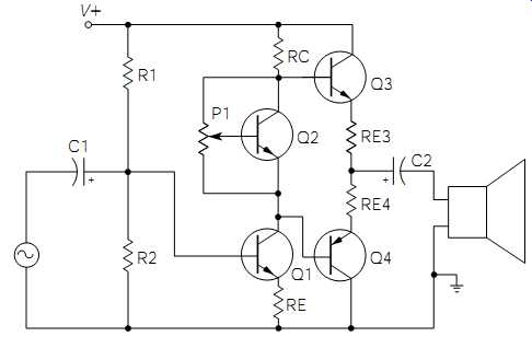
FIG. 2 A hypothetical class AB audio amplifier.
FIG. 2 is an example of a hypothetical class-AB audio amplifier. C1 is the input coupling capacitor, R1 and R2 form the familiar voltage divider bias network for biasing Q1, RE is Q1's emitter resistor, and RC is Q1's collector resistor. These components make up a typical common emitter transistor amplifier. Q2 and potentiometer P1 are configured in a circuit arrangement called an amplified diode. The purpose of this circuit is to provide the slight forward bias required on both output driver transistors to eliminate crossover distortion. Q3 and Q4 are the output drivers; with Q3 amplifying the positive half-cycles of the audio signal, and Q4 amplifying the negative half-cycles. C2 is an output-coupling capacitor; it serves to block the DC quiescent voltage from reaching the speaker, while allowing the amplified AC output voltage to pass.
The amplified diode circuit of Q2 and P1 could be replaced with two forward-biased diodes. In theory, each diode would drop about the same voltage as the forward biased base-emitter junction of each output transistor. The problem with this method is a lack of adjustment. If the for ward threshold voltage of each diode is not exactly equal to the base-emitter junction voltage of each transistor, some crossover distortion can occur. If three diodes are used, the quiescent conduction current of each output transistor might be too high, resulting in excessive heating of the output transistors.
The amplified diode circuit could also be replaced with an adjustable biasing resistor for biasing purposes. Although this system will function well and eliminate crossover distortion, the adjustable resistor will not thermally "track" with the output transistors. As you might recall, bipolar transistors have a negative temperature coefficient, meaning that they exhibit a decrease in resistance with an increase in temperature. In reference to transistors, a decrease in resistance actually means an increase in leakage current. In other words, bipolar transistors become more "leaky" when they get hot. In bipolar transistor amplifiers, this is a major problem. As output transistors begin to heat up, the leakage current also increases, causing an increase in heat, causing an increase in leakage current, causing an additional increase in heat, causing an additional increase in leakage current, and so forth. This condition will continue to degrade until the output transistors break down. A breakdown of this nature is called thermal runaway.
A means of automatic thermal compensation is needed to correct the problem. An adjustable resistor cannot do this (most resistors have a positive temperature coefficient), but that is the beauty of an amplifier diode circuit. Referring to FIG. 2, if Q2 is placed on the same heatsink as the output transistors, its temperature rise will closely approximate that of the output drivers. As the leakage current increases with a temperature rise in the output transistors, the leakage current through Q2 also increases. The increase of leakage current through Q2 causes the voltage drop across it to decrease, resulting in a decrease of forward bias to the output transistors. The decrease in forward bias compensates for the increase in leakage current, thus resulting in good temperature stabilization.
Additional Amplifier Classification
There are additional classes of amplifier operation, but they are not typically used for audio amplifiers. Class C amplifiers are biased to amplify only a small portion of a half-cycle. They are used primarily in RF (radio-frequency) applications, and their efficiency factors are usually about 80%.
Class D amplifiers are designed to amplify "pulses," or square waves. A class D amplifier is strictly a "switching device," amplifying no part of an input signal in a linear fashion. Strangely enough, class D amplifiers are available (although rarely) as audio amplifiers through a technique called pulse-width modulation (PWM). A PWM audio amplifier outputs a high-frequency (about 100 to 200 kHz) square wave to the audio speaker.
Because this is well above human hearing, the speaker cannot respond. But the duty cycle (on-time/off-time ratio) of the square-wave output is varied according to the audio input signal. In effect, this creates a proportional "power signal," which the speaker does respond to, and the audio input signal is amplified. Class D audio amplifiers boast extremely high efficiencies, but they are expensive, and they have drawbacks in other areas. Class D audio amplifiers are sometimes called digital audio amplifiers. Most class D amplifiers are more commonly used for high-power switching and power conversion applications.
Audio Amplifier Output Configurations
The circuit illustrated in FIG. 2 has a complementary symmetry output stage. This term means that the output drivers are of opposite types (one is NPN, and the other is PNP) but have symmetric characteristics (same beta value, base-emitter forward voltage drop, voltage ratings, etc.). Generally speaking, most audiophiles consider this to be the best type of output driver design. Transistor manufacturers offer a large variety of matched pair, or complementary pair, transistor sets designed for this purpose.
Another common type of output design is called the quasi-complementary symmetry configuration. It requires a complementary symmetry "predriver" set, but the actual output transistors are of the same type (either both NPN, or both PNP; NPN outputs are vastly more popular).
This type of output design used to be a lot more popular than it is now.
The current availability of a large variety of high-power, high-quality complementary transistor pairs has overshadowed this older design. However, it produces good-quality sound with only slightly higher-distortion characteristics than complementary symmetry.
Audio Amplifier Definitions
The field of audio electronics is an entertainment-oriented field. The close association between audio systems and the arts has led to a kind of semi-artistic aura surrounding the electronic and electromechanical systems themselves. As with any artform, personal preference and taste play a major role. This is the reason why there are so many disputes among audiophiles regarding amplifier and speaker design. My advice is to simply accept what sounds good to you, without falling prey to current trends and fads.
Unfortunately, there have been many scams and sly stigmas perpetrated by unethical, get-rich-quick manufacturers over the years. This has led to much misunderstanding and confusion regarding the various terms used to define audio amplifier performance.
The most heavily abused characteristic of amplifier performance is "power." Power, of course, is measured in watts. The only standardized method of designating AC wattage, for comparison purposes, is by using the rms value. Any other method of rating an amplifier's power output should be subject to suspicion.
Output power is also rated according to the speaker load. For example, an amplifier specification might rate the output power as being 120 watts rms into a 4-ohm load, and 80 watts rms into an 8-ohm load. You might expect the power output to double when going from an 8-ohm load to a 4-ohm load, but there are certain physical reasons why this will not happen. However, when comparing amplifiers, be sure to compare "apples with apples"; an amplifier rated at 100 watts rms into an 8-ohm load is more powerful than an amplifier rated at 120 watts rms into a 4-ohm load.
The human ear does not respond in a linear fashion to differing amplitudes of sound. It is very fortunate for you that you are made this way, because the nonlinear ear response allows you to hear a full range of sounds; from the soft rustling of leaves to a jackhammer pounding on the pavement. For example, a loud sound that is right on the thresh old of causing pain to a normal ear is about 1,000,000,000,000 times louder than the softest sound that can be heard. Our ears tend to "compress" louder sounds, and amplify smaller ones. In this way, we are able to hear the extremely broad spectrum of audible sound levels.
When one tries to express differing sound levels, power ratios, noise content, and various other audio parameters, the nonlinear characteristic of human hearing presents a problem. It was necessary to develop a term to relate linear mathematical ratios with nonlinear hearing response. That term is the decibel. The prefix deci means 1/10, so the term decibel actually means "one-tenth of a bel." The bel is based on a logarithmic scale. Although I can't thoroughly explain the concepts of logarithms within this context, I can give a basic feel for how they op e r at e . Logarithms are trigonometric functions, and are based on the number of decimal "columns" contained within a number, rather than the decimal values themselves. Another way of putting this is to say that a logarithmic scale is linearized according to powers of ten. For example, the log of 10 is 1; the log of 100 is 2; the log of 1000 is 3. Notice, in each case, that the log of a number is actually the number of weighted columns within the number minus the "units" column. The bel is a ratio of a "reference" value, to an "expressed" value, stated logarithmically. A decibel is simply the bel value multiplied by 10 (bels are a little too large to conveniently work with).
In this case, I believe a good example is worth a thousand words. Assume you have a small radio with a power output of 100 mW rms.
During a party, you connect the speaker output of this radio into a power amplifier which boosts the output to 100 watts rms. You would like to express, in decibels, the power increase. The power level that you started with, 100 mW (0.1 watt), is your reference value. Dividing this number into 100 watts gives you your ratio, which is 1000. The log of 1000 is 3 (bel value). Finally, multiply 3 by 10 (to convert bels to decibels), and the answer is 30 decibels.
Each 3-dB increase means a doubling of power: 6 dB gives 4 times the power [3 dB _ 3 dB equates to 2x power times 2x power; 2x(2x) _ 4x]. A 9-dB power increase converts to an 8x power increase [6 dB _ 3 dB, or 4x(2x) _ 8x].
Each 10-dB increase equals a 10-fold increase; for instance, 20 dB yields 100x [10 dB _ 10 dB, or 10x times 10x]. And finally, as per the example above, a 30-dB power gain means a 1000-fold increase [10 dB _ 10 dB _ 10 dB _ 10x3 _ 1000x].
Also, please be aware that negative values of decibels represent negative gain, or attenuation. A _3-dB gain means that the power has been halved. Similarly, a _10-dB gain represents a 10-fold attenuation, or a 0.1x change in power output.
These figures represent power logs. Voltage and current decibel logs are somewhat different: the square root of the power logs. This is because power is voltage times current, P _ IE; 30-dB volts is 31.620, and 30-dB amps is also 31.620. Thus, logP = logI x logE = 31.62 x 31.62=999.8x. Most electronic reference books have decibel log tables for easy reference. Just be aware that there is a difference between the power logs, and the voltage or current logs.
I recognize that if you have not been exposed to the concept of logarithms, or exponential numbering systems, this entire discussion of decibels is probably rather abstract. If you would like to research it further, most good electronics math books should be able to help you understand it in more detail.
Dynamic range is a term used to describe the difference (in decibels) between the softest and loudest passages in audio program material. In a practical sense, it means that if you are listening to an audio system at a 10-watt rms level, then for optimum performance, you would probably want about a 40-watt rms amplifier to handle the instantaneous high volume passages that might be contained within the program material (a cymbal crash, for example). Compact-disk and "hi-fi" (high-fidelity) videotape recorders offer the widest dynamic range commonly available in today's market.
Frequency response defines the frequency spectrum that an amplifier can reproduce. The normal range of human hearing is from 20 to 20,000 Hz (if you're a newborn baby, and had Superman as a father). In theory, there are situations occurring in music where ultrasonic frequencies are produced which are not audible, but without them, the audible frequencies are "colored" to some degree, causing a variance from the original sound. For this reason, many high-quality power amplifiers have frequency responses up to 100,000 hertz. The high-end and low-end frequency response limits are specified from the point where the amplifier power output drops to 50% (_3 dB) of its rated output.
Distortion is a specification defining how much an amplifier changes, or "colors," the original sound. A perfect amplifier would be perfectly "linear," meaning that the output would be "exactly" like the input, only amplified. However, all amplifiers distort the original signal by some percentage. In the mid-1970s, it was a commonly accepted fact that the human ear could not distinguish distortion levels below 1%. That has since been proved wrong. It is a commonly accepted rule of thumb today that even a trained ear has difficulty detecting distortion below 0.3%, although this figure is often disputed as being too high among many audiophiles. In any case, the lower the distortion specifications, the better.
Distortion is subdivided down into two more specific categories in modern audio amplifiers: harmonic distortion and intermodulation distortion. Harmonic distortion describes the nonlinear qualities of an amplifier. In contrast, intermodulation distortion defines how well an amplifier can amplify two specific frequencies simultaneously, while preventing the frequencies from interfering with each other in a nonlinear fashion.
Typical ratings for both of these distortion types is 0.1% or lower in modern high-quality audio amplifiers.
Load impedance defines the recommended speaker system impedance for use with the amplifier. For example, if the amplifier specification indicates the load impedance as 4 or 8 ohms, you might use either a 4- or 8-ohm speaker system (or any impedance in between) as the output load for the amplifier.
Input impedance describes the impedance "seen" by the audio input signal. This value should be moderately high: 10 Kohms or higher.
Sensitivity defines the rms voltage level of the input audio signal required to drive the amplifier to full output power. Typical values for this specification are 1 to 2 volts rms.
Signal-to-noise ratio is a specification given to compare the inherent noise level of the amplifier with the amplified output signal. Random noise is produced in semiconductor devices by the recombination process occurring in the junction areas, as well as other sources. High quality audio amplifiers incorporate various noise reduction techniques to reduce this undesirable effect, but a certain amount of noise will still exist and be amplified right along with the audio signal. Typical signal to-noise ratios are _70 to _92 dB, meaning that the noise level is 70 to 92 dB below the maximum amplifier output.
There are additional specifications that might or might not be given in conjunction with audio amplifiers, but the previous terms are the most common and the most important.
Before proceeding, here is a note of caution. Research has proved that continued exposure to high-volume noise (meaning music or any other audio program material) causes degradation of human hearing response. It saddens me to hear young people driving by in their cars with expensive audio systems blasting out internal sound pressure levels at 120 dB. Even relatively short exposures to this level of sound can cause them to develop serious nerve-deafness problems by the time they're middle-aged. Of course, exposure to high-volume levels at any age is destructive. It isn't worth it. Keep the volume down to reasonable levels for your ear's sake.
Power Amplifier Operational Basics
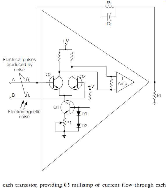
FIG. 3 Power amplifier operational basics.
Now that some of the basic audio terms have been established, this section will concentrate on the "front end" of modern audio amplifier design. In addition, this section establishes some of the basics relating to integrated circuit operational amplifiers, which will be discussed later in this guide.
FIG. 3 is a kind of semiblock diagram illustrating the input stage of most high-power audio amplifiers. Q1, D1, D2, and P1 form a circuit called a constant-current source. For discussion purposes, assume that D1 drops the same voltage as the base-emitter junction of Q1 (which should be a close assumption). That would mean that the voltage drop across D2 would also be the voltage drop across P1. If the voltage drop across D2/P1 is 0.7 volt, and P1 is adjusted to be 700 ohms, the emitter current flow will be 1 milliamp. Because the collector current of Q1 will approximately equal the emitter current, the collector current is also "held" at 1 milliamp. The important point to note here is that the collector current is regulated; it is not dependent on the collector load or the amplitude of the source voltage. The only variables controlling the collector current are D2's forward threshold voltage and the setting of P1. Therefore, it is appropriately named a constant-current source.
Transistors Q2 and Q3 form a differential amplifier. Think of a differential amplifier as being like a seesaw in a school playground. As long as everything is balanced on a seesaw, it stays in a horizontal position. If something unbalances it, it tilts, causing one end to go up proportionally, as the other end goes down. This is exactly how a differential amplifier operates with the current flow. As discussed previously, it is assumed that the constant current source will provide a regulated 1 milliamp of current flow to the emitters of Q2 and Q3. If Q2 and Q3 are in a balanced condition, the 1 milliamp of current will divide evenly between each transistor, providing 0.5 milliamp of current flow through each collector. If an input voltage is applied between the two base inputs (A and B) so that point A is at a different potential than point B, the balance will be upset. But as the collector current rises through one transistor, it must decrease by the same amount through the other, because the constant-current source will not allow a varying "total" current. For example, if the differential voltage between the inputs caused the collector current through Q2 to rise to 0.6 milliamp, the collector current through Q3 will fall to 0.4 milliamp. The total current through both transistors still adds up to 1 milliamp.
Notice that the output of the differential amplifier is not taken off of one transistor in reference to ground; the output of a differential amplifier is the difference between the two collectors. Now let's discuss the advantages of such a circuit.
Assume that the source voltage (supplied externally) increases. In a common-transistor amplifier, an increase in the source voltage will cause a corresponding change throughout the entire transistor circuit.
In FIG. 3, an increase in the source voltage (+V) does not cause an increase in current flow from the constant current source, because it is regulated by the forward voltage drop across D2, which doesn't change (by practical amounts) with an increase in current. Q2 and Q3 would still have a combined total current flow of 1 milliamp. The collector voltages of Q2 and Q3 would increase, but they would increase by the same amount, even if the circuit were in an unbalanced state.
Therefore, the voltage differential between the two collectors would not change. For example, assume that Q2's collector voltage is 6 volts and Q3's collector voltage is 4 volts. If you used a voltmeter to measure the difference in voltage between the two collectors, it would measure 2 volts (6 _ 4 _ 2). Now assume the source voltage increased by an amount sufficient to cause the collector voltages of Q2 and Q3 to increase by 1 volt. Q2's collector voltage would rise to 7 volts, and Q3's would rise to 5 volts. This didn't change the voltage differential between the two collectors at all; it still remained at 2 volts. In other words, the output of a differential amplifier is immune to power supply fluctuations. Not only does this apply to gradual changes in DC levels; the effect works just as well with power supply ripple and other sources of undesirable noise signals that might enter through the power supply.
One of the most common problems with high-gain amplifiers is noise and interference signals being applied to the input through the input wires. Input wires and cables can pick up a variety of unwanted signals, just as an antenna is receptive to radio waves. If you have ever touched an uninsulated input to an amplifier, you un-doubtably heard a loud 60-hertz roar (called "hum") through the speaker. This is because your body picks up electromagnetically radiated 60-hertz signals from power lines all around you. Fluorescent lights are especially bad electro magnetic radiators. FIG. 3 illustrates an example of some electromagnetic radiation causing noise pulses on the A and B inputs to the differential amplifier. Because electromagnetic radiation travels at the speed of light (186,000 miles per second), the noise pulses will occur at the same time, and in the same polarity. This is called common-mode interference. A very desirable attribute of differential amplifiers is that they exhibit common-mode rejection. The noise pulses illustrated in FIG. 3 would not be amplified.
To understand the principle behind common-mode rejection, assume that the positive-going noise pulse on the A input is of sufficient amplitude to try to cause a 1-volt decrease in Q2's collector voltage. Because the noise is common mode (as is all externally generated noise), an identical noise pulse on the B input is trying to cause Q3's collector voltage to decrease by 1 volt also. If both collectors decreased in voltage at the same time, it would require an increase in the combined total current flow through both transistors. This can't happen because the constant current source is maintaining that value at 1 milliamp.
Therefore, neither transistor can react to the noise pulse, and it is totally rejected. (Even if both transistors did react slightly, they would react by the same amount. Because the output of the pair is the difference across their collectors, a slight reaction by both at the same time would not affect their differential output.) This goes back to the analogy of the seesaw I made earlier. If a seesaw is balanced and you placed equal weights on both ends at the same time, it would simply remain stationary. In contrast, the desired signal voltage to be amplified is not common mode. For example, the B input might be at signal ground while the A input is at 1 volt rms. Differential amplifiers respond very well to differential signals. That is why they are called differential amplifiers.
One final consideration of FIG. 3 is in reference to RF and CF.
Notice that this resistor/capacitor combination is connected from the output back to one of the inputs. The process of applying a percentage of the output back into the input is called feedback. In high-gain amplifiers, this feedback is almost always in the form of negative feedback, meaning the feedback acts to reduce the overall gain. Negative feedback is necessary to temperature stabilize the amplifier, flatten out the gain, increase the frequency response, and eliminate oscillations. Various combinations of resistors and capacitors are chosen to tailor the frequency response, and to provide the best overall performance. Feed back will be discussed further in later sections.
Building High-Quality Audio Systems
You don't have to be an electrical engineer to build much of your own high-quality audio equipment. Even if your interests don't lie in the audio field, you are almost certain to need a lab-quality audio amplifier for many related fields. In this section, I have provided a selection of audio circuits that are time-proven, and which provide excellent performance.
FIG. 4 is a block diagram of a typical audio amplification system.
It is mostly self-explanatory, with the exception of the volume control and the two 10-uF capacitors. The volume control potentiometer should have an audio taper (logarithmic response). A typical value is 100 Kohms.
For stereo applications, this is usually a "two-ganged" pot, with one pot controlling the right channel and one pot controlling the left. The two 10-uF capacitors are used to block unwanted DC shifts that might occur if the volume control is rotated too fast.
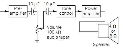
FIG. 4 Block diagram of a typical audio amplification system.
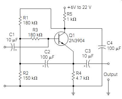
FIG. 5 Preamplifier for use with high-Z signal sources.
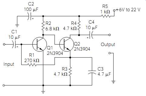
FIG. 6 High-gain preamplifier.
FIG. 5 is a simple preamplifier circuit for use with high-impedance signal sources, such as crystal or ceramic microphones. It is merely a common-collector amplifier with a few refinements. R5 and C4 are used to "decouple" the circuit's power source. The simple RC filter formed by R5 and C4 serves to isolate this circuit from any effects of other circuits sharing the same power supply source. R3 and C2 provide some positive feed back (in phase with the input) called "bootstrapping." Bootstrapping has the effect of raising the input impedance of this circuit to several Mohms.
FIG. 6 is a high-gain preamplifier circuit for use with very low input signal sources. Dynamic microphones, and some types of musical instruments (such as electric guitars), work well with this type of circuit.
R1 provides negative feedback for stabilization and temperature compensation purposes. Notice that this circuit is also decoupled by R5 and C2.
FIG. 7 is an active tone control circuit for use with the outputs of the previous preamplifier circuits, or any line-level output. Active tone controls incorporate the use of an active device (transistor, FET, operational amplifier, etc.), and can provide better overall response with gain. Passive tone controls, in contrast, do not use any active devices within their circuits, and will always attenuate (reduce) the input signal. Line-level outputs are signal voltages that have already been pre-amplified. The audio outputs from CD players, VCRs, tape players, and other types of consumer electronic equipment are usually line-level outputs.
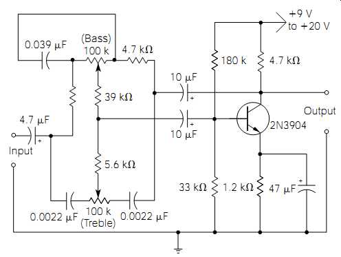
FIG. 7 Active tone control circuit.
FIG. 8 is a 12-watt rms audio power amplifier (the term power amplifier implies that the primary function of the amplifier is to provide low-impedance, high-current driving power to a typical loudspeaker system). It is relatively easy to construct, provides good linearity performance, and operates from a single DC supply (most audio power amplifiers require a dual-polarity power supply). A simple "raw" DC power supply, similar to the one illustrated in Fig. 4, constructed from a 2 amp, 24-volt transformer, a 2-amp bridge rectifier, and a 1000 uF filter capacitor at 50 working volts DC (WVDC) should power this circuit nicely (the rectified and filtered DC voltage produced from a 24-volt trans former will come out to about 36 volts DC). The complete circuit can be assembled on a small universal perfboard, or it can be constructed on its own PC board (PC circuit board fabrication is described later in this section; this project is mentioned here because it is ideal to test your first attempts at PC board making.) The parts list for this amplifier is given in Table 1.
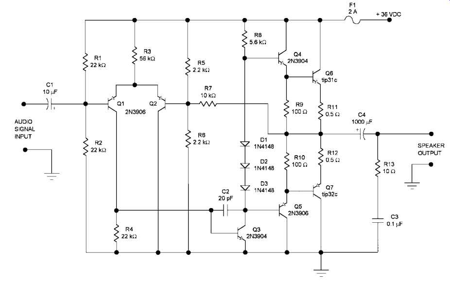
Fig. 8--A 12-watt rms audio power amplifier.
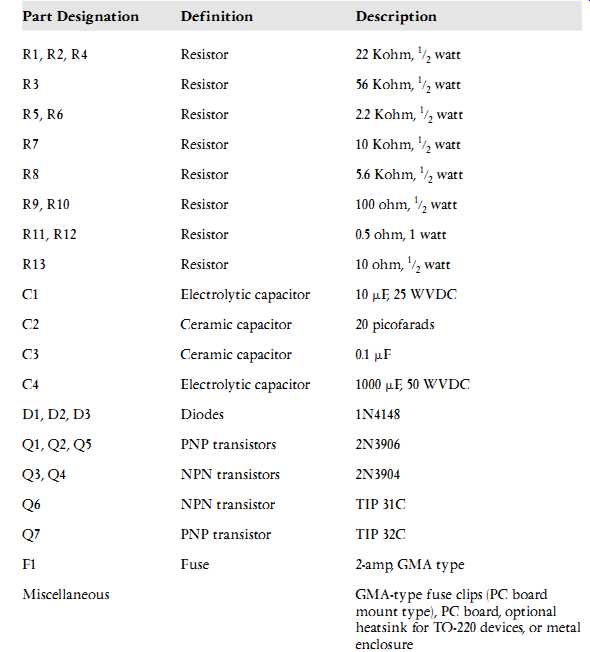
TABLE 1 Parts List for 12-Watt Audio Amplifier Project
A functional description of FIG. 8 is as follows. Beginning at the left hand side of the illustration, the "audio signal input" is a line-level signal from a preceding audio device, such as an FM receiver or cassette tape deck. C1 is a coupling capacitor, blocking the DC bias on the base of Q1 from being applied to the preceding audio device.
Transistors Q1 and Q2 make up a differential amplifier, which functions as the first amplification stage of the amplifier. Differential amplifiers are often chosen as the first stage of an audio amplifier because they provide a convenient point of applying negative feedback (i.e., the inverting input; the base of Q2), and because they are capable of high current gain and high input impedance and are relatively insensitive to power supply fluctuations. A differential amplifier's unique quality of common-mode rejection is a paramount issue pertaining to their use in operational amplifiers (discussed in Section 12), but it is not used at all within the context of most audio power amplifiers. A single resistor, R3, is used in place of a constant-current source, which is typically adequate for many medium-quality audio power amplifiers. R4 is the load resistor for the differential amplifier. Note that Q2 doesn't have a load resistor; this is because an output signal is not needed from Q2.
Resistors R1 and R2 form a voltage divider that splits the power sup ply in half, biasing the base of Q1 at half of the power supply voltage, or approximately 18 volts. Resistors R5 and R6 provide the identical function for the base of Q2. The combined voltage-dividing effect of R1, R2, R5, and R6 is to cause the entire amplifier circuit to operate from a reference of half of the power supply voltage, thereby providing the maximum peak-to-peak voltage output signal.
The second amplification stage of FIG. 8 is made up of Q3 and its associated components. This is a simple common-emitter amplifier stage, in which the audio signal is applied to the base of Q3 and the amplified output is taken from its collector. R8 serves as the collector load for Q3.
Diodes D1, D2, and D3 provide a small forward bias to Q4, Q5, Q6, and Q7, to reduce the effects of crossover distortion. Capacitor C2 functions as a compensation capacitor. Compensation is a common term used with linear circuits (especially operational amplifiers) referring to a reduction of gain as the signal frequency increases. High-gain linear circuitry will always incorporate some amount of negative feedback (as discussed previously, to improve the overall performance). At higher frequencies, because of the internal capacitive characteristics of semiconductors and other devices, the negative-feedback signal will increasingly lag the input signal (remember, voltage lags the current in capacitive circuits). At very high frequencies, this voltage lag will increase by more than 180 degrees, causing the negative-feedback signal to be "in phase" with the input signal. If the voltage gain of the amplifier is greater than unity at this frequency, it will oscillate. Therefore, compensation is the general technique of forcing the voltage gain of a linear circuit to drop below unity before the phase shifted negative feedback signal can lag by more than 180 degrees. In gist, compensation ensures stability in a high-gain amplifier or linear circuit.
To understand how C2 provides compensation in the circuit of FIG. 8, note that it connects from the collector of Q3 to the base of Q3. As you recall, the output (collector signal) of a common-emitter amplifier is 180 degrees out of phase with the input (base signal). Therefore, as the signal frequency increases, causing the impedance of C2 to drop, it begins to apply the collector signal of Q3 to the base of Q3. The 180-degree out-of phase collector signal is negative feedback to the base signal, so as the frequency increases, the voltage gain of Q3 decreases. The result is a falling-off (generally called rolloff) of gain at higher frequencies, promoting good audio frequency stability of the FIG. 8 amplifier.
All of the voltage gain in the FIG. 8 amplifier occurs in the first two stages. Therefore, when an audio signal is applied to the input of the amplifier, the signal voltage at the collector of Q3 will be the "maximum" output signal voltage that the amplifier is capable of producing.
There are two other points regarding the signal voltage at the collector of Q3 that should be understood. First, it is in phase with the input signal. This is because the original audio signal was inverted once at the collector of Q1, and it is inverted again at the collector of Q3, placing it back in phase with the input. Second, the audio input signal was super imposed on the DC quiescent level at the base of Q1, which is set to half of the power supply voltage, or about 18 volts. Therefore, a positive half cycle of the audio signal on the collector of Q3 will vary from 18 to 36 volts. In contrast, a negative half-cycle of the audio signal will vary from 18 volts down to 0 volt (i.e., the amplified AC signal voltage is superimposed on a quiescent DC level of half of the power supply voltage).
The third stage of FIG. 8 consists of Q4, Q5, Q6, Q7, and their associated components. To begin, consider the operation of Q4 and Q6 only. Note that they are both NPN transistors, and the emitter of Q4 connects directly to the base of Q6. This configuration is simply a type of Darlington pair with a few "stabilizing" resistors added. As you recall, the purpose of a Darlington pair is to increase the current gain parameter, or beta, of a transistor circuit. Transistors Q4 and Q6 serve as a high-gain, current amplifier in this circuit. They will current-amplify the collector signal of Q3.
Under normal operation, the quiescent DC bias of this amplifier is such that the right-hand side of R7 will be at half of the power supply voltage, or about 18 volts (this condition is due to the DC bias placed on the input stage, as explained earlier). This also means that the emitters of Q4 and Q6 will be at about 18 volts also (minus a small drop across their associated emitter resistors). If a positive-going AC signal is applied to the input of this amplifier, transistors Q4 and Q6 will current-amplify this signal. However, as soon as the AC signal goes into the negative region, the signal applied to the base of Q4 will drop below 18 volts, causing Q4 and Q6 to go into cutoff. Therefore, Q4 and Q6 are only amplifying about half of the audio signal (i.e., the positive half-cycles of the audio AC signal). Since transistors Q5 and Q7 are PNP devices, with their associated collectors tied to circuit common, they are current amplifying the negative half-cycles of the audio AC signal, in a directly inverse fashion as Q4 and Q6. Simply stated, all audio signal voltages above 18 volts are amplified by Q4 and Q6, while all audio signal voltages below 18 volts are amplified by Q5 and Q7. Consequently, the entire amplified audio signal is summed at the positive plate of C4.
Note that resistor R7 is connected from the amplifier's output back to the "inverting" side of the input differential amplifier (i.e., the base of Q2). R7 is a negative-feedback resistor. As you recall, the audio signal voltage at the collector of Q3 is in phase with the audio input signal. Q4, Q5, Q6, and Q7 are all connected as common-collector amplifiers (i.e., the input is applied to the bases with the output taken from the emitters). Since common-collector amplifiers are noninverting, the audio signal at the amplifier's output remains in phase with the input signal.
Therefore, the noninverted output signal that R7 applies back to the inverting input of the differential amplifier is negative feedback. Negative feedback in this circuit establishes the voltage gain, increases linearity (i.e., decreases distortion), and helps stabilize the quiescent voltage levels. The voltage gain (Ae ) of this amplifier is approximately equal to R7 divided by the parallel resistance of R5 and R6 (i.e., about 10).
Capacitor C4, like C1, is a coupling capacitor, serving to block the quiescent 18-volt DC level from being applied to the speaker. Note, however, that the value of C4 is very large compared to the value of C1. This is necessary because the impedance of most speakers is only about 8 ohms. Therefore, in order to provide a time constant long enough to pass low frequency audio signals, the capacity of C4 must be much greater.
Finally, resistor R13 and capacitor C3 form an output circuit that is commonly referred to as a Zobel network. The purpose of a Zobel net work is to "counteract" the effect of typical speaker coil inductances, which could have a destabilizing effect on the amplifier circuitry.
As you may have noted, the FIG. 8 amplifier consists of three basic stages, commonly referred to as the input stage (Q1 and Q2), the voltage amplifier stage (Q3), and the output stage (Q4, Q4, Q6, and Q7). Virtually all modern solid-state audio power amplifiers are designed with this same basic three-stage architecture, commonly referred to as the Lin three-stage topology.
Constructing the 12-Watt RMS Amplifier of FIG. 8
If you decide to construct this amplifier circuit on a universal bread board or solderless breadboard, the construction is rather simple and straightforward. You will need to provide some heatsinking for output transistors Q6 and Q7. If you mount the amplifier in a small metal enclosure, adequate heatsinking can be obtained by simply mounting Q6 and Q7 to the enclosure (remember to ensure that Q6 and Q7 are electrically isolated from the enclosure).
For optimum performance, diodes D1 and D3 should thermally track the temperature of transistors Q6 and Q7. This can be accomplished in several ways. The diodes could be glued to the case of the output devices with a small drop of epoxy, or you can bend a small solderless "ring" terminal into a makeshift clamp, with the ring held in place by the transistor's mounting bolt. If you construct the amplifier circuit similar to the FIG. 9a layout, you can simply bend the diodes into a touching position with the output transistors (remember to solder the diodes high above the board surface if you want to use this technique).
If you plan to use a current-limited power supply to test this amplifier circuit (such as the "lab-quality power supply" detailed in Sections 3 through 6), fuse F1 isn't necessary. If you provide operational power to this amplifier circuit with a simple raw DC power supply as mentioned earlier, F1 must be included for safety purposes. Also, keep in mind that if you accidentally "short" (short-circuit) the speaker output leads together, you will probably destroy one or both of the output transistors (i.e., Q6 and Q7).
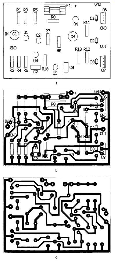
FIG. 9 12-watt audio amplifier: (a) and (b) top views silkscreen lay out;
(c) bottom view copper artwork.

FIG. 10 Illustration of a typical PC board fabrication kit.
Making Printed Circuit Boards by Hand
Making PC boards is not as difficult as you may have been led to believe, or as your past experiences may have indicated. Circuit board manufacture is a learned technique, and like any technique, there are several "correct" ways of going about it and many "wrong" ways of accomplishing disaster. In this section, I'm going to detail several methods that can be successfully used by the hobbyist. With a little practice, either of these methods should provide excellent results. The 12-watt audio amplifier described in the previous section is an excellent "first" project for getting acquainted with PC board fabrication, so I included a set of PC board layout illustrations in FIG. 9. See Section C for the full-size set to be used in your project.
To begin, you will need to acquire some basic tools and materials. If you are a complete novice regarding PC board construction, I recommend that you start by purchasing a "PC board kit," such as the one illustrated in FIG. 10. Typically, such kits will contain a bottle of etchant (an acid solution used to dissolve any exposed copper areas on the PC board), a resist ink pen (a pen used to draw a protective ink coating over any cop per areas that you don't want dissolved by the etchant), several "blank" (i.e., unetched) pieces of PC board material, and some miscellaneous supplies that you may or may not need. In addition, you will need a few very small drill bits (no. 61 is a good size), an electric hand drill, some fine grained emery paper, a small pin punch, a tack hammer, and a glass tray.
If you want to make a PC board of the FIG. 9 artwork by hand, the following procedure can be used. Begin by observing the illustrations provided in FIG. 9. FIG. 9a is commonly called the silkscreen layout.
It illustrates a top view of the placement and orientation of the components after they are correctly mounted to the PC board. FIG. 9b is another top view of the silkscreen, illustrating how the bottom-side copper artwork will connect to the top-mounted components-the PC board is imagined to be transparent. FIG. 9c is a reflected view of the bottom-side copper artwork. In other words, this is exactly how the cop per artwork should look if you turn the board upside down and look at it from the bottom. The reflected view of the copper artwork, FIG. 9c, is what you will be concerned with in the next phase of your PC board construction.
Make a good copy of FIG. 9c on any copy machine. Cut a piece of PC board material to the same size as the illustration. Cut out the illustration from the copy and tape it securely on the "foil" side of the PC board material. Using a small pin punch and tack hammer, make a dimple in the PC board copper at each spot where a hole is to be drilled.
When finished, you should be able to remove the copy and find a dimple in the copper corresponding to every hole shown in the artwork diagram. Next, drill the component lead holes through the PC board at each dimple position. When finished, hold the PC board up to a light, with the diagram placed over the foil side, to make certain you haven't missed any holes and that all of the holes are drilled in the right positions. If everything looks good, lightly sand the entire surface of the copper foil with 600-grit emery paper to remove any burrs and surface corrosion.
Using the resist ink pen, draw a "pad" area around every hole. Make these pads very small for now; you can always go back and make selected ones larger, if needed. Using single lines, connect the pads as shown in the artwork diagram in the following manner. Being sure you have the board turned correctly to match the diagram, start at one end and connect the simplest points first. Using these first points as a reference, eventually proceed on to the more difficult connections. When finished, you'll have a diagram that looks like a "connect the dots" picture in a coloring book. Finally, go back and "color" in the wide foil areas (if applicable) and fill in the wider tracks. The process is actually easier than it appears at first glance. If you happen to make a major mistake, just remove all of the ink with ink solvent or a steel wool pad and start over again-nothing is lost but a little time. You'll be surprised at how accomplished you will become at this after only a few experiences.
When you're satisfied that the ink pattern on the PC board corresponds "electrically" with the reflected artwork of FIG. 9c, place it in a glass or plastic tray (not metal!), and pour about an inch of etchant solution over it. Be very careful with this etchant solution; it permanently stains everything it comes in contact with, including skin. Wear goggles to protect your eyes, and don't breathe the fumes. After about 15 to 20 minutes, check the board using a pair of tongs to lift it out of the etchant solution. Continue checking it every few minutes until all of the unwanted copper has been removed. When this is accomplished, wash the board under cold water, and remove the ink with solvent or steel wool. When finished, the PC board will be ready for component installation and testing.
If you construct any PC boards using the aforementioned procedure, you will discover that the copper artwork on the finished PC board is slightly "pitted" in areas where the resist ink did not adequately protect the copper from the etchant. If you want to improve the finished quality of your PC boards, use inexpensive fingernail polish instead of resist ink. Obtain a dried-out felt-tipped marking pen (one with an extra-fine point), repeatedly dip the pen in the fingernail polish (like an old quill ink pen), and use it to draw your pads and traces in the same way that you would use the resist ink pen as described above. After etching, the fingernail polish can be removed with ordinary fingernail polish remover, and the copper foil surface of your PC board will be totally free of any pits or corrosion from the etchant.