AMAZON multi-meters discounts AMAZON oscilloscope discounts
Making Printed Circuit Boards by the Photographic Method
The previously described method of fabricating PC boards by hand is acceptable for some surprisingly complex PC patterns, but it is very time-consuming and non-repeatable (i.e., it is difficult to make exact replications). The serious hobbyist will most certainly develop the need to make PC boards in a more rapid and repeatable manner, and the best system that I have discovered for accomplishing this is by means of a photographic process. As in the case of the method discussed above, the photographic method of PC board fabrication is a learned technique, requiring a minimal amount of trial-and-error learning experience for optimum results. Don't get discouraged if your first attempt turns out less than ideal.
In addition to the previously listed materials, the photographic method of making PC boards will require some additional tools and materials. The PC board "blanks" will need to be pre-sensitized with a positive-acting photoresist. Such pre-sensitized PC boards are available from a wide variety of electronics suppliers, and the price is very reasonable. You will need a fluorescent light source, consisting of two ordinary 18-inch fluorescent lights positioned side by side, that can be placed approximately 2 inches above the surface of the PC board material. You will also need a supply of office transparencies that can be used with typical copy machines, available from office supply stores.
And finally, you will need some positive PC board developer (available from electronics suppliers; can be purchased as a dry powder or liquid) and a pane of glass somewhat larger than any PC board size that you intend to make.
The process of making a PC board with the positive photographic method is as follows. Begin by making a photopositive of the "reflected" PC board artwork that you intend to fabricate. This is accomplished by making a copy of the black-and-white reflected artwork illustration onto a sheet of clear transparency with a copy machine. The finished photopositive should look identical to the reflected artwork illustration (i.e., all of the copper areas to be saved are black; the copper areas to be etched are transparent), except that the white areas on the original illustration will be transparent on the photopositive. This dark area on this photopositive must be as opaque as possible. If you can see "leakage light" through the dark areas when holding the photopositive up to a light source, you should adjust the copier for a darker copy. If the copy is still too light, you may need to make two copies, and tape one copy over the other for increased opacity.
Once the photopositive is finished, you are ready to expose and develop the PC board artwork. Adjust the ambient lighting of your work area so that it is as dark as possible, but light enough to allow you to see what you're doing. Remove the protective plastic film from the pre-sensitized PC board material, and lay the PC board down (sensitized side up) onto a flat work surface. Place the photopositive on top of the pre-sensitized surface of the PC board, and then place the pane of glass on top of the photopositive (i.e., the photopositive is sandwiched flat between the pre sensitized surface and the pane of glass). At this point, make sure that the placement of the photopositive is correct on the PC board surface and that you haven't accidentally turned the photopositive upside down (getting the photopositive upside down is a very easy mistake to make- I've done it many times!). If all looks good, adjust your fluorescent lights to about 2 inches above the surface of the pane of glass. Turn on the fluorescent lights and expose the PC board for about 8 minutes.
After the exposure time is completed, remove the glass pane and photopositive, and store them for future use. Place the exposed PC board in a plastic or glass tray containing the "positive PC board developer solution." The recommended quantities of developer solution and mixing instructions will vary with different manufacturers, so follow the directions for preparing the developer solution as indicated on the specific type that you purchase. When the exposed PC board is placed in the developer solution, the photoresist coating that has been exposed to the fluorescent light will begin to dissolve, leaving a clear pattern of the desired PC board artwork. When all of the exposed photoresist has dissolved away, leaving a clean and bright copper surface underneath, remove the PC board from the developer solution and rinse under cold running water.
After the developed PC board has dried, examine the photoresist pat tern carefully. If there are numerous "pits" or "light-colored areas" in the photoresist surface, this means you suffered some bleed-through of fluorescent light through your photopositive. In this case, you need to increase the opacity (i.e., darkness) of the foil pattern on your photopositive. If the pitting and/or lightness of the photoresist is not excessive, you can touch up the photoresist pattern with a little fingernail polish.
Otherwise, you should scrap the PC board, correct your photopositive, and try again. In contrast, if some of your exposed copper areas (i.e., the areas intended to be etched) have a little remaining photoresist on them, this means that you didn't leave the PC board in the developer solution long enough. The only remedy is to scrape the excess photoresist off of the copper areas intended to be etched, but if the PC board artwork is more than moderately complex, it will probably be more practical to scrap the PC board and try again.
Assuming that you examine the developed PC board and everything looks good (i.e., the copper areas to be etched are bright and clean, the photoresist areas are smooth and pit-free, and all of the artwork edges are neat and sharp), the PC board is now ready for etching. This is accomplished in the same manner as described previously for making PC boards by hand. After the etching is completed, the photoresist can be removed with a fine steel wool pad, fingernail polish remover, or a variety of solvents. Personally, I like to use a spray can of "flux remover" for removing the photoresist.
If this whole photographic fabrication process sounds a little formidable, it is probably due to the lengthy and detailed description of the process that must be contained in a textbook of this sort. You might be a little shaky during your first attempt, but after a few experiences you'll easily get the hang of it. My wife has observed me making PC boards on many occasions, and she considers the whole process much less complicated than her recipe for good chicken gravy!
Other Methods of Fabricating PC Boards
As your experience in the electrical and electronics fields continues to grow, you will doubtless encounter various other methods of fabricating PC boards. Depending on your talents and resources, you may want to try a few. Generally speaking, the following is what I have discovered regarding some other popular methods.
The various methods used by large manufacturers and professional PC board fabrication companies can certainly produce professional-quality PC boards. However, the equipment and techniques required are typically too expensive for the hobbyist.
Although the photographic method, as previously described, will take more time per unit, the end results can be just as good as the professional manufacturing techniques.
The various types of "stick-on transfers" are adequate for small, uncomplicated, one-of-a-kind PC boards. However, for PC boards of medium complexity, the "fabrication by hand technique," as first described in this section, is typically faster and provides better results (it's also less frustrating than trying to work with those little sticky lines that seem to want to stick to everything except your PC board!).
The negative-acting photographic method is equal to the positive-acting method as described above. However, the materials are not as readily available, and, in some cases, it is more difficult to obtain a good "photonegative" of the PC board artwork.
The iron-on image-transfer system has become popular. With this method, you must purchase a special film intended for this technique from one of several manufacturers. The PC board artwork is copied onto the film using a copy machine or laser printer (the toner causes a chemical change on the film, making the transfer possible). The PC board artwork image is then directly ironed onto the PC board using a clothing iron or some other suitable heat source and pressure. Some hobbyists appear to favor this method, but I have not found the quality of the results to be equal to those using the photographic method. Also, the results are not as repeatable.
CAD Methods of PC Board Development
Before leaving this discussion on PC board fabrication, I would like to briefly describe the newer generation of CAD (i.e., computer-automated design) programs available for PC board development. In bygone days, an electrical engineer was forced to sit down with a schematic diagram, a tablet of graph paper, and a sordid collection of templates, rulers, and other drawing instruments, in the attempt to design a PC board layout for a new circuit design. This was usually an aggravating and time-consuming project, requiring the engineer to draw out trial-and-error track runs, reposition component placement, and redefine board dimensions, and all the while the designer had to think in an upside-down perspective as to how the track runs on the bottom of the board would connect to the component leads on top. As PC board complexities increased, this process became proportionally more difficult-in the case of modern multilayer PC boards, it became virtually impossible.
During the 1970s and 1980s, industry began developing various CAD programs to facilitate the difficult task of PC board layout design. Later, these CAD programs were "humanized" to make them more "user friendly," and marketed to electronic hobbyists for the purpose of designing "home-brew" PC boards. Currently, these PC board layout pro grams are available at modest pricing, and they are so easy to use that almost anyone can design PC boards at home. If you anticipate that you will be involved with electronics as an ongoing hobby or profession, I highly recommend that you purchase a good PC board layout program. It will be well worth the investment.
If you are new to CAD PC board layout programs, you may be wondering how you would use such a tool in a practical way. Allow me to provide a hypothetical example. Suppose you wanted to construct a small, portable guitar amplifier with tone control. You could combine the preamplifier circuit of FIG. 6 with the tone control circuit of Fig. 7 and the 12-watt power amplifier of FIG. 8. Obviously, you could con struct all of these circuits using perfboard or a universal breadboard, but the process is time-consuming and the finished product doesn't look very professional. In contrast, it would probably take you about an hour and a half to combine all three of these circuits into a single circuit design, download to a layout program, and come up with a single, finished, professional-quality PC board design. You would then use your inkjet printer to print out a full-size reflected artwork diagram directly onto a transparency. It may take you another hour to expose, develop, and etch the PC board for your project using this transparency. If you continued to work consistently, it might take you another 2 hours to drill the holes into the PC board and construct the finished project (provided you had all of the components on hand). In other words, you took a moderately complex project from the "idea" stage to the "professional-quality, completed project" stage in less than 5 hours! Your materials cost for this project was the cost of the pre-sensitized PC board blank (possibly two or three dollars, depending on size), less than one dollar's worth of chemicals, the transparency used in your inkjet printer (about 60 cents), and the cost of the electronic components.
If you are intimidated by the thoughts of "designing with computers" or "running complex programs," you shouldn't be. Most of these types of user-friendly CAD programs are self-explanatory and very easy to become comfortable with. Personally, I use the Electronics Workbench brand Multisim and Ultiboard design programs, and I can testify that on the very first time I tried using these programs, I was designing circuits in less time than it took me to figure out what the opening icons meant in Windows 95. And don't get the idea that I'm some sort of genius computer hacker-I still haven't made it through Windows ' 95 for Dummies.
A Professional-Quality Audio Power Amplifier
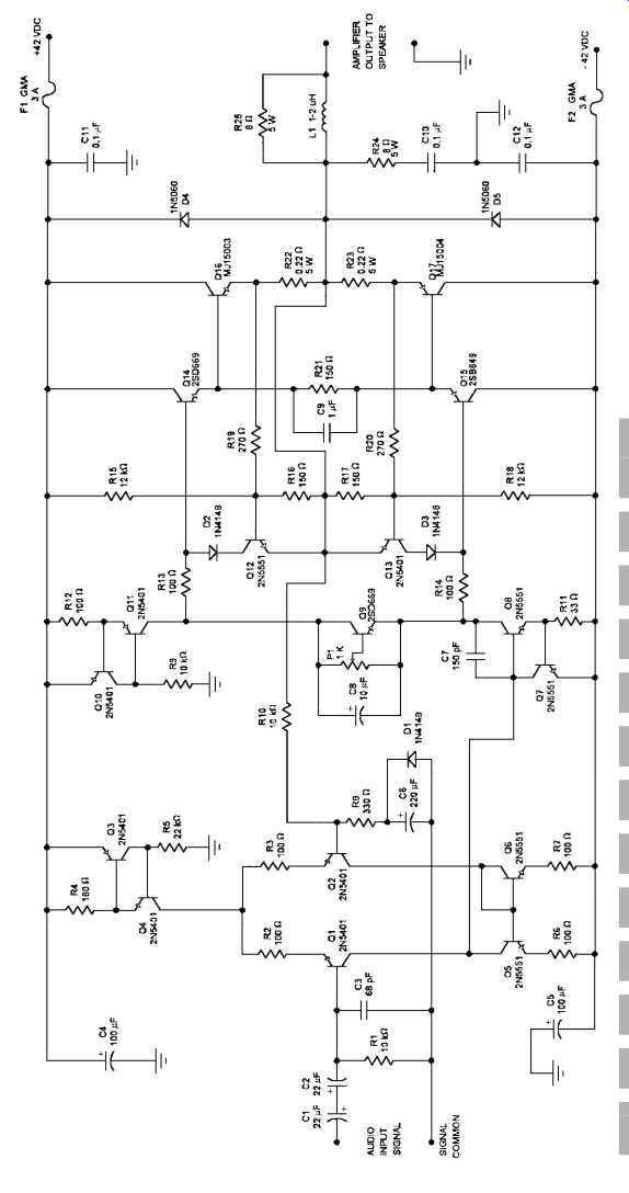
FIG. 11 Schematic diagram of a professional-quality audio power amplifier.
FIG. 11 is a schematic illustration of a very high-quality professional audio power amplifier. Modern high-quality, solid-state audio power amplifiers are a culmination of almost all of the commonly used linearization techniques applied to the entire field of linear electronic circuits. Therefore, a detailed dissection of the building blocks incorporated into a modern power amplifier is a very good method of understanding much of the theory and physics involved with the broad spectrum of linear electronics, including such subjects as operational amplifiers, servo systems, and analog signal processing. Also, it should be remembered that the humble audio amplifier is probably the most common electronic subsystem to be found in the vast field of consumer electronics, including such common devices as televisions, stereo systems, radios, musical instrument amplifiers, multimedia computer systems, and public address systems.
Preconstruction and Preliminary Design
The amplifier design of FIG. 11 is not a typical commercial-quality design; it is significantly superior. I chose this particular design to provide a baseline for discussion and illustration of various discrete building blocks that are commonly used in linear circuits. Also, it is a good project if you wish to construct something a little more advanced, and I have provided the PC board artwork if you would like to practice your PC board construction skills. (Unfortunately, space restrictions will not allow me the opportunity to provide PC board artwork for the majority of projects in this textbook-this is where a good CAD PC board design program will come in very handy!) Beginning with C1 and C2 in FIG. 11, note how they are connected in series, oriented with opposing polarities. This is a common method of creating a nonpolarized electrolytic capacitor from two typical electrolytic capacitors. The combination of C1 and C2 will look like a single nonpolarized capacitor with a capacitance value equal to half of either individual capacitor and a voltage rating equal to either one of the capacitors individually. In other words, if C1 and C2 are both rated at 22 uF at 35 WVDC, the equivalent nonpolarized capacitor will perform like an 11-uF capacitor at 35 WVDC. A nonpolarized coupling capacitor is needed for this amplifier because the quiescent voltage on the base of Q1 will be very close to circuit common potential, so the AC input signal current flow through C1 and C2 will be in both directions.
Degeneration (Negative Feedback)
R1 establishes the input impedance of the amplifier at approximately 10 kohms (the input impedance at the base of Q1 is much higher than R1). C3 provides some high-frequency filtering to protect the amplifier from ultrasonic signals that could be superimposed on the audio signal. R2 and R3 are degeneration resistors for the differential amplifier, consisting of Q1 and Q2. The term degeneration is used to describe a type of negative feedback and usually applies to resistors placed in the emitter circuits of transistors, but it can be applied to other techniques in which a single resistor is placed in the signal path of a gain stage, providing a voltage drop that opposes the gain action of an active device, thereby reducing gain and improving linearity. In simple terms, degeneration resistors flatten out the gain response of transistor circuits and improve their linearity.
Constant Current Sources
The circuit consisting of Q3, Q4, and R4 is an upside-down version of the circuit illustrated in Fig. 8d of the Transistor Workshop section of Section 6. If you refer back to Fig. 8d and the corresponding description, you will note that the Fig. 8d circuit serves the function of providing current-limit protection. In other words, it allows current to flow up to a maximum level, and then restricts it at that maximum level regardless of increases in the load or input signal. Referring back to FIG. 11, note that R5 has been added to the basic circuit of Fig. 8d, which provides a constant maximum base signal to Q4, which forces Q3 into a constant state of current limiting. Since the collector current of Q4 is constantly at the current-limit level (determined by the resistance value of R4), the circuit of Q3, Q4, R4, and R5 makes up a constant current source.
Actually, this type of constant-current source provides better performance than do the more conventional types of constant-current sources, such as illustrated in Fig. 6-8a. This is due to the fact that you have the combined effect of both transistors in regulating the current, instead of a single transistor referencing a voltage source. Note that the circuit consisting of Q10, Q11, R9, and R12 makes up an identical constant-current source for the voltage amplifier stage; however, the level of regulated current is set differently because of the resistance value of R12.
Current Mirrors Now, turn your attention to the peculiar-looking circuit consisting of Q5, Q6, R6, and R7 in FIG. 11. If you ever study the equivalent schematic diagrams of linear integrated circuits, you will see tons of these circuits represented. They are called current mirrors.
Current mirrors "divide" current flows into equal portions. For example, if 4 milliamps of current is flowing through the collector of Q4, the current mirror of Q5 and Q6 will force 2 milliamps to flow through Q1 and 2 milliamps to flow through Q2-it will divide the total current flowing through the differential amplifier equally through both legs.
This is important because a differential amplifier will be most linear when the current flows through both legs are "balanced" (i.e., equal to each other). Therefore, by incorporating the current mirror of Q5 and Q6, the linearity of the differential amplifier (i.e., Q1 and Q2) is optimized. The operational physics of Q5 and Q6 is rather simple. Since the collector of Q6 is connected directly to its base, the current flow through the collector of Q2 will be directly proportional to the voltage drop from the base to emitter of Q6. Since Q5's base-emitter junction is connected in parallel with Q6's base-emitter junction, Q5 is forced to "imitate" the collector current flow of Q6. Therefore, whatever the total current flow through the differential amplifier happens to be, it will be forced into a balanced state. R6 and R7 are degeneration resistors, serving to flatten out the small parameter differences between Q5 and Q6.
Voltage Amplification
Q8 provides the same function in this amplifier design as Q3 provides in the FIG. 8 amplifier. Namely, it provides the majority of "voltage gain" inherent to the amplifier. Likewise, C7 is the compensation capacitor for this amplifier, serving the same function as C2 does in the FIG. 8 amplifier.
Instead of utilizing three forward-biased diodes (to provide a small forward voltage drop, reducing the effects of crossover distortion) as in the design of FIG. 8, the amplified diode circuit of Q9, P1, and C8 is incorporated into the FIG. 11 design. Amplified diode circuits are often called Vbe multiplier circuits. An amplified diode circuit has the advantages of a more precise control of the continuous forward bias applied to the output transistors, as well as improved thermal tracking characteristics when the Vbias transistor (Q9 in this case) is physically mounted to the same heatsink as the output transistors. C8 provides smoothing of voltage variations that would normally appear across the amplified diode circuit during signal variations.
Active Loading
If you compare the amplifier design of FIG. 11 with the design of FIG. 8, you'll note that the collector load for the voltage amplifier transistor (R8 in FIG. 8) has been replaced with the Q10/Q11 constant-current source in FIG. 11. The technique of using a resistor (a passive device) for a collector load in a transistor amplifier is appropriately called passive loading. In contrast, the technique of using an active circuit for a collector load, such as the Q10/Q11 constant-current source, is called active loading.
The principles and reasons for active loading relate back to the basic operational fundamentals of a simple common emitter amplifier. As you may recall, the voltage gain of a common emitter amplifier is deter mined by the ratio of the emitter resistance to the collector resistance. In theory, if you wanted a common-emitter amplifier with a very high gain, you would be forced to make the collector resistor a very high resistance value. Unfortunately, as you may also recall, the output impedance of a common-emitter amplifier is approximated as the value of the collector resistor. Therefore, if you increase the resistance of the collector resistor to extremely high values, the amplifier's output impedance also increases to such high values that the amplifier is no longer capable of "matching" to any kind of practical load. In other words, it can't "drive" anything. The optimum collector load for a common-emitter amplifier would be a load that appeared to represent extremely high resistance (i.e., a high internal impedance), while simultaneously providing its own "drive current" to an external load. This is the effect that a constant-current source provides to a common emitter amplifier.
The easiest way to understand the desirable effects of active loading is to imagine Q8 in FIG. 11 to be a variable resistor (signal voltages applied to the base of Q8 will cause the collector-to-emitter impedance of Q8 to vary proportionally, so this imaginary perspective is not in error). Also, consider Q7 and the amplified diode circuitry to be out of the circuit for purposes of discussion. Imagine that the variable collector-to-emitter impedance provided by Q8 can range from the extremes of 100 ohms to 6 Kohms, which is a reasonable estimation. Assume that throughout this entire drastic range of collector-to-emitter impedance variations, the constant current source of Q10/Q11 maintains a constant, regulated current flow of 6.7 milliamps. The only way that the same "constant current" effect could be accomplished using "passive" loading would be to make the collector load resistance for Q8 extraordinarily high, so that Q8's collector-to-emitter impedance variations would be negligible. In other words, if the Q10/Q11 constant-current source were replaced with a 1-Mohm resistor (i.e., 1,000,000 ohms), the 100-ohm to 6-Kohm collector-to-emitter impedance variations of Q8 would have a negligible effect on the circuit current (i.e., the dominant current-controlling factor would be the very high resistance of the collector resistor). However, to accomplish a 6.7-milliamp current flow through a 1-Mohm resistor, you would need a 6700-volt power supply! Consequently, the "active load" provided by the constant current source of Q10/Q11 looks like a very high-resistance collector load to Q8, which improves the gain and linearity factors of this voltage amplifier stage.
Output Stage Considerations
Note that the collector circuit of Q8 must provide the signal drive current to the bases of Q14 and Q15 (through resistors R13 and R14). The technique of active loading, as previously described, also aids in providing some of the signal drive current to Q14 and Q15, which makes the output impedance of the Q8 voltage amplifier stage appear reasonably low. This desirable condition also improves the linearity of the voltage amplifier stage.
Transistors Q14, Q15, Q16, and Q17 in FIG. 11 perform the same function as described previously for transistors Q4, Q5, Q6, and Q7 in the 12-watt amplifier of FIG. 8. Collectively, these transistors constitute a "near-unity voltage gain, current amplifier." They are biased in a class B mode, meaning that Q14 and Q16 provide current gain for the positive half-cycles of the AC signal, while Q15 and Q17 provide current gain for the negative half-cycles of AC signal.
Capacitor C9 in FIG. 11 aids in eliminating a type of distortion known as switching distortion. High-power bipolar transistors have to be manufactured with a rather large internal crystal geometry to be able to handle the higher current flows. The larger crystal area increases the inherent "junction capacitance" of power transistors. The higher junction capacitance can cause power transistors to be reluctant to turn off rapidly (i.e., when they are driven into cutoff). If one output transistor is so slow in turning off that it is still in conduction when its complement transistor turns on, a very undesirable condition occurs which is referred to as cross conduction (i.e., both complementary output transistors are on at the same time). Cross-conduction creates switching distortion. Note how C9 is connected across both base terminals of the output transistors in FIG. 11.
Under dynamic operating conditions, C9 acts to neutralize charge carriers in the base circuits of the output transistors, thereby increasing their turn off speed and eliminating switching distortion. Although cross-conduction creates undesirable switching distortion in audio power amplifiers, it can be destructive in various types of motor control circuitry utilizing class B outputs. Consequently, it is common to see similar capacitors across the base circuits of high-current class B transistor outputs utilized in any type of high-power control circuitry.
Diodes D4 and D5 in FIG. 11 can be called by many common names. They are most commonly known as freewheeling, catching, kickback, or suppression diodes, although I have heard them called by other names.
Their function is to suppress reverse-polarity inductive "kickback" transients (i.e., reverse electromotive force pulses) that can occur when the output is driving an inductive load. As you may recall, this is the same function performed by D1 in Fig. 7-9 of Section 7.
Most high-quality audio power amplifiers will incorporate a low inductance-value air-core coil on the output, such as L1 in FIG. 11. L1 has the tendency to negate the effects load capacitance, which can exist in certain speakers or speaker crossover networks. Even small load capacitances can affect an audio power amplifier in detrimental ways, because it has a tendency to change the high-frequency phase relationships between the input and negative-feedback signals. Compensation is incorporated into an amplifier to ensure that its gain drops below unity before the feedback phase shift can exceed 180 degrees, resulting in oscillation. However, if the amplifier's speaker load is somewhat capacitive, it can cause a more extreme condition of phase lag at lower frequencies, leading to a loss of stability in the amplifier. At higher frequencies, the inductive reactance of L1 provides an opposing force to any capacitive reactance that may exist in the speaker load, thereby maintaining the stability of the amplifier under adverse loading conditions. The inductance value of L1 is too low to have any effect on frequencies in the audio bandwidth. R26, which is in parallel with L1, is called a "damping" resistor. R26 reduces "ringing oscillations" that can occur at resonant frequencies of the speaker and L1 (resonance will be discussed in a later section).
Short-Circuit Protection
The circuit consisting of Q12, D2, R16, R15, and R19 provides short-circuit protection during positive signal excursions for output transistor Q16. Likewise, Q13, D3, R17, R18, and R20 provide short-circuit protection for Q17 during negative signal excursions. Since these two circuits operate in an identical fashion but in opposite polarities, I will discuss only the positive protection circuit, and the same operational principles will apply to the negative circuitry.
Referring to FIG. 11, imagine that some sort of adverse condition arose, creating a direct "short" from the amplifier's output to circuit common.
Note that all of the speaker load current flowing through Q16's emitter must also flow through R22. As the Q16 emitter current tries to increase above 3 amps, the voltage drop across R22 (which is applied to the base of Q12 by R19) exceeds the typical 0.7-volt base-emitter voltage of Q12, causing Q12 to turn on. When Q12 turns on, it begins to divert the drive current away from the base of Q14, which, in turn, decreases the base drive current to Q16. The more the emitter current of Q16 tries to increase, the harder Q12 is turned on, thereby limiting the output current to a maximum of about 3 amps, even under a worst-case short-circuit condition. In other words, under an output short-circuit condition, this protection circuit behaves identically to the other current-limit protection circuits you have examined thus far. The only difference is the inclusion of Q14, which serves only to "beta-enhance" the output transistor Q16.
In addition to protecting the amplifier of FIG. 11 from short-circuit conditions at the output, the protection circuit also provides a more complex action than does simple current limiting. The voltage divider of R15 and R16, in conjunction with the dynamic action of the output rail (which is connected to the emitter of Q12), causes the current-limit action of the protection network to be "sloped." In other words, it will limit the maximum current to about 3 amps when the output rail voltage (i.e., the amplifier's output voltage) is 0 volt. However, as the output rail voltage increases in the positive direction, the protection circuitry will allow a higher maximum current flow. For example, if the amplifier's output voltage is at 20 volts, the protection circuit may allow a maximum of 5 amps of current flow. This type of sloped protection response allows the maximum output power to be delivered to a speaker system, while still providing complete protection for the output transistors. And finally, diode D2 is placed in the collector circuit of Q12 to keep Q12 from going into a state of conduction during negative signal excursions.
Now that the output protection circuitry has been explained, it becomes easier to understand the function of Q7. Q7 provides current limit protection for transistor Q8. If you refer back to Fig. 8d, (section 6) you will note that the Q7/Q8 combination of FIG. 11 is nearly identical; the only difference is in the value of the emitter resistors. To understand why Q8 in FIG. 11 needs to be current-limited, imagine that the amplifier output is short-circuited. If a positive signal excursion occurs, Q16 will be protected by Q12 turning on and essentially shorting (short-circuiting) Q14's base current to the output rail. In this situation, the drive current to Q14's base is actually originating in the constant-current source of Q10/Q11. Since Q10 and Q11 are already in a state of current limit, Q12's shorting action is of no consequence. However, if a negative signal excursion occurs, Q13 will turn on to protect Q17, shorting Q15's drive current to the output rail. During negative signal excursions, the drive current for Q15 is the collector current of Q8 through the negative power supply rail. Without the current-limit protection provided by Q7, Q8 would be destroyed as soon as Q13 turned on, because there would be nothing in the collector circuit of Q8 to limit the maximum current flow.
Negative Feedback Negative feedback in the FIG. 11 amplifier is provided by R8, R10, and C6. As you recall from previous studies of the common emitter amplifier, a "bypass" capacitor could be placed across the emitter resistor, causing the DC gain response to be different than the AC gain response. C6 serves the same purpose in this design of Fig. 11. The AC voltage gain response of this design is determined by the ratio of R10 and R8, since C6 will look like a short to circuit common to AC signal voltages. With the values shown, it will be about 31 [ (R10 _ R8) divided by R8 _ 31.3]. In contrast, C6 will look like an infinite impedance to DC voltages, placing the DC voltage gain at unity (i.e., 100% negative feedback). Simply stated, the negative-feedback arrangement of FIG. 11 provides the maximum negative DC feedback to maintain the maximum accuracy and stability of all DC quiescent voltages and currents. Regarding AC signal voltages, it provides the necessary voltage gain to provide the maximum output power to the speaker load.
Note that C6 is in parallel with D1. If a component failure happened to occur that caused a high negative DC voltage to appear on the output of the amplifier, a relatively high reverse-polarity voltage could be applied across C6, resulting in its destruction. Diode D1 will short any significantly high negative DC levels appearing across C6, thereby protecting it.
Other Concerns
Finally, a few loose ends regarding FIG. 11 have not been discussed. R24 and C10 make up the Zobel network, which serves the same purpose as the Zobel network previously explained in reference to FIG. 8. C11, C12, C4, and C5 are all decoupling capacitors for the power supply rails. You'll note that the "signal common" connection at the input of the amplifier is not connected to circuit common. This signal common point must be connected to circuit common, but it is better to run its own "dedicated" circuit common wire back to the power supply, thereby eliminating electrical noise that might exist on the "main" circuit common wire connecting to all of the other components.
Now that you have completed the theoretical analysis of the complex audio power amplifier of FIG. 11, as well as the other circuits illustrated in this section, you may be wondering how an in-depth understanding of these circuits will be beneficial in your continued involvement in electronics. Allow me to explain. If you happen to be interested in audio electronics, obviously this section is right down your alley. But if your interest lies with robotics or industrial control systems, don't despair! If you look at a schematic diagram of a servo motor controller, you'll say, "Hey! This is nothing but a customized audio power amplifier." If you look at the schematic of an analog proportional loop controller, as used extensively in industry, you'll say, "Hey! This is nothing but an adjustable gain amplifier with the means of obtaining negative feedback from an external source." If you look an the "internal" schematic of an operation amplifier IC, you'll say, "Hey! This is exactly like an audio power amplifier with external pins for customizing the feedback and compensation." (In reality, modern audio power amplifiers are nothing more than large "discrete" versions of operational amplifiers-you'll examine operational amplifiers in more detail in Section 12.) Expectedly, there will be times when you look at the schematic of an electronic circuit and say, "Hey! I have no idea what this is." However, if the circuit is functioning with analog voltages, currents, and/or signals, it will consist of some, or all, of the following circuit building blocks: single-stage or multistage amplifiers, differential amplifiers, current mirrors, constant-current sources, voltage reference sources, protection circuits, power supplies, and power supply regulation and protection circuits. It will also probably utilize some or all of the following techniques: beta enhancement, negative feedback, active loading, compensation, filtering, decoupling, and variations of gain manipulation. The only exception to these generalities will be in circumstances where the electronic circuitry consists primarily of linear integrated circuits performing the aforementioned functions and techniques. The main point is that if you have a pretty good understanding of the linear circuitry discussed thus far, you have a good foundation for comprehending the functions and purpose of most linear circuitry.
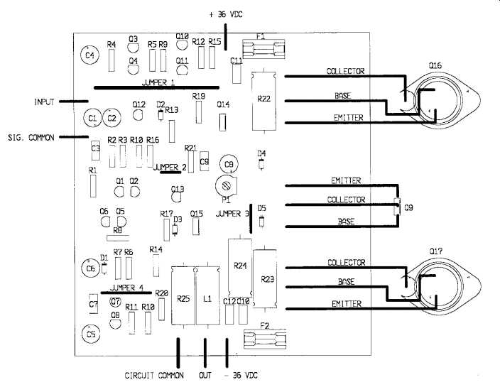
FIG. 12 Top-view silkscreen of the 50-watt professional-quality amplifier.
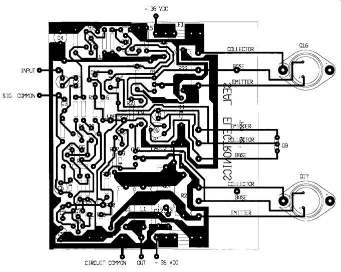
FIG. 13 Top-view silkscreen of the 50-watt amplifier showing top view
of the PC board artwork.
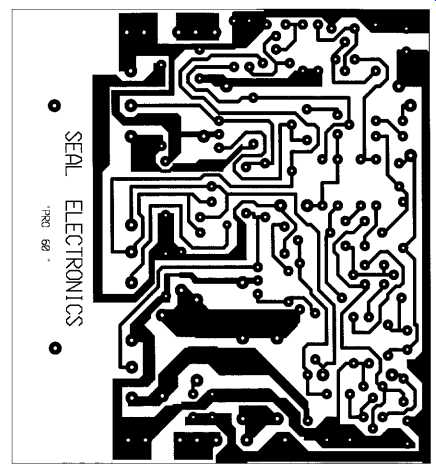
FIG. 14 Bottom-view reflected artwork for the 50 watt professional quality
amplifier.
Constructing the Professional-Quality Audio Power Amplifier
If you would like to construct the professional-quality audio power amplifier as described above, I have provided a professional layout design (Figs. 12 and 13) and the PC board artwork (FIG. 14) for you to copy.
See Section C for a full-size copy of FIG. 14, to be used in your project. I have constructed amplifiers more involved than this using the PC board "fabrication by hand" process described earlier, so it is not overly difficult to accomplish if you have a little time and patience. Also, I have constructed similar amplifiers on perfboard, but this process is really time-consuming, and you are more prone to make mistakes. Naturally, the preferred method of construction is to fabricate the PC board as illustrated using the photographic technique. Regardless of the method you choose, the amplifier circuit is reasonably forgiving of wire or trace size, and component placement. If you would like to avoid the task of PC board fabrication all together, a complete kit (including etched and drilled PC board) is available from SEAL Electronics (the contact information is provided in Section B).
The parts list for the professional-quality amplifier is provided in Table 2. Most of these components are available at almost any electronics supply store, but a few details need to be highlighted. If you want to go first class on this project, you can use 1% metal film resistors for all of the 1/2-watt resistors listed. Metal film resistors will provide a little better signal-to-noise performance, but it is probable that you will not be able to hear the difference-standard 5% carbon film resistors will provide excellent performance. Output inductor L1 is easily fabricated by winding about 18 turns of either 16 or 18 AWG "magnet wire" around a 1/2-inch form of some type (I use an old plastic ink pen that happens to be 1/2 inch in diameter). The exact inductance of L1 is not critical, so don't become unduly concerned with getting it perfect.
TABLE 2 Parts List for 50-Watt Professional-Quality Audio Amplifier
All of the transistors used in this amp are readily available from MCM Electronics or Parts Express (contact information is provided in Section B of this textbook), as well as many other electronic component suppliers.
The fuse clips used in the PC board design are GMA types (four needed) with two solder pins that insert through the holes in the PC board. Pay particular attention to the orientation of transistors Q14 and Q15 when soldering them into the PC board-it is easy to install them backward.
You should mount a small TO-220-type heatsink to Q14 and Q15. Almost any type of TO-220 heatsink will be adequate, since the power dissipation of Q14 and Q15 is very low. A common style of heatsink that will be ideal is U-shaped, measuring about ¾ x 1 inch (w x h) (width x height), constructed from a single piece of thin, stamped aluminum.
You will need one medium-sized heatsink for the output transistors (i.e., Q16 and Q17) and the Vbias transistor (Q9). Just to provide you with a rough idea of the size of this heatsink, the commercial models of this amplifier use a heatsink that measures 6 x 4 x 1 1/4 (l x w x d) (length x width x depth) (if you're lucky enough to find a heatsink accompanied with the manufacturer's thermal resistance rating, the specified rating is 0.7°C/watt). However, if this is all confusing to you, don't worry about it.
If you can find a heatsink that is close to the same dimensions and is designed for the mounting of two TO-3 devices, it should suffice very well. A few examples of larger heatsink styles are provided in FIG. 15; the square-shaped Wakefield type in the forefront of the illustration is a good choice for this amplifier project. If the heatsink is manufactured so that it can be mounted vertically, there is space provided for mounting it directly to the PC board. If not, you can run longer connection wires out to an externally mounted heatsink (the length of the transistor connection wiring in this design is not critical). Q9 should be mounted in close proximity to the output transistors on the same heatsink so that it will thermally track the temperature of the output transistors. The connection wiring to Q16, Q17, and Q9 can be made with ordinary 20- to 22-AWG stranded, insulated hookup wire. Be sure to double-check the accuracy of your wiring according to the silkscreen diagrams provided-it's very easy to get the transistor leads confused on the TO-3 devices.
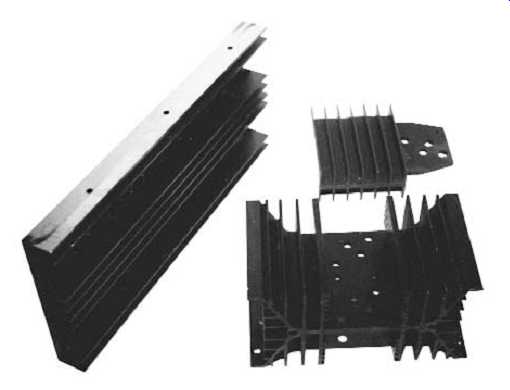
FIG. 15 Some examples of larger heatsink styles.
Testing, Setup, and Applications of the Professional-Quality Audio Power Amplifier
Once you have finished the construction of the amplifier, I suggest that you use the schematic (FIG. 11) and accompanying illustrations (Figs. 12 to 14) to recheck and then double-recheck your work. The amplifier design of FIG. 11, like all modern high-quality audio power amplifier designs, is classified as direct-coupled. This term simply means that all of the components in the signal path are directly coupled to each other, without utilizing transformers or capacitors to couple the signal from one stage to the next. Direct-coupled amplifiers provide superior performance, but because of the direct-coupled nature of the interconnecting stages, an error in one circuit can cause component damage in another (a damaged electronic circuit causing subsequent damage in another electronic circuit is referred to as collateral damage). Therefore, it is extremely important to make sure that your construction is correct; one minor mistake is all that it takes to destroy a significant number of components.
The amplifier of FIG. 11 is designed to operate from a "raw" dual polarity power supply providing 42-volt rail potentials. Under these conditions, it is very conservatively rated at 60 watts rms of output power into typical 8-ohm speaker loads. The design also performs very well with dual-polarity rail voltages as low as 30 volts, but will provide proportionally lower output power. FIG. 16 illustrates a good power supply design for this amplifier. As shown, it will provide dual-polarity rail potentials of about 38 volts. This equates to a maximum power output of a little over 50 watts rms.
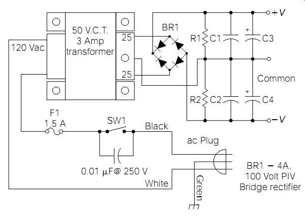
FIG. 16 Recommended power supply for 50 watt audio amplifier.
There are a few details that bear mentioning in the power supply design of FIG. 16. The 0.01-uF capacitor connected across the power switch (SW1) is provided to eliminate "pops" from the amplifier when the switch is opened. Note that when SW1 is open, the full 120-volt AC line voltage will be dropped across the 0.01-uF capacitor, so the capacitor should be rated for about 250 volts (the peak voltage of ordinary 120-volt AC residential power is about 170 volts). R1 and R2 are called bleeder resistors, and they are incorporated for safety reasons. Referring back to the amplifier schematic of FIG. 11, imagine that a failure had occurred causing the rail fuses (F1 and F2) to blow. With the rail fuses blown, the filter capacitors of the power supply (i.e., C3 and C4 in FIG. 16) do not have a discharge path. Therefore, they could maintain dangerous electrical charges for weeks, or even months. If you attempted to service the amplifier without recognizing that the filter capacitors were charged, you could suffer physical injury from accidental discharges. R1 and R2 provide a safe discharge path for the filter capacitors to prevent such servicing accidents.
R1 and R2 can be 5.6-Kohm, 1/2-watt resistors for this power supply. C1 and C2 are typically 0.1-uF ceramic disk capacitors providing an extra measure of high-frequency noise filtering on the power supply lines. They are seldom required, and may be omitted if desired. The capacitance value for the filter capacitors (i.e., C3 and C4) should be about 5000 _F (or higher), with a voltage rating of at least 50 WVDC.
While on the subject of power supply designs, the power supply illustrated in Fig. 6 (sec. 6) will also function very well with this amplifier design.
You may want to consider this approach if you have difficulty finding a 50-volt center-tapped, 3-amp transformer (if you decide to use the Fig. 5-6 circuit for the amplifier power supply, it would be a good idea to install bleeder resistors as illustrated in the FIG. 16 design).
After connecting the FIG. 11 audio power amplifier to a suitable dual-polarity power supply, adjust P1 to the middle of its adjustment range and apply operational power. If either one of the rail fuses blows (i.e., F1 or F2), turn off the power immediately and correct the problem before attempting to reapply power. If everything looks good, and there are no obvious signs of malfunction, use a DVM to measure the DC voltage at the amplifier's speaker output (i.e., the right side of L1). If the amplifier is functioning properly, this output offset voltage should be very low, with typical values ranging between 10 and 20 mV.
If the output offset voltage looks good, measure the DC voltage from the emitter of Q16 to the emitter of Q17, and adjust P1 for a stable DC voltage of 47 mV. Once this procedure is accomplished, the amplifier is tested, adjusted, and ready for use.
From a performance perspective, the input sensitivity of this power amplifier design is approximately 0.9 volts rms. The rms power output is a little above 50 watts using the power supply design of FIG. 16. The signal-to-noise ratio (SNR) should be at or better than _90 dB, and the total harmonic distortion (% THD) should be better than 0.01%. The amplifier can drive either 8- or 4-ohm speaker load impedances. Its design is well suited for domestic hi-fi applications, and since it includes excellent short-circuit and overload protection, it is also well suited for a variety of professional applications, such as small public address systems, musical instrument amplifiers, and commercial sound systems.
Speaker Protection Circuit
I decided to include this project as a final entry in this section, because it is a good example of how various circuit building blocks can be put together to create a practical and functional design, and also because it represents the last electronic "block" in an audio chain starting from the preamplifier and ending at the speaker system.
There are several problems associated with high-performance direct-coupled amplifier designs, such as the design illustrated in Fig. 11. If one of the output transistors (Q16 or Q17) failed in the amplifier of FIG. 11, it is probable that one of the DC power supply rails could be shorted directly to the speaker load (bipolar transistors normally fail by developing a short between the collector and emitter).
DC currents are very destructive to typical speaker systems, so it is very possible that a failure in an audio power amplifier could also destroy the speaker system that it is driving. Another problem relating to audio power amplifiers is their power-up settling time (often called turn-on transients). When operational power is first applied to most higher-power audio amplifiers, they will exhibit a temporary period (possibly as long as 100 milliseconds) of radical output behavior while the various DC quiescent voltages and currents are "settling" (balancing out to typical levels). This settling action usually produces a loud "thump" from the speakers during power-up, which is appropriately referred to as "turn-on thumps."
FIG. 17 Speaker protection circuit.
FIG. 17 illustrates a very useful, practical, and easy-to-construct circuit that can be implemented into almost any audio system to eliminate the two aforementioned problems associated with direct-coupled audio power amplifiers; (1) it automatically disconnects the speaker system from the audio power amplifier if any significant level of DC current is detected at the amplifier's output; (2) it delays connection of the amplifier to the speaker for about 2 seconds on power-up, thereby eliminating any turn-on thumps; and (3) it provides a visual "status" indication of the amplifier's operation utilizing a typical LED indicator.
Operational power for the FIG. 17 protection circuit is normally obtained from the secondary of the power transformer used in the power supply for the audio power amplifier (the current drain of this circuit is very low, so it shouldn't represent any significant load to any large power transformer used to provide high currents to an audio power amplifier). The connection terminal extending from the negative side of C3 should be connected to the center-tap of the power trans former-the transformer center-tap will always be the circuit common point (see FIG. 16). The connection point extending from the anode of D1, labeled "ac in" in FIG. 17, is connected to either "hot" side of the transformer secondary (e.g., either 25-volt secondary wire coming out of the 50-volt center-tapped transformer of FIG. 16).
Referring to FIG. 17, D1 and C3 make up a simple half-wave rectifier circuit, providing a rectified and filtered DC voltage from the AC operational power obtained from the secondary of the power transformer.
For example, if you connected this circuit to the 50-volt transformer secondary of FIG. 16 (as described previously), the DC voltage at the cathode of D1 should be approximately 35 volts (25 volts _ 1.414 _ 35.35 volts DC). ZD1 and R1 form a simple zener voltage regulator circuit. Typically, R1 is a 220-ohm, 1-watt resistor and ZD1 is a 24-volt, 1-watt zener diode.
D3, R2, R3, C6, Q4, Q5, D9, and the relay form a time-delay relay circuit. When AC power is first applied to the AC input (i.e., the anode of D1), D3 is forward-biased only during the positive half-cycles. The positive pulses are applied to the RC circuit of R2 and C6. Because of the RC time constant, it takes several seconds for C6 to charge to a sufficiently high potential to turn on the Darlington pair (Q4 and Q5) and energize the relay. D9 is used to protect the circuit against inductive kickback spikes when the relay coil is deenergized. R3 is incorporated to "bleed" off C6's charge when the circuit power is turned off.
Transistors O2 and Q3 and their associated circuitry form the familiar astable multivibrator (discussed in previous sections of this textbook).
The values of C4 and C5 (typically 1 _f) are chosen to cause the circuit to oscillate at about 2 hertz.
The protection circuit of FIG. 17 is designed to accommodate "two" audio power amplifiers, since most domestic hi-fi applications are in stereo. The outputs of the audio power amplifiers are connected to the "right in" and "left in" connection points, while the right and left speaker systems are connected to the "right out" and "left out" connection points, respectively. If you desire to provide protection to only one speaker system (obviously indicating that you will be using only one audio power amplifier), you can delete F2 and R5, and the output relay need only be a single-pole, double-throw (SPDT) type. Fuses F1 and F2 are speaker fuses.
Their current ratings will depend on the power capabilities of your audio power amplifier and speaker system.
Since the operational power for this protection circuit is obtained from the power transformer in the audio power amplifier's power supply, operational power to this circuit will be applied simultaneously to applying power to the amplifier(s). Therefore, when the operational power is first turned on, the speakers will not be connected to the power amplifier(s) because the relay will not be energized. The relay will not energize until C6 reaches a potential high enough to turn on Q4 and Q5. This will take several seconds. In the meantime, the audio power amplifier(s) will have had sufficient time to stabilize, thereby eliminating any turn-on thumps from being applied to the speaker systems.
While C6 is charging, before Q4 and Q5 have been turned on, the astable multivibrator is oscillating, causing LED1 to flash at about 2 hertz. This gives a visible indication that the protection circuit is working, and has not yet connected the speakers to the power amplifier(s).
When the time delay has ended and Q4 and Q5 turn on, the collector of Q4 pulls the collector of Q3 low, through D8, stopping the oscillation of the multivibrator, and causing LED1 to light continuously. The relay energizes simultaneously. By staying bright continuously, LED1 now gives a visual indication that the circuit is working, and that the speakers are connected to the power amplifier(s). At this point, the protection circuit of FIG. 17 has no further effect within the amplification system unless a DC voltage occurs on one or both of the audio power amplifier outputs.
Under normal conditions, when no DC voltage is present on the output of either of the audio power amplifiers, the amplified audio AC signal from both power amplifiers is applied simultaneously to R4, R5, C1, and C2. Because the time constant of the RC circuit is relatively long, C1 and C2 cannot charge to either polarity. In effect, they charge to the aver age value of the AC waveshape, which is (hopefully) zero. This is the same principle as trying to measure an AC voltage level with your DVM (digital voltmeter) set to measure DC volts-pure AC will provide a zero reading.
If a significant DC voltage (i.e., higher than about 1.2 volts) appears on the output of either power amplifier, C1 and C2 will charge to that voltage regardless of the polarity (note that C1 and C2 are connected with both positive ends tied together, forming a nonpolarized electrolytic capacitor-this principle was discussed when describing the FIG. 11 amplifier circuit). This DC voltage will be applied to the bridge rectifier (D4 through D7). Although it might seem strange to apply DC to a bridge rectifier, its effect in this circuit is to convert the applied DC to the correct polarity for forward-biasing Q1 (a technique often called steering). When Q1 is forward-biased, it pulls the base of the Darlington pair (Q4 and Q5) low, deenergizing the relay, and disconnecting the speaker systems from the power amplifiers before any damage can result. At the same time, the astable multivibrator is enabled once more, causing LED1 to flash, which gives a visual indication that a malfunction has occurred. The circuit will remain in this condition as long as any significant DC level appears on either of the power amplifier outputs. On removal of the DC, the protection circuit will automatically resume normal operation.
Transistors Q1 through Q5 can be almost any general-purpose NPN types; common 2N3904 transistors work very well. The contact ratings of the relay must be chosen according to the maximum output power of the audio power amplifier(s). The voltage ratings for all of the electrolytic capacitors should be 50 WVDC for most applications. However, if the operational AC power obtained from the power amplifier's power sup- ply transformer is higher than 30 volts AC, you will have to adjust most of the component values in the circuit to accommodate the higher operational voltages. The diode bridge consisting of D4 through D7 can be constructed from almost any type of general-purpose discrete diodes (e.g., 1N4148 or 1N4001 diodes), or you can use a small "modular" diode bridge instead.