by J.L. Linsley Hood
M.I.E.E. Robins Electronics
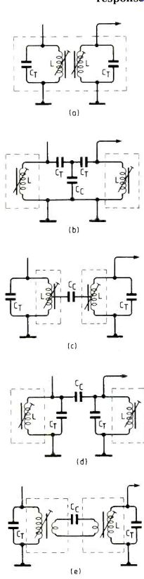
Fig.1. IF transformer at (a) used in valve receivers. Alternatives shown
(b) to (e) also provide band-pass response.
This unusual design attempts to match the much sought after sound quality of the postwar five-valve radio designs.
It is perhaps a rather offhand commercial attitude to a.m. radio, rather than simple nostalgia or an affection for things using valves that has resulted in the relatively high prices paid for late pre-war or immediately post-war 'table' radio sets.
The reason for this is that these sets were built at a time when a.m. radio reception was the only kind there was, and considerable efforts were made by their manufacturers to achieve the highest practicable quality in the final output signal, and this is normally vastly better than that given by their contemporary equivalents.
There is, therefore, a temptation to the circuit designer to look at the possibilities in this field, and to see how to use some of the good electronic components now available, to put together a contemporary receiver design which would be at least as good as its valve-operated forerunners, without being excessively elaborate or expensive in its construction.
The circuit construction employed for these classic radio sets was invariably of the superhet form. This technique, as it was then employed, allowed the necessary selectivity to be obtained without undue curtailment of the wanted a.f. sidebands by the use of at least two pairs of bandpass-coupled tuned circuits.
These were typically of the form shown in Fig.1(a) where the required inter-circuit coupling is obtained by positioning the coils side by side within the common screening can, so that there is the required degree of mutual inductance.
In the average modern transistor radio, the a.m. i.f. transformers are most commonly of the single-tuned circuit type, which does not give a very good compromise between selectivity and bandwidth, and this appears to be true regardless of whether these circuits are built from discrete transistors, or, more typically nowadays, with some single i.c. that combines the function of local oscillator, frequency changer, i.f. amplifier and demodulator on a single chip.
The fields in which improvement should therefore be sought are in the band-pass characteristics of the i.f. stages to give an optimum compromise between selectivity and bandwidth, in sensitivity, in the distortion introduced by the demodulator stage and in the quality of the subsequent audio amplification.
I.f. transformer design
Starting with the first of these, an immediate problem is that the majority of the small commercial i.f. transformers, designed for use with transistor radios, are of single-coil construction. Those of the type shown in Fig.1(a), though available, are not often used, and are therefore expensive and not very easy to come by.
Fortunately, there are a number of alternative methods of achieving a band-pass characteristic, of which I have shown the more practicable structures in Figs 1(b)-1(e). Most of the common i.f. coils have taps on their windings, or small secondary coils, to match the desired high dynamic impedance of the tuned circuit to the input impedance of the junction transistor, which would allow the use of the forms shown in Fig.1(c) or (e), and because the size of the coupling capacitor (Ce) required for this layout (in the range 100-1000pF) is a lot larger than the likely stray capacitances, and the signal voltages are relatively low, these forms would lend themselves well to circuits in which the coupling capacitor value was altered, by switching, to give a choice of selectivities.
The layout of Fig.1(b) would be particularly well suited to a switched-selectivity i.f. amplifier, since the value of C,, for critical coupling could be of the order of a hundred times greater than that of the tuning capacitors (Ce), (Cc= 0.1µF if Ct is 1000pF), and the r.f. voltage developed across Ce would be proportionately low, since one end would be returned to the chassis line.
For a fixed-selectivity i.f. amplifier, the layout shown in Fig.1(d) is probably the simplest answer, since it works equally well with a wide range of coils, whether or not these have tapped primaries or secondary windings.
The variety of amplitude response curves which are given by coupled tuned transformers of this type is shown in Fig. 2, in which Fig. 2(a) shows the transmission/frequency characteristics of an under-coupled pair of tuned circuits (similar to that which would be given by two such tuned circuits in cascade), and 2(e) shows the effect of over-coupling two such tuned circuits. In practice, the coupling factor, k, would be chosen to give a response curve close to that shown in (c) called ‘critical coupling', though some excursions on either side of this value could allow bandwidth alteration without too great a degree of departure from the desired flat-topped curve.
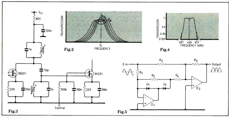
--- Fig. 2-5 Response curves provided by tuned circuits at Fig. 1 depending
on degree of coupling, Fig.2. I.f. stage using circuit at Fig.1(d), with
a.g.c. applied to fet amplifier rather than to frequency changer, Fig.3,
and its response, Fig. 4.Opamp demodulator, Fig. 5.
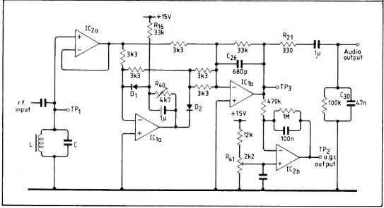
Fig. 6. Practical circuit based on demodulator of Fig. 5.
A comprehensive analysis of the design of band-pass coupled i.f. transformers is given by Sandel, and a summary of the design data for the type of circuit shown in Fig.1(d) is that for critical coupling the coupling factor (k) should be the reciprocal of the mean Q value for the two coils. If these have a Q of 100, a fairly typical value, then the coupling capacitor (Ce) should be Ct.k, where k=0.01. If the tuning capacitors, (Ci), are 1000pF, then the coupling capacitor value should be 10pF. Having tested a number of miniature i.f. coils, the great majority intended for use as a single tuned circuit were found to tune over the range 450- 470kHz with a 1000pF capacitor, and under these conditions, had a working Q value of about 100. These coils would therefore be very suitable for this particular application.
Those with an internal tuning capacitor, usually housed in larger cans, are normally of higher quality, and have a higher L/C ratio, which leads to the use of a smaller value capacitor and also to a higher working Q value. The circuit layouts of Fig.1(c), or 1(e), would be more appropriate in these cases. Unless the secondary coil or tap ratio can be determined, it is impracticable to calculate the required value of Ce, but this may easily be determined by experiment and will usually lie in the range 100-800pF. Too high a Q value for the i.f. transformer tuned circuits is not very desirable where a series of these are to be operated in cascade; the effect of this is multiplicative in the steepness of attenuation of the skirt of the pass band. For example, with three such band-pass pairs, as might be used in a high quality receiver design, a Q value for each coil of 100 will give a pass band of about 12kHz at-6dB, and 20kHz at -60dB. A Q of 200 at each stage would reduce the useful pass-band from 12 to 6kHz. For this reason I was quite happy to discover that the inexpensive miniature i.f. coils were in the required Q range.
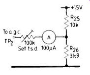
Fig.7. Signal-strength meter uses a.g.c. voltage from TP2.
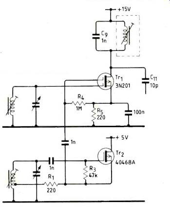
Fig.8. Oscillator and frequency changer stage.
Fig.9. Circuit diagram of receiver for long and medium waves. Additional coils and switching can be used to obtain h.f. coverage, but second-channel interference will be inevitable, though no more than in valve-operated receivers.
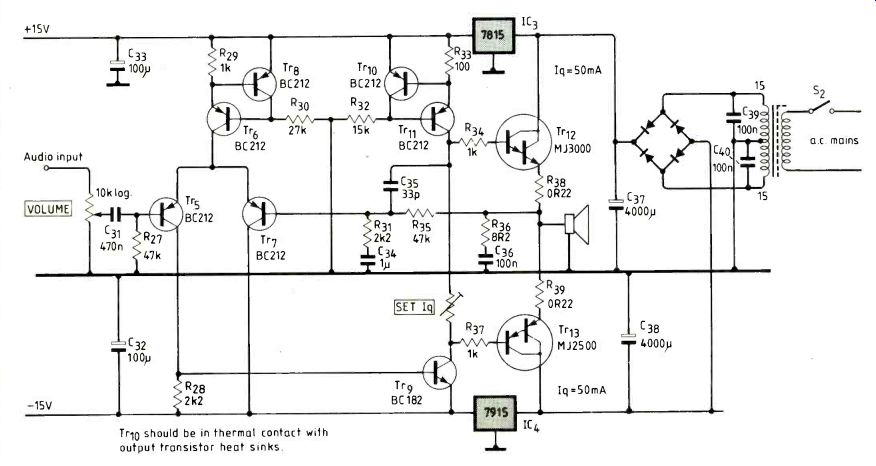
Fig.10. Audio output amplifier and power supply.
Sensitivity
To give the type of performance needed to match the old-style `table' radio set, an aerial sensitivity of at least 10µV is needed, for 6dB s/n ratio. Two i.f. gain stages using dual-gate mosfets will easily attain this value at the input to the i.f., assuming a `detector' (demodulator) signal level of 100mV, and two such i.f. stages will allow an adequate range of gain control by means of a signal-derived a.g.c. voltage, without the need to apply such a control voltage to the frequency changer, which might cause oscillator frequency drift. I have shown a suitable i.f. stage layout in Fig.3. When the coils are correctly aligned, the pass-band is as shown in Fig.4.
Demodulator distortion
The normal diode envelope detector used in the average a.m. receiver does not have a very good performance, with introduced harmonic distortion levels lying anywhere in the range 0.5 to 20%.
However, there is a useful op-amp configuration in which the gain of the op-amp is used to remove the diode dead-band and provide a precision full-wave a.c. rectifier, Fig.5.
Its method of operation is as follows. For the positive-going half of an input cycle, the output of IC1 will drive the cathode of D2 negative, until the potential at the junction of D2 and R2 is equal, and opposite to that applied to the input. In this mode, IC1 acts as a unity-gain inverting amplifier, and a negative-going current input is applied to the ‘virtual earth' point at the inverting input of IC2.
For a negative-going half cycle applied to the rectifier input, the output of IC1 will be positive, which will drive D1 into conduction, and D2 will be open-circuit. As the inverting input of ICI also forms a 'virtual earth', there is no potential across R2 and R4, and the current input to IC2 is simply that which flows from the source through R3.
On both halves of the input cycle, therefore, a negative-going current input is applied to the inverting input of IC2, which causes an equal, but opposite current to flow from IC2 output, through R5, to preserve the necessary voltage node at the inverting input.
Resistor R4 must have a value equal to half that of R3 so that there will be the required negative-going total current flow to IC2, on the positive-going input half cycle, when current is flowing through both R4 and R3.
I have shown a practical form of this circuit in Fig.6, in which two dual op-amps provide a low distortion demodulator and a.g.c. amplifier.
In this, IC2a is a unity-gain impedance converting buffer stage to provide the desired low impedance drive to the precision rectifier without loading the secondary coil of the final i.f. band-pass circuit, and a small forward bias is applied to the diodes D1 and D2, by means of R16 and R40i to assist the circuit to operate in a nearly ideal manner.
It is easy to set this up. With no input to IC2a, (TP1 shorted to the OV line), the output of ICtb should also be zero. As R40 is gradually increased in value, current is fed through DI, which causes the output of ICta to move negatively until D2 just begins to conduct.
When this happens, the output of ICtb starts to go positive, as measured at TP3. The correct setting for R40 is at the threshold of this output voltage excursion.
Since one is only interested in the 1.f. component of the output, the capacitor C26 reduces the h.f. gain of ICib, to leave only the modulation voltage. It is prudent to ensure that this part of the circuit is well screened from the aerial input, or otherwise there will be a spurious signal at twice the if., 930kHz, which is within the medium waveband.
Components R21 and C30 also help to remove the 930kHz component from the audio output line.
In practice, the incoming i.f. signal generates a mean positive potential at the output of ICob that is proportional to the signal strength. This is amplified and inverted by IC2b to give an a.g.c. potential which becomes progressively more negative as the signal strength increases. Variable R41 sets the a.g.c. potential, in the absence of an incoming signal (TP1 shorted to the 0V line), to +4V which is a suitable value for the second gate of the dual-gate mosfets. TP2 can also be used as a source of potential to operate a signal strength or tuning meter, as shown in Fig.7.
This provides an effective and fast-acting a.g.c. system, which holds the audio output substantially constant over a range of input signal strengths from 5uV - 5mV. The inevitable penalty for such a sensitive receiver is that there is a considerable increase in aerial and other noise when the set is tuned between signals.
Oscillator and frequency changer
This is a conventional circuit layout, as shown in Fig. 8, in which a single-gate depletion mosfet is used as a source-coupled oscillator, with the drive to the frequency changer being taken from the low impedance source electrode. The inclusion of R1 converts the drive waveform into a rounded square wave, of about 800mV pk-pk amplitude, which gives good conversion efficiency in the frequency changer.
Although r.f. mosfets are somewhat dearer than bipolar junction transistors, their use in the oscillator, frequency changer and i.f. stages is amply justified by the performance advantages which they confer: high mutual conductance, high input impedance, and a relatively high output impedance, which lessens the extent of damping of the tuned circuits and removes the need for tapped coils.
Also, in the i.f. stages, the very low feedback capacitance of the dual-gate mosfet avoids problems of r.f. instability. In the frequency changer stage, the mosfet offers a second input electrode, unconnected to the signal gate, for local oscillator injection, and as an oscillator, the mosfet offers a superior performance in terms of output and frequency stability to any other transistor type.
Incidentally, if a single gate mosfet is not available, a dual-gate device, such as the 3N201, can be used with the two gates joined together.
The complete receiver
I have shown the circuit of the complete a.m. receiver in Fig. 9, which includes provision for switching between the l.w. and m.w. bands, (150-300kHz and 550-1600kHz).
Audio stage
I decided on a target performance of 3 watts into a 3 ohm load-a typical 'table radio' output power figure-at not more than 0.05% t.h.d. with good reactive load behavior, and with all crossover products being substantially less than 0.01%. The circuit I eventually chose for the audio amplifier, which fully met this specification, is shown in Fig.10, as is also that used for the power supplies.
The final performance of the unit has proved very satisfactory, both in respect of its ability to recover very weak signals at good entertainment quality--completely unseen by my domestic 'trannies'--and in respect of its frequency stability and tonal characteristics.
[*Sandel. B., Radio Designers Handbook, R. Lanford-Smith (Ed.), 4th Edition, (2), Chapter 26. Iliffe Ltd. ]
----------------------
Also see:
Developments in packaging (Dec. 1986)
Mains communication without tears
==========
(adapted from: Wireless World , Dec. 1986)