Custom i.c’s reduce oscilloscope manufacturing time and costs but also improve reliability.
by Johan Helfferich and Eppi Kruisdijk
[ The authors are with Philips' Enschede facility in The Netherlands.]
One of the principal design objectives in Philips' medium-frequency oscilloscopes was a significantly reduced component count. Primarily to reduce manufacturing time and cost-thereby permitting a low selling price-this would also ensure high reliability and simplify service and troubleshooting.
To achieve this aim, a number of custom i.cs were specially developed with the expectation that large production volumes for these new instruments would allow the relatively high costs of developing custom i.c’s to be recovered.
A number of the i.c’s used are of particular interest and they are the preamplifier, channel switch, display logic/control circuit, peak-to-peak detector and auto level circuit and the integrated time-base logic circuit. These are all custom i.c’s.
The preamplifier consists of a unity-gain amplifier, a x 10 gain amplifier, a two-quadrant multiplier, a multiplier control circuit and power supply and switching circuits.
Only one of the two amplifiers is active at any time. This separation of the x 1 and x 10 amplifier sections provides a pulse response which is independent of the setting.
Signal delay is also almost constant for the different settings. Input sensitivities are 20mV/div. for the x 1 amplifier, and 2mV/div. for the x 10 amplifier and output is a symmetrical current of 100µA/div.
To provide variable amplification, a two-quadrant multiplier is built in. The multiplier is a new development with eight transistors featuring stable multiplication and a pulse response independent of the multiplication factor over the entire range.
To translate control voltage from the variable potentiometer into a stable multiplication, the preamplifier has a special multiplier control circuit which limits the variable range from 1:1 to 1:2.5. A switching circuit with Ltd.--compatible input activates the x 1 or X10 amplifier.
Switching of the vertical channels and trigger selection in the PM3055 is done by the integrated channel switch, Fig. 1.
This i.c. consists of two current switches to switch channels on and off, two inverters for inversion of channel B if required and two circuits for positioning or leveling the signals (dual timebase). The inverters are used as slope switches in the trigger path.
The display logic and control circuit was developed to control all the vertical channel switches, trigger selectors and timebase selector, Fig. 2.
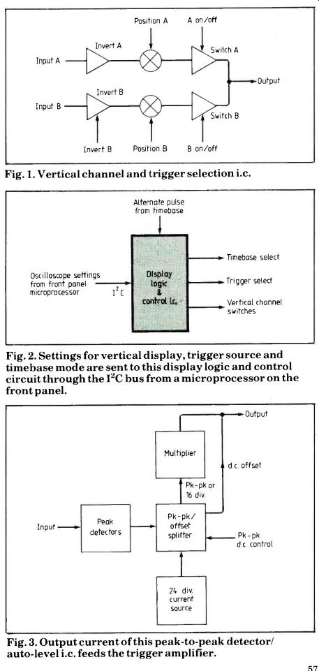
Fig. 1. Vertical channel and trigger selection i.c.
Fig. 2. Settings for vertical display, trigger source and timebase mode are sent to this display logic and control circuit through the I2C bus from a microprocessor on the front panel.
Fig. 3. Output current of this peak-to-peak detector / auto-level i.c. feeds the trigger amplifier.
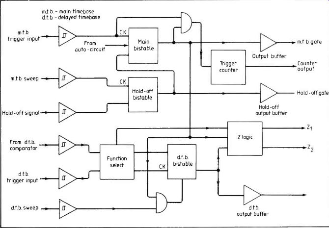
Fig. 4. Implementation of the auto-set function shows both sections of
the integrated timebase logic i.c.
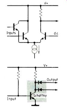
Fig. 5. Both current-mode logic, top, and integrated Schottky logic, bottom, are used for the timebase logic i.c. of Fig. 5.
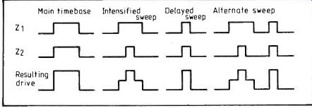
Fig. 6. Tube drive waveforms with intensified and delayed sweeps.

Fig. 7. Main and delayed time-base triggering.
Settings of the vertical display, trigger source and time-base mode are transmitted to the display/control circuit via the I2C bus from the microprocessor in the front panel. After setting, the control circuit autonomously sends the correct signals to the channel switches, trigger switches and time base selector in a number of modes including alternate, chop, composite triggering, alternate time base etc.
In the 3055, the display / control i.c. makes it possible to display from one to eight traces. The i.c. controls A, B, add and trigger-view traces which can be displayed in main, main-intensified, delayed or alternate-time-base modes. This circuit operates in two modes-peak-to-peak leveling and d.c. leveling.
In d.c. model the 16-div. current is separated from 24-div. current. The 16-div. part feeds the multiplier. Controlling the multiplier with the level potentiometer gives a level variable through 16 signal divisions.
Residual current is fed directly as a common-mode signal to the output pins.
In the peak-to-peak mode, a part of the signal proportional to the signal's pk-to-pk value is fed to the multiplier, controlled by the level potentiometer.
Residual current is modulated with the mean d.c. value of the signal's two peak values and fed to the output pins. Output current peak-to-peak detector/auto-level i.c., Fig. 3, is fed to the trigger amplifier.
Using this principle in peak-to-peak mode gives d.c. rejection on both trigger and trigger-view signals independently of the waveform and signal duty cycle. In this mode, only the level potentiometer influences the position of the trigger view over signal amplitude.
Figure 4 shows the integrated timebase logic i.c. All main and delayed time-base logic for the new medium-frequency oscilloscope family is incorporated in one full-custom chip.
This chip starts and stops the main and delayed time-bases and opens and closes the seven output gates. It also cooperates with the vertical display-selection i.c. in alternating time-base mode.
Communication with the setting processor takes place through a serial bus and reaches the chip through a series-to-parallel converter.
Also implemented in this time-base logic is the circuit that counts triggers on the trigger input during the main time-base sweep. This circuit makes the auto-set function possible (Fig. 4) which always endeavors to include at least three periods of the input signal on screen.
The chip has two sections containing the fast circuit and the other handling slower function-selection operations.
The first section is implemented in current-mode logic and the second in integrated Schottky logic, well known from its use in gate arrays, Fig. 5. Design of the fast section posed the greatest problems as it proved to be difficult to simulate analogue circuits running at twice the bandwidth of the oscilloscope.
To ensure that none of the transistors saturates, the input Schmitt trigger and the bistable circuit that starts and stops the sweep are analogue.
Delay between the trigger inputs and the start sweep output is kept as small as possible, which makes the necessary delay line as short as possible.
Function selection inputs are TTL-compatible.
Intensity signals Z1 and Z2 make it possible to drive the c.r.t. with intensified and delayed sweeps, Fig. 6. The delayed time-base comparator is not incorporated on the chip.
Figure 7 shows triggering of main and delayed time-bases.
----------------------
Also see:
Link |
Link | --Mains communication without tears
Electronic ignition for single-cylinder engines
==========
(adapted from: Wireless World , Dec. 1986)