by Alan Clements, Ph.D, Teesside Polytechnic
The three parts of this article are based on part of a book 'The 68000: software, hardware and interfacing' to be published next spring by PWS Boston, who are represented in the UK by Wadsworth International.
----
MEX68KECB, referred to in September's article, is Motorola's 68000 educational computer board, requiring power supply and v.d.u. terminal. The ECB has powerful monitor called Tutor which enables 68000 programs to be entered, debugged and executed. Although now somewhat dated its monitor is the basis of most educational and training systems on the market.
-----------
Large memory arrays can be produced economically with dynamic ram provided care is taken over timing requirements, refreshing and the supply rail. Part 3 concludes the series.
The simplified circuit diagram of the dynamic refresh generator on the 68000 board is given in Fig. 20, and its timing diagram in Fig. 21. A refresh clock operating at 7.54kHz signals the need for a burst of refresh cycles every 1/(7.54 x 103) = 0.133 ms. This design does not carry out all refreshes in one burst-it performs eight cycles every 0.133ms, completing all 128 row refreshes in 0.133 x 16 = 2.128ms. By distributing the refresh operation over 16 bursts of eight cycles, the processor is not held up for any appreciable length of time.
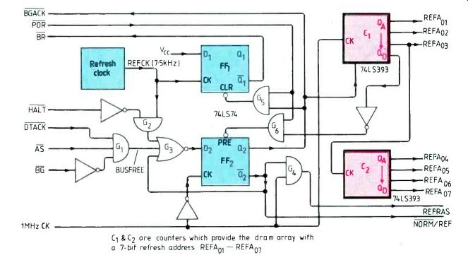
Fig. 20. Dynamic refresh generator on the 68000 educational board distributes
refresh operation over 16 bursts of eight cycles so that the processor
is not held up appreciably. Timing diagram is at Fig.2, over.
The refresh control circuitry on the board uses the 68000 bus arbitration signals, ßR (bus request, Bc (bus grant) and BGACK (bus grant acknowledge). When 1. is asserted by a device wishing to control the system bus, the 68000 responds by asserting its BG output. The requesting device recognizes Bc and then waits until the end of the current bus cycle before asserting BGACK to claim ownership of the bus.
Once BGACK has been asserted, the requester may release BR and the old master releases B i.
The new master owns the bus until it releases BGACK. A power-up, POR (power-on-reset from the processor control circuitry) goes low, clearing FF1 setting FF2. Any well-designed circuit should be similarly initialized and placed in a "safe state". In this state, Q 1 (i.e. BO is negated and Q2 (i.e. NORM/RE) is low, signifying normal operation. When the refresh clock, a simple RC oscillator, generates a rising edge, FF1 is set and BR asserted. The 68000 detects the bus request and asserts bus grant sG and-gate G1 detects the condition Bc = 0, As = 1 DTACK = 1, which occurs when the 68000 has relinquished the bus and forces input D2 of FF2 low. Note that the other two inputs to nor-gate G3 (at this time) are both low-one because we will assume HALT is negated and the other because Q2 (NORM/ RRF) is low after FF2 has been preset.
When D2 is low, FF2 is cleared on the falling edge of the 1MHz clock. Output Q2 is connected to the 68000 bus BGACK input and, while low, stops the processor from regaining control of the bus. At the same time, it forces the output of and-gate, G5 low, clearing FF1 and negating 13R. Thus FF1 has done its job in this burst of refresh cycles and is once more in its initial state.
When FF2 is cleared, its Q2 output goes high; it is also the NORM/REF line controlling the address multiplexer to the ram array. When high, NORM/REF selects the address from the refresh column-counter (i.c’s C1 and C2). The output Q2 is also fed back to the D2 input of FF2 via or-gate G3, so that once Q2 is high the flip-flop is held in this state and no longer depends on the state of Bc from the processor, as BG is automatically cleared following the negation of BR. Flop-flop 2 is now "locked up", Q2 high, and can only be released by the assertion of its PRE (preset) input.

Fig. 21. Timing diagram for Fig.20.

Fig.22. Structure of TMS4500A dynamic
ram controller which produces additional MUX, CAS and RAS signals,
and generates refresh control and arbiration signals required by the d-ram.
The final role played by Q2 is to gate the 1MHz clock in and-gate G4, the output of which is the pulsed Rñs needed in the refresh cycle. Because Q2, when low, allows counter C1 to operate, three bits of the refresh address appear on REFA01 to REFA02 Which form part of the dynamic ram's row refresh address. This counter is clocked at the refresh rate-1MHz.
A second-state counter, C2, is clocked by C 1 after eight cycles and provides the remaining four row refresh addresses-REFA03 to REFA07.
After the three-bit counter C1 has produced eight pulses, its Qd output rises and disables and-gate G5. This presets FF2, causing Q2 (i.e. BGACK) to be negated, freeing the processor by releasing BGACK and Q2 (i.e. NORM/REF) to go low, disabling and-gate G4 and removing the refresh clock (REFRAS). The system is now in its normal state, with BR, BG and BGACK all negated. The only change since the start of the cycle is that counter C2 has been advanced by one, so that the next time the refresh clock generates a pulse, the following eight row addresses will be refreshed.
TMS4500A dynamic ram controller
I have always been surprised that the semiconductor manufacturers have done so little to make it easy to interface drams to microprocessors.
Some d-ram controller chips have appeared, but most of' them perform little more than address multiplexing and the generation of a refresh address. The designer still has to generate the RAS, CAT and multiplexer timing signals. To be fair, it is not easy to design a d-ram controller because the timing requirements of d-ram chips are very stringent if they are to be operated at their limits.
Several controllers have been designed which include all timing and control functions on one chip and which can make a d-ram array look almost like a static ram array.
One such device is the Texas Instruments TMS4500A. I am going to briefly overview the chip, but I do not intend to wade through the data sheet and applications manual in any detail here. Figure 22 illustrates its structure. A 16-bit address from the microprocessor is applied to RA0-RA7 and CAo-CA7 and is latched into the controller by the address latch enable input, ALE. If the cs input is active-low when it is latched by ALE, a memory access begins.
The 4500 places the row address on its MAo-MA7 outputs and awaits a negative-going edge at its ACR or its ACW input. These inputs (one for a read cycle and one for a write cycle) are used to multiplexer the column address onto MA0-MA7 and to assert the CAS output. All timing is performed by a clock input to the 4500. Three of the inputs, TWST, FS0 and Fs1 are used to program the clock frequency, the number of wait states per access (zero or one) and the length of the refresh cycle.
Although a refresh can be forced at any time by strobing the REFREQ pin, it is Convenient to operate the 4500 in a hidden refresh mode. the 4500 performs a single refresh automatically at a rate determined by the clock input and its programming pins. If the controller is accessed by the processor when a refresh is due, either the processor or the controller must wait. An internal arbitration mechanism determines which goes first.
The recommended interface between a 4500 and a 68000 microprocessor is show in Fig. 23. The address on A01-A16 from the 68000 is latched into the 4500 by ñs. The ADR input is clocked by a delayed version of the ñs pulse, providing a suitable Ws to CAS delay.
Note that Acw is permanently connected to Vice. Two banks of d-ram are provided; one strobed by LDs and one by 1.1)s. A clever feature of this circuit is that the DTACK acknowledge to the 68000 is derived from CAS from the 4500 controller. If ever the 4500 is carrying out a refresh cycle when the 68000 requests a memory access, CAS remains high until the refresh has been completed and the 68000 is held up until the access can take place.
There are two approaches to the design of memory systems using controllers such as the TMS4500A. One is to assume that the circuit of Fig. 23 will work because it is from the manufacturer's application notes. The other is to take the data sheets of the 68000, the 4500 and the d-ram chip and to put them all together to determine whether any parameters are violated.
Problems in dynamic memory design Although this article has concentrated on timing diagrams, that is not the whole of the store. Dynamic ram is associated with at least two other nasty problems! the current taken is very "bursty" and the current taken by the V,,. pin can rise at a rate of 50mA/ns when the RAs input is asserted.
This corresponds to a rate of change of 50 million amps per second. Such a rate of change can cause the V,. voltage at the terminal of the chip to fall to a point at which erratic operation may occur. The power supply problem is solved by a combination of attention to the circuit layout and to decoupling. The power lines to each ram chip are made as wide as possible to reduce their impedance and a 0.1µF capacitor is connected between ground and V at each chip-or at least at every other chip. This capacitor provides the current surge required by the chip whenever RAs goes low.
Another peculiarity of the dynamic ram follows from the way in which it generates an internal back-bias supply. The back-bias does not stabilize for at least 200µs after the initial application of V. Therefore, d-ram should not be accessed until at least 2001.1s after the system has been powered up.

Fig. 23. The TMS4500A dynamic ram controller allows the 68000 processor
to be connected to d-ram in almost the same way as static ram.
----------------------
Also see:
Link | --Mains communication without tears
==========
(adapted from: Wireless World , Dec. 1986)