AMAZON multi-meters discounts AMAZON oscilloscope discounts
Section 3 showed that although a passive filter is easy to build, it has two serious disadvantages. One is that V_out is necessarily less than V_in . The loss in signal strength is considerable in a high-order filter consisting of many stages. The second disadvantage is illustrated in Figure 13, in which it is seen that the response curve is broadly rounded in the region around the cut-off frequency. This means that it is not possible to retain a signal of a given frequency while making a useful reduction in a signal of a closely neighboring frequency.
While increasing the order of the filter makes the cut-off curve steeper for frequencies much higher than the cut-off point it has very little effect in the region of cut-off itself. In other words, we need to give the curve a sharper 'knee'.
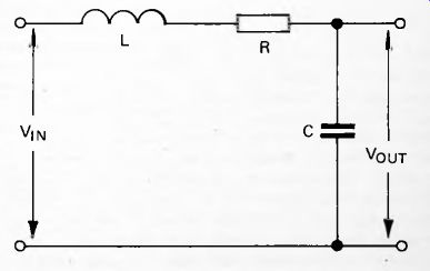
Fig. 23. Second-order LC filter.
One way of improving the shape of the curve is to include an inductor in the filter. Figure 23 shows one type of second-order LC low-pass filter. This has two components which are reactive, the inductor and the capacitor. At low frequencies the inductor has low reactance, passing the signal readily to the low-pass filter consisting of R and C. The capacitor has high reactance at low frequencies so the signal passes on with little or no reduction in strength. At high frequencies the inductor has high reactance, reducing signal strength which is further reduced by the RC combination, owing to the low reactance of the capacitor. The overall effect is a low-frequency pass-band and a -12dB per octave fall in the cut-off region.
A more important effect is what happens around the -3dB point. At that point the reactance of the inductor equals that of the capacitor. As can be seen in Figure 8, for an RC filter at the frequency at which R = Xc, the waveform of Vc, the alternating voltage across the capacitor lags behind the V_R waveform by 90°. In a filter consisting of an inductor and a resistor, at the frequency at which R = XL, the con
verse applies. The voltage VL across the inductor leads VR by 90°. If the filter has an inductor, a resistor and a capacitor, as in Figure 23, and the frequency is such that R = Xc = XL, the same applies; Vc lags V_R by 90° and VL leads V_R by 90°. Consequently, the phase angle between Vc and VL is 180°. They are exactly out of phase.

Figure 24--The result of Vc and VL being out of phase is a state of maximum
oscillation in the filter. We say that it resonates.
The idea of resonance is best illustrated by thinking of a bare room, such as a bathroom, in which there are few soft furnishings. A little experimentation in such a room reveals that there are one or more frequencies at which, if you sing gently, the room 'booms' loudly, accentuating these particular frequencies. Resonance in a room can be a serious matter, particularly in a concert hall. It is also a problem which concerns designers of loudspeaker cabinets. Resonance is a state at which the input of energy is in phase with the natural oscillations of the system. An example of this is the transfer of energy when you rhythmically push a child on a swing.
Provided that you deliver each forward push at exactly the right moment, when the child is moving forward, a little extra energy is transferred to the child at each oscillation. The amplitude gradually builds up. If you deliver the pushes at the wrong frequency, you are eventually pushing the child forward when the swing is moving backward, and the amplitude decreases.
In an LRC filter at its -3dB frequency, the input signal is delivering energy to the filter at its natural rate of oscillation.
Consequently voltage swings increase in amplitude. As Vc increases, VL decreases, and vice versa. Thus the swing of V_c is not opposed but rather is enhanced by the swings in VL. Thus V_c , which is also the output voltage of the filter, has its maximum amplitude. The result is shown in Figure 24, in which there is a peak of output around the resonant frequency.
This peak 'sharpens' the knee of the curve around the cut-off frequency. Given certain combinations of R, Xc and XL the peak may be even higher, so that the filter shows overall gain around the cut-off frequency.
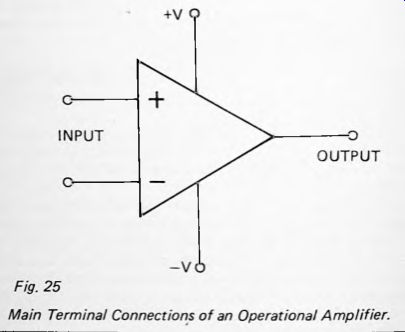
Figure 25
An inductor improves the performance of a low-pass filter and the same applies to high-pass and other types of filter.
Several inductors may be used in filters of higher orders. But there are disadvantages in using inductors so, if possible, we prefer to replace them with operational amplifiers.
Before we describe how this is done, we need to examine the main features of this type of amplifier.
Operational Amplifiers
Operational amplifiers, or op amps as we shall call them from now on, were built originally from discrete components.
Nowadays they are almost without exception realized as integrated circuits. Many types of op amp are available as two or four identical amplifiers in a single I.C. package.
Figure 25 shows the main terminals of an op amp. There are two inputs, which we refer to as the non-inverting (+) input and the inverting (-) input. Both of these inputs have a very high impedance. That is to say, very little current flows into or out of these terminals. In a typical op amp the input impedance is 2M ohm and in some types of op amp the input impedance may be as high as 10^12 ohm, or 1 tera-ohm, so that the current flowing can be totally ignored. The difference between the two inputs is described later.
There is a single output terminal which, in contrast with the input terminals, has very low impedance, typically 75 ohm. It can supply a relatively large output current without a significant drop in the output voltage.
Finally, there are the two power supply terminals. Usually an op amp is operated on a dual power supply. The ground rail is taken as the reference voltage, 0V. The power rails have voltages equally above and below the ground rail. For example, if the power supply is ±6V, the +V terminal is at +6V and the -V terminal is at -6V.
Op amps often have two additional terminals for balancing the circuit, particularly for correcting for errors in the amplifier which make it behave as if there is a small difference between the input voltages when in fact there is not. In the applications described in this guide, such errors are too small to be important so we are not concerned with how to correct them.
Returning to the input terminals, we see from Figure 25 that they have opposite polarity. The relationship between input and output is as follows, assuming that voltages more positive than +V or more negative than -V are not allowed:
Input conditions
Both inputs at the same voltage
(+) input at higher voltage than (-)
(+) input at lower voltage than (-)
•Output voltage always referenced to the 0-V line.
Resulting output
Zero volts
Positive
Negative
The size of the output voltage, whether positive or negative, depends on the difference between the voltages at the two inputs, so the op amp is a differential amplifier. Further it has very high gain (200,000 or more) so that a very small difference in voltage is often sufficient to make the output swing as far as it can toward +V or -V. This gain is referred to as the open loop gain. Note that there is an upper limit to the rate at which the output of an op amp can change. This is known as the slew rate. This varies from one type of op amp to another. If the slew rate is low, the output is not able to respond fully to rapidly alternating input signals. As a result the effective gain of the amplifier falls off at higher frequencies. In most amplifiers the output voltage can swing to within a volt or so of the supply rails, but no further. In a few types the output can swing almost to +V and -V. No amplifiers are able to produce an output beyond the range +V to -V.
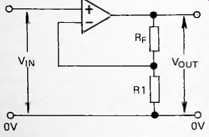
Fig. 26. An op amp wired on a non-inverting amplifier, (power connections
not shown).
With the features described above, the op amp is a versatile device that can be used in a variety of ways. Here we consider only two ways in which it is commonly used in filter circuits. The first of these is the non-inverting amplifier. This is an amplifier in which the output is greater than the input and has the same polarity. Figure 26 shows that the circuit involves feedback. Furthermore, since the feedback goes to the (-) input terminal, it is negative feedback. This type of feedback limits the gain and causes the circuit to have overall stability of operation.
In Figure 26 the feedback resistor RF and resistor R1 act as a potential divider. If the potential at the junction of R f and R1 is v then:
R1 v ~ PoUT x
*f + R1
The voltage v is fed back to the (-) input. If V_IN increases a very little above v, so that the difference between V_IN and v is just enough to produce the output V_out the circuit reaches a stable state in which:
Pout--Ax (Pin--v) where A is the open loop gain of the amplifier.
This gives:
V_out
= Kin-v.
A
But A is very large compared with V_out so that the expression on the left of the equation approximates to zero and thus:
-v = 0 or v = V_in
In words, the circuit becomes stable when the voltages at the input terminals are almost equal. They are not exactly equal as this would make V_out become zero. The small difference between them (amplified by 200,000 times or more) is just enough to give the required output voltage.
Substituting V_in for v in the first equation we find:
R1 V in – V out x Rf + R1
or
*f + R1
V_out – V in x R1
The gain of the amplifier circuit (as opposed to the huge open loop gain of the op amp IC) is thus (RF + R1)/R1.
For example, if and Rf = 100 k, the gain is (100k + 10k)/10k = 11 . Note that the gain of the circuit is determined only by the vales of the resistors, not by the performance of the opamp IC. If high-precision resistors are used the gain is set with great precision.

Fig. 27. Unity-gain amplifier (power connections not shown).

Fig. 28.
An op amp wired as an inverting amplifier (power connections not shown).

Fig. 29. Flow of current in an inverting amplifier circuit.
One special case of the non-inverting amplifier is illustrated in Figure 27. In this the whole output voltage is fed back to the (-) input. Thus v = V_out and the circuit becomes stable when Vout = V_in. The gain is 1. This circuit is sometimes known as a voltage follower. Although the circuit produces no gain, it has the property that it requires only a very small input current, yet can supply a relatively large output current.
This is a very useful property for matching impedances, that is to say, for providing ample current where it is needed.
The other important circuit configuration for an op amp is the inverting amplifier (Fig. 28). This too has negative feedback and so, as before, V_out is such that the input voltages are almost equal. In this circuit the (+) input is held at 0V, so (-) will be very close to 0 V too. Figure 29 explains what happens. Given a positive input voltage V_IN a current I flows toward the (-) terminal which is at 0 V. Ohm's Law tells us that I = V_in/R1. This current does not enter the input terminal, which has very high impedance, but carries on through the feedback resistor and enters the output terminal.
An equal current I flows through the feedback resistor and so the value of V_out must be such as to cause that current to flow:
I= -Vout/Rf. The minus sign indicates that here I is flowing away from the (-) terminal. Since it is the same I in both resistors we find:
--------
The gain of this circuit is -RF/R1. The negative sign shows If Rf = 100k, for that this is an inverting amplifier, example, and R1 = 10k, then the gain is -100k/100k = -10.
One point about this circuit is that the voltage at the (-) terminal is always very close to 0V. In effect the (-) terminal is at 'ground' or 'earth' potential and is often known as a virtual earth.
We now see how the various types of amplifier circuit described above are made use of in active filters.
Simple Low-pass Filter
Figure 30 shows the circuit of what is known as a 1st order low-pass section. It is called '1st order' because it has only one stage of filtering. This implies that there can be other stages of filtering to follow it. It could be just a 'section' of a much more elaborate filter circuit.
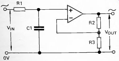
Fig. 30 -- 1st order low-pass section.
Comparing Figure 30 with Figures 12(b) and 26, it is clear that this is simply an ordinary RC passive filter followed by a non-inverting amplifier. R1 and C1 determine the cut-off frequency, while R2 and R3 set the amount of amplification.
As far as filtering goes, it inherently has the same properties as the RC passive filter. The improvements are:
(1) The output from the RC stage is amplified to restore or enhance the output voltage.
(2) The low output impedance of the amplifier means that a larger current can be drawn from the output without over-loading the filter section and degrading its performance.
VCVS Filters
The name of these filters is derived from the fact that we use the op amp as a voltage-controlled voltage source.

Fig. 31. 2nd order low-pass section.
The first stages of the circuit of Figure 31 are similar to the second-order low-pass filter of Figure 16, except that C1 is connected to the output of the amplifier instead of being grounded. The important point is that although the amplifier has negative feedback to its (-) input, as in Figure 26, the feedback to the first filter stage is positive. As explained on page 40, negative feedback tends to make a circuit stable.
By contrast, positive feedback such as we have here, makes a circuit unstable. It tends to make it oscillate.
We sometimes experience the effect of positive feedback with a public address system, when the volume is turned up too high and the amplified sound from the loudspeakers is readily picked up by the microphone. The sound reaching the microphone is amplified again and the process goes on and on with increasing volume. The effect is strongest at certain frequencies so that what begins as a small noise ends as a very loud screeching sound. The system is resonating at that frequency.
Now to return to the filter of Figure 31. At low frequencies the capacitors have little effect, since they block the trans
mission of the signal to ground or to the output side of the amplifier. The signal passes to the amplifier and is amplified or not, depending on the ratio between R3 and R4. At high frequencies C1 passes the signal to the output side, but it is reduced because it passes to the potential divider R3/R4, and then to the (-) input. This causes the output to swing in the opposite direction to the signal and nullifies its effect.
Thus at both low and high frequencies the circuit behaves very much as a 2nd order passive low-pass filter, except for the amplification and the increased output impedance that we had in the filter of Figure 30.
Given the conclusions of the previous paragraph it might be wondered what is so special about such a filter. The clue comes when we examine the behavior of the circuit for an incoming signal that is close to the cut-off frequency. At this frequency the positive feedback action comes into play.
The circuit resonates. The amplitude of the output is enhanced for signals at and around that frequency. The graph of V_out/V_in shows an upward bulge around the cut-off frequency. In fact it has a shape very much like the response of an LC filter (Fig. 24). The crucial part of the response curve, the 'knee', has been sharpened without resorting to inductors.
The extent to which the filter resonates near the cut-off frequency can be controlled by varying the ratio between the two capacitors. If C1 is large compared with C2, resonance is strong and the response curve peaks sharply. We say that the filter is under-damped (Fig. 32). At the other extreme, if C1 is small compared with C2, there is little resonance and the filter is highly damped. In fact its frequency response may be little different from that of a passive filter. By a careful choice of capacitor values the resonance can be controlled so that exactly the right amount of damping occurs. The filter is critically damped.
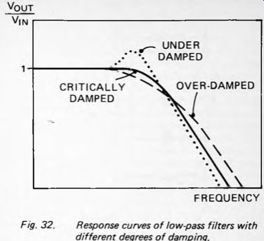
Figure 32
One particular version of the VCVS filter is the Sallen and Key filter. In the Sallen and Key filter the gain of the amplifier is 1. In other words the amplifier is wired as a unity gain amplifier (Fig. 27). The circuit is the same as Figure 31 except that R3 and R4 are omitted and there is negative feedback directly to the (-) input.

Figure 33
Orders of Active Filters
So far we have described the 1st order and 2nd order sections which have a roll-off in their cut-off regions of -6dB and -12dB per octave. The 2nd order filter introduces the possibility of controlled damping. As with passive filters, we can cascade such sections together to obtain increasing rates of roll-off. A 3rd order filter, for example, is made by connecting the output of a 1st order section to the input of a 2nd order section.
The roll-off of this filter is--18dB per octave. In general we make multiple filters of even orders (2nd, 4th, 6th, etc.) by cascading one or more 2nd order sections.
Multiple filters of odd orders (1st, 3rd, 5th, etc.) are made by beginning with a 1st order section and cascading after it as many 2nd order sections as are required. As an example, Figure 33 shows a 5th order low-pass filter made from a 1st order section followed by two 2nd order sections.
Types of Response
The performance of a multi-section filter depends upon the responses of the sections of which it is composed and, since the output of one section becomes the input of the next, the response of any given section depends partly upon the characteristics of the sections preceding and following it. In designing a multi-section filter the relationships between the sections have to be carefully calculated with reference to the filter as a whole. This means that very often the cut-off frequency will be different for each section, as will the amount of damping. The mathematics involved is complex but, as a result of this, we are able to produce filters with various combinations of desirable characteristics.
The features that define the characteristics of a filter are:
(1) Cut-off frequency
(2) Roll-off
(3) Damping
(4) Flatness of the pass-band
(5) Overshoot
(6) Time delay
We have already dealt with the first three features but must briefly discuss the others. The pass-band of a passive filter is almost perfectly flat; V_out is equal to V_in until the cut-off frequency is approached (Fig. 13). This is not necessarily the case with multi-section active filters. Interactions and resonances may cause certain frequencies in the pass-band to pass slightly more strongly than others. Thus the ratio of V_OUT may lead to ripples in the pass band (Fig. 34), the more sections in the filter the more ripples.
Overshoot is the tendency of the output to swing too far when there is a sudden change of input level. It then oscillates for a short while before settling at its final correct level (Fig. 35). Obviously, this is an undesirable characteristic, as it introduces distortion into the output.
When a signal passes through a filter it is subject to a change of phase, or time delay. The amount of delay varies to V_in within the pass band varies with frequency. This with frequency. As shown, it is clear from Figure 2 that most signals consist of a mixture of a number of waveforms at different frequencies. Filtering imposes a different amount of delay on each component of the signal. The signal emerging from the filter has the same components but their relative timing is different. The effect may be quite small but the result is that the signal is distorted, a factor that may be crucial in certain applications. The effect is more pronounced at lower frequencies.
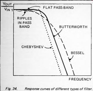
Fig. 34

Fig. 35. Overshoot.
Well beyond the cut-off region, in the stop band, the slope of the response curve is -6dB, -12dB or more per octave depending only on the order of the filter. It is only necessary to know how steep the curve is intended to be and produce a filter of the required order. It is mainly in the pass-band and the transition region around the cut-off point that design becomes critical. The designing of filters is nearly always a matter of compromise. For example, the factors that operate in the direction of keeping the pass-band flat also operate to reduce the slope of the curve just beyond the cut off point. Unfortunately, all that the designer can do is to specify the relative cut-off frequencies and the amount of damping of each section of the filter, and calculate what the resulting response of the filter will be.
There would seem to be an infinite range of possibilities, but most filters fall in one or the other of three main groups:
1. Butterworth filter. The pass band is very flat (Fig. 34), and overshoot is not excessive, but the slope in the transition region is poor. It also has poor phase characteristics. This type of filter is often recommended as the best for general use, owing to its theoretically flat pass-band. However, in practical versions of this filter the effects of tolerance in component values is to introduce ripples in the pass-band and it usually loses its main advantage.
2. Chebyshev filter. This has a steep slope in the transition region at the expense of ripples in the pass-band. Phase response is poor, so that distortion due to this is greater than in the other filters. There are a number of designs of Chebyshev filter, classified according to the depth of the ripples in the pass-band, usually 1, 2 or 3dB.
3. Bessel This has the least phase effect, since phase change is less dependent on frequency in this filter. Distortion of the waveform in the pass-band is at a minimum. On the other hand it is the worst filter with regard to steepness of slope in the transition region.
These are the filters that are made simply by cascading together the 1st-order and 2nd-order sections already described. There are other ways of building low-pass active filters, several of which are examined in the sections which follow.
PROJECT 2--Simple Intercom Level 2
This is a basic intercom circuit but has the special feature of a filter to improve the quality of the sound. Cost is reduced in this project, as in most inexpensive intercoms, by using the loudspeaker to double as the microphone. For the sake of compactness, the loudspeakers used in intercoms are usually of small diameter, and as a result, high frequencies are emphasized and sound tends to be 'tinny'. In this project we use an active low-pass filter to remove the high-frequency components of the signal. The intercom has many uses in the home or office. Since only one station is transmitting at any one time, it is very suitable as a 'baby-listener'.
How It Works
The master station unit contains the main circuit (Fig. 36), the control switch (S1) and the twin 6V batteries which provide the power supply. The slave station consists only of a loudspeaker. Thus it is possible for the master station to call the slave station, but not vice versa. This may be considered a disadvantage by some users but, to others, one-sided control is a definite advantage. This arrangement has the advantage of minimizing the number of components required. A bell or buzzer system can be installed to give two-way calling facilities if this is really essential.
The circuit is based on a single IC which contains four JFET operational amplifiers. We use three of these, the first ( IC1a) as a pre-amplifier to condition the signal ready for filtering. The second amplifier ( IC1b) is used for the filter, and the third ( IC1c) as an output amplifier. In the description, we assume that S1 is switched to position 2, so that the master station is transmitting and the slave station is receiving.
When the user speaks into the loudspeaker LS1, the motion of the loudspeaker coil in the field of the loudspeaker magnet induces an alternating e.m.f. in the coil. This e.m.f. is passed across C1 to the first amplifier which is wired as an inverting amplifier (Fig. 28) with gain variable from 1 to 100. The output from this goes to a 2-pole active low-pass filter, which has a roll-off in the stop band of -12dB per octave. The values of the resistors and capacitors are chosen so as to give a Butterworth response (page 51) with cut-off frequency at about 900Hz. If a slightly crisper tone is preferred, 27nF or 47nF capacitors can be substituted for C2 and C3. Although the filter has a certain amount of gain, we need additional gain to produce a sound audible above a modest background of noise. IC1c, wired as an inverting amplifier with fixed gain of 27 provides this.

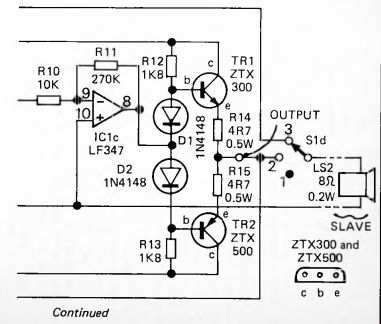
Fig. 36
The output stage consists of a conventional Class AB push-pull circuit. This consists of two emitter-follower circuits connected back to back. There is no voltage amplification at this stage, but the emitter-followers are capable of providing sufficient power to drive the loudspeaker of the slave station LS2. Only low-wattage (0.2W) speakers are used so the output transistors are rated for 500mA. No heat sink is necessary for the transistors. The function of the diodes is to bias the base of each transistor so that it begins to conduct immediately the voltage from IC1c departs from zero. For example, because of the voltage drop across the junction of D1, the base of TR1 is always 0.6V above the output of IC1c. Thus as soon as the output begins to exceed 0V, the base of TR1 is brought above 0.6V and the transistor begins to conduct. If it were not for these diodes, neither transistor would conduct until the output of the amplifier was more than +0.6V or less than -0.6V. Small signals (less than ±0.6V) would not be heard at all! Also, there would be a serious distortion of the waveform every time it crossed the zero level.
The rest of the circuit is concerned with controlling the direction of transmission. S1 is a 4-pole 3-way rotary switch.
In position 1 both the power lines from the batteries are disconnected and the intercom is off. In position 2, LS1 is connected to the input side of the amplifier system and LS2 is connected to the output. The master talks to the slave. In position 3 the reverse applies, and the slave can talk to the master.
Construction
The main point about construction is to lay out the components as compactly as possible to reduce the pick-up of mains hum. Since the op amps are all contained in a single IC, a rectangle of strip-board 100mm x 74.1mm (one of the standard sizes) is more than adequate. Only low-cost loudspeakers are required; it is sometimes possible to buy a matching pair--each already mounted in boxes. With luck, there will be room in one box for the circuit-board and batteries. Unless conversations are unduly prolonged, current requirements are small.
Depending on the volume setting, the project requires about 15mA on each power line. Thus it is feasible to operate it from a pair of PP1 6V batteries, or from four AA or AAA cells in a battery holder. It also operates on ±9V so a pair of PP3 9V batteries can be used, with an appreciable increase in the volume of the sound.
The connection between the master and slave is made with a pair of light-duty wires. For convenience, fit a jack plug and socket where the cables enter the enclosures.
If this is turned too high, there will be distortion and the circuit may break into oscillation. Further increase in volume, if required, can be obtained by increasing the value of R11. Alternatively, remove R14 and R15 and replace the transistors, using medium-power transistors such as a BD131 (npn) for TR1 and a BD132 (pnp) for TR2. These will require clip-on or bolt-on heat sinks.
In use, the volume is set by adjusting VR1.
Special Components
Semiconductors:
D1, D2 1N4148 silicon signal diodes (2 off)
ZTX300 npn transistor ZTX500 pnp transistor
TR1
TR2
Integrated Circuit
IC1 LF347 (or TLr074) quad JFET op amp
Miscellaneous:
LS1,LS2 8-ohm 0.2W miniature loudspeaker, approx. 50mm diameter recommended, though any 'spare' 8-ohm speaker could be used, or even 4-ohm or 15-ohm (2 off) 4-pole 3-way rotary switch, with knob.
S1